

Sony CXD2467Q Datasheet
Digital Signal Driver/Timing Generator
Description
The CXD2467Q incorporates digital signal processor
type RGB driver and timing generator functions onto a
single IC. Operation is possible with a system clock up
to 135MHz (max.). This IC can process video signals
in bands up to SXGA standard, and can output the
timing signals for driving various LCD panels such as
SXGA (LCX028) and XGA (LCX017 and LCX023).
Features
• Various picture quality adjustment functions such
as user adjustment, white balance adjustment and
gamma correction
• OSD MIX, black frame processing, mute and limiter
functions
• Drives various data projector LCD panels such as
SXGA (LCX028) and XGA (LCX017 and LCX023)
• Controls the sample-and-hold position of the
CXA2112R sample-and-hold driver
• Line inversion and field inversion signal generation
• Supports AC drive of LCD panels during no signal
Applications
LCD projectors and other video equipment
Structure
Silicon gate CMOS IC
Absolute Maximum Ratings (VSS = 0V)
• Supply voltage VDD VSS – 0.5 to +4.0 V
• Input voltage VI Vss – 0.5 to VDD + 0.5 V
• Output voltage VO Vss – 0.5 to VDD + 0.5 V
• Storage temperature
Tstg –55 to +125 °C
Recommended Operating Conditions
• Supply voltage VDD 3.0 to 3.6 V
• Operating temperature
Topr –20 to +75 °C
– 1 –
E98X38-PS
Sony reserves the right to change products and specifications without prior notice. This information does not convey any license by
any implication or otherwise under any patents or other right. Application circuits shown, if any, are typical examples illustrating the
operation of the devices. Sony cannot assume responsibility for any problems arising out of the use of these circuits.
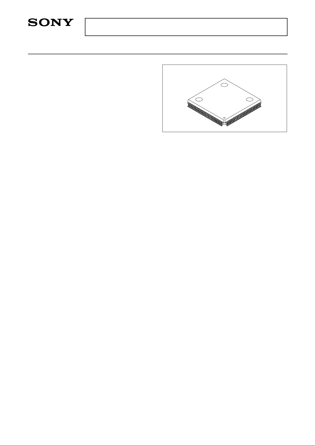
CXD2467Q
240 pin QFP (Plastic)
Note) Company names and product names, etc. contained in these materials are the trademarks or registered
trademarks of the respective companies.
For the availability of this product, please contact the sales office.
– 2 –
CXD2467Q
Block Diagram
PARALLEL I/F
DSD
TG
IRACT
8 × 2 × 3
R, G, B IN
R, G, B OUT
CLKOUT
HRET, ORACT, HST,
HCK1, HCK2, DCK1,
DCK1X, DCK2,
DCK2X, ENB, PCG,
CLP1, CLP2, VST,
VCK, FRP, BLK,
RGT, XRGT, DWN,
HB, VB1, VB2, SHA,
SHB, SHC, SHD, INV
XCLRDirect Clear
IRRET, IRACT
PSAVE1
PSAVE2
10 × 2 × 3
2 × 2 × 3
R, G, B OSD
2
YM
2
YS
PCTL
PCLK
PDAT
CLK2
CLK1P
CLK1N
CLK1C
10
CLKSEL1
CLKPOL1
CLKSEL2
HDIN1
HDPOL1
VDIN1
VDPOL1
CLK4
HDIN2
HDPOL2
CLK3P
CLK3N
CLK3C
CLKSEL3
CLKPOL2
CLKSEL4
D
Q
Q
D
Q
Q
– 3 –
CXD2467Q
Pin Configuration
1 2 3 4 5 6 7 8 9 10 11 12 13 14 15 16 17 18 19 20 21 22 23 24 25 26 27 28 29 30 31 32 33 34 35 36 37 38 39 40
72
73
74
75
76
77
78
79
80
81
82
83
84
85
86
87
88
89
90
91
92
93
94
95
96
97
98
99
141142143144145146147148149150151152153154155156157158159160161162163164165166167168169170171172173174175176177178179180
190
191
192
193
194
195
196
183
182
181
184
185
186
187
188
189
197
198
199
200
201
202
203
204
205
206
207
208
209
210
211
212
213
214
215
216
217
218
219
220
221
222
223
224
225
226
227
228
229
G2OSD0
B2OSD1
B2OSD0
YM2
YS2
VDD
VSS
PCTL
PCLK
PDAT9
PDAT8
PDAT7
PDAT6
PDAT5
PDAT4
PDAT3
PDAT2
V
DD
VSS
PDAT1
PDAT0
HDIN1
VDIN1
HDPOL1
VDPOL1
CLK1P
CLK1N
VSS
CLK1C
VSS
CLK2
VSS
41 42 43 44 45 46 47 48 49 50 51 52
CLK3N
VDD
VSS
CLK3C
VSS
CLK4
CLKSEL3
CLKSEL4
CLKPOL2
IRRET
HRET
V
SS
53 54 55 56 57 58 59
XCLR
VDD
VSS
B2OUT0
B2OUT1
B2OUT2
B2OUT3
60
B2OUT4
CLKOUT
VSS
CLKSEL1
CLKSEL2
CLKPOL1
HDIN2
HDPOL2
CLK3P
R1IN1
R1IN2
R1IN3
R1IN4
R1IN5
V
SS
VDD
R1IN6
R1IN7
PSAVE2
PSAVE1
TEST4
TEST3
TEST2
TEST1
ORACT
IRACT
V
SS
VDD
INV
SHD
SHC
SHB
SHA
CLP2
CLP1
PRG
FRP
XRGT
RGT
VSSHST
DCK2X
DCK2
DCK1X
DCK1
V
DD
HCK2
HCK1
BLK
135136137138139140
ENB
VSSVDD
VCK
VST
DWN
134HB133
VSS
132
VB1
131
VB2
130
PCG
129
R1OUT9
VSS
B1OUT4
B1OUT5
B1OUT6
B1OUT7
B1OUT8
V
SS
B1OUT9
G2OUT0
G2OUT1
G2OUT2
61
62
63
64
65
66
67
68
69
70
71
B2OUT5
B2OUT6
B2OUT7
B2OUT8
B2OUT9
V
DD
VSS
B1OUT0
B1OUT1
B1OUT2
B1OUT3
V
SS
G2OUT3
G2OUT4
G2OUT5
G2OUT6
G2OUT7
V
DD
VSS
G2OUT8
G2OUT9
G1OUT0
G1OUT1
G1OUT2
V
SS
G1OUT3
G1OUT4
G1OUT5
G1OUT6
G1OUT7
V
SS
G1OUT8
G1OUT9
R2OUT0
R2OUT1
R2OUT2
V
SS
R2OUT3
R2OUT4
R2OUT5
R2OUT6
R2OUT7
V
DD
VSS
R2OUT8
R2OUT9
R1OUT0
R1OUT1
R1OUT2
R1OSD0
R1OSD1
B2IN0
B2IN1
B2IN2
B2IN3
B2IN4
V
SS
B2IN5
B2IN6
B2IN7
B1IN0
B1IN1
B1IN2
B1IN3
B1IN4
B1IN5
B1IN6
B1IN7
V
SS
VDD
G2IN0
G2IN1
G2IN2
G2IN3
G2IN4
G2IN5
G2IN6
G2IN7
G1IN0
G1IN1
V
SS
G1IN2
G1IN3
G1IN4
G1IN5
G1IN6
G1IN7
R2IN0
R2IN1
R2IN2
R2IN3
V
SS
VDD
R2IN4
R2IN5
R2IN6
R2IN7
R1IN0
111
110
109
108
107
106
105
118
119
120
117
116
115
114
113
112
104
103
102
101
100
230
231
232
233
234
235
236
237
YS1
YM1
V
SS
VDD
B1OSD0
B1OSD1
G1OSD0
G1OSD1
238
239
240
G2OSD1
R2OSD0
R2OSD1
127128
R1OUT8
V
SS
126
VDD
125
R1OUT7
124
R1OUT6
123
R1OUT5
122
R1OUT4
121
R1OUT3
– 4 –
CXD2467Q
Pin Description
Pin
No.
Symbol I/O Description
Input pin
processing
for open status
1
2
3
4
5
6
7
8
9
10
11
12
13
14
15
16
17
18
19
20
21
22
23
24
25
26
27
28
29
30
31
32
G2OSD0
B2OSD1
B2OSD0
YM2
YS2
VDD
VSS
PCTL
PCLK
PDAT9
PDAT8
PDAT7
PDAT6
PDAT5
PDAT4
PDAT3
PDAT2
VDD
VSS
PDAT1
PDAT0
HDIN1
VDIN1
HDPOL1
VDPOL1
CLK1P
CLK1N
VSS
CLK1C
VSS
CLK2
VSS
I
I
I
I
I
—
—
I
I
I
I
I
I
I
I
I
I
—
—
I
I
I
I
I
I
I
I
—
I
—
I
—
OSD green data input (port 2)
OSD blue data input (port 2)
OSD blue data input (port 2)
OSD YM input (port 2)
OSD YS input (port 2)
Power supply
GND
Parallel I/F control signal input
Parallel I/F clock input
Parallel I/F data input
Parallel I/F data input
Parallel I/F data input
Parallel I/F data input
Parallel I/F data input
Parallel I/F data input
Parallel I/F data input
Parallel I/F data input
Power supply
GND
Parallel I/F data input
Parallel I/F data input
Horizontal sync signal input-1
Vertical sync signal input-1
HDIN1 input polarity selection
(High: positive polarity, Low: negative polarity)
VDIN1 input polarity selection
(High: positive polarity, Low: negative polarity)
Clock input-1 (small-amplitude differential input, positive polarity)
Clock input-1 (small-amplitude differential input, negative polarity)
GND
Clock input-1 (CMOS input)
GND
1/2 frequency-divided clock input-1 (CMOS input)
GND
—
—
—
L
L
—
—
H
—
—
—
—
—
—
—
—
—
—
—
—
—
—
—
L
L
—
—
—
—
—
—
—
– 5 –
CXD2467Q
33
34
35
36
37
38
39
40
41
42
43
44
45
46
47
48
49
50
51
52
53
54
55
56
57
58
59
60
61
62
63
64
65
CLKOUT
Vss
CLKSEL1
CLKSEL2
CLKPOL1
HDIN2
HDPOL2
CLK3P
CLK3N
VDD
VSS
CLK3C
VSS
CLK4
CLKSEL3
CLKSEL4
CLKPOL2
IRRET
HRET
VSS
XCLR
VDD
VSS
B2OUT0
B2OUT1
B2OUT2
B2OUT3
B2OUT4
B2OUT5
B2OUT6
B2OUT7
B2OUT8
B2OUT9
O
—
I
I
I
I
I
I
I
—
—
I
—
I
I
I
I
O
O
—
I
—
—
O
O
O
O
O
O
O
O
O
O
1/2 frequency-divided clock output
GND
Input clock selection (High: CLK1C, Low: CLK1P, N)
Input clock selection (High: CLK2, Low: CLK1)
1/2 frequency division circuit output selection
(High: XQ output, Low: Q output)
Horizontal sync signal input-2
HDIN2 input polarity selection
(High: positive polarity, Low: negative polarity)
Clock input-2 (small-amplitude differential input, positive polarity)
Clock input-2 (small-amplitude differential input, negative polarity)
Power supply
GND
Clock input-2 (CMOS input)
GND
1/2 frequency-divided clock input-2 (CMOS input)
Input clock selection (High: CLK3C, Low: CLK3P, N)
Input clock selection (High: CLK4, Low: CLK3)
1/2 frequency division circuit output selection
(High: XQ output, Low: Q output)
Auxiliary pulse output
Auxiliary pulse output
GND
External clear (Low: reset)
Power supply
GND
Blue data output (port 2)
Blue data output (port 2)
Blue data output (port 2)
Blue data output (port 2)
Blue data output (port 2)
Blue data output (port 2)
Blue data output (port 2)
Blue data output (port 2)
Blue data output (port 2)
Blue data output (port 2)
—
—
L
L
L
—
L
—
—
—
—
—
—
—
L
L
L
—
—
—
H
—
—
—
—
—
—
—
—
—
—
—
—
Pin
No.
Symbol I/O Description
Input pin
processing
for open status

– 6 –
CXD2467Q
66
67
68
69
70
71
72
73
74
75
76
77
78
79
80
81
82
83
84
85
86
87
88
89
90
91
92
93
94
95
96
97
98
99
100
VDD
Vss
B1OUT0
B1OUT1
B1OUT2
B1OUT3
VSS
B1OUT4
B1OUT5
B1OUT6
B1OUT7
B1OUT8
VSS
B1OUT9
G2OUT0
G2OUT1
G2OUT2
VSS
G2OUT3
G2OUT4
G2OUT5
G2OUT6
G2OUT7
VDD
VSS
G2OUT8
G2OUT9
G1OUT0
G1OUT1
G1OUT2
VSS
G1OUT3
G1OUT4
G1OUT5
G1OUT6
—
—
O
O
O
O
—
O
O
O
O
O
—
O
O
O
O
—
O
O
O
O
O
—
—
O
O
O
O
O
—
O
O
O
O
Power supply
GND
Blue data output (port 1)
Blue data output (port 1)
Blue data output (port 1)
Blue data output (port 1)
GND
Blue data output (port 1)
Blue data output (port 1)
Blue data output (port 1)
Blue data output (port 1)
Blue data output (port 1)
GND
Blue data output (port 1)
Green data output (port 2)
Green data output (port 2)
Green data output (port 2)
GND
Green data output (port 2)
Green data output (port 2)
Green data output (port 2)
Green data output (port 2)
Green data output (port 2)
Power supply
GND
Green data output (port 2)
Green data output (port 2)
Green data output (port 1)
Green data output (port 1)
Green data output (port 1)
GND
Green data output (port 1)
Green data output (port 1)
Green data output (port 1)
Green data output (port 1)
—
—
—
—
—
—
—
—
—
—
—
—
—
—
—
—
—
—
—
—
—
—
—
—
—
—
—
—
—
—
—
—
—
—
—
Pin
No.
Symbol I/O Description
Input pin
processing
for open status

– 7 –
CXD2467Q
101
102
103
104
105
106
107
108
109
110
111
112
113
114
115
116
117
118
119
120
121
122
123
124
125
126
127
128
129
130
131
132
133
134
135
G1OUT7
VSS
G1OUT8
G1OUT9
R2OUT0
R2OUT1
R2OUT2
VSS
R2OUT3
R2OUT4
R2OUT5
R2OUT6
R2OUT7
VDD
VSS
R2OUT8
R2OUT9
R1OUT0
R1OUT1
R1OUT2
R1OUT3
R1OUT4
R1OUT5
R1OUT6
R1OUT7
VDD
VSS
R1OUT8
R1OUT9
PCG
VB2
VB1
VSS
HB
DWN
O
—
O
O
O
O
O
—
O
O
O
O
O
—
—
O
O
O
O
O
O
O
O
O
O
—
—
O
O
O
O
O
—
O
O
Green data output (port 1)
GND
Green data output (port 1)
Green data output (port 1)
Red data output (port 2)
Red data output (port 2)
Red data output (port 2)
GND
Red data output (port 2)
Red data output (port 2)
Red data output (port 2)
Red data output (port 2)
Red data output (port 2)
Power supply
GND
Red data output (port 2)
Red data output (port 2)
Red data output (port 1)
Red data output (port 1)
Red data output (port 1)
Red data output (port 1)
Red data output (port 1)
Red data output (port 1)
Red data output (port 1)
Red data output (port 1)
Power supply
GND
Red data output (port 1)
Red data output (port 1)
PCG pulse output
VB2 signal output
VB1 signal output
GND
HB signal output
Up/down inversion signal output
—
—
—
—
—
—
—
—
—
—
—
—
—
—
—
—
—
—
—
—
—
—
—
—
—
—
—
—
—
—
—
—
—
—
—
Pin
No.
Symbol I/O Description
Input pin
processing
for open status
– 8 –
CXD2467Q
136
137
138
139
140
141
142
143
144
145
146
147
148
149
150
151
152
153
154
155
156
157
158
159
160
161
162
163
164
165
166
167
168
169
170
VST
VCK
VDD
VSS
ENB
BLK
HCK1
HCK2
VDD
DCK1
DCK1X
DCK2
DCK2X
HST
VSS
RGT
XRGT
FRP
PRG
CLP1
CLP2
SHA
SHB
SHC
SHD
INV
VDD
VSS
IRACT
ORACT
TEST1
TEST2
TEST3
TEST4
PSAVE1
O
O
—
—
O
O
O
O
—
O
O
O
O
O
—
O
O
O
O
O
O
O
O
O
O
O
—
—
O
O
—
—
—
—
I
V start pulse output
V clock pulse output
Power supply
GND
ENB pulse output
BLK pulse output
H clock pulse output 1
H clock pulse output 2 (reversed phase)
Power supply
Auxiliary pulse output
Auxiliary pulse output
Auxiliary pulse output
Auxiliary pulse output
H start pulse output
GND
Left/right inversion signal output
Left/right inversion signal output (reversed polarity)
AC drive inversion pulse output
PRG pulse output
Pedestal clamp pulse output 1
Pedestal clamp pulse output 2
External sample-and-hold driver control signal output
External sample-and-hold driver control signal output
External sample-and-hold driver control signal output
External sample-and-hold driver control signal output
External sample-and-hold driver control signal output
Power supply
GND
Auxiliary pulse output
Auxiliary pulse output
Test pin (Connect to GND.)
Test pin (Connect to GND.)
Test pin (Connect to VDD.)
Test pin (Connect to VDD.)
Power saving pin (High: standby status, Low: normal status)
—
—
—
—
—
—
—
—
—
—
—
—
—
—
—
—
—
—
—
—
—
—
—
—
—
—
—
—
—
—
—
—
—
—
L
Pin
No.
Symbol I/O Description
Input pin
processing
for open status

– 9 –
CXD2467Q
171
172
173
174
175
176
177
178
179
180
181
182
183
184
185
186
187
188
189
190
191
192
193
194
195
196
197
198
199
200
201
202
203
204
205
PSAVE2
R1IN7
R1IN6
VDD
VSS
R1IN5
R1IN4
R1IN3
R1IN2
R1IN1
R1IN0
R2IN7
R2IN6
R2IN5
R2IN4
VDD
VSS
R2IN3
R2IN2
R2IN1
R2IN0
G1IN7
G1IN6
G1IN5
G1IN4
G1IN3
G1IN2
VSS
G1IN1
G1IN0
G2IN7
G2IN6
G2IN5
G2IN4
G2IN3
I
I
I
—
—
I
I
I
I
I
I
I
I
I
I
—
—
I
I
I
I
I
I
I
I
I
I
—
I
I
I
I
I
I
I
Power saving pin (High: standby status, Low: normal status)
Red data input (port 1)
Red data input (port 1)
Power supply
GND
Red data input (port 1)
Red data input (port 1)
Red data input (port 1)
Red data input (port 1)
Red data input (port 1)
Red data input (port 1)
Red data input (port 2)
Red data input (port 2)
Red data input (port 2)
Red data input (port 2)
Power supply
GND
Red data input (port 2)
Red data input (port 2)
Red data input (port 2)
Red data input (port 2)
Green data input (port 1)
Green data input (port 1)
Green data input (port 1)
Green data input (port 1)
Green data input (port 1)
Green data input (port 1)
GND
Green data input (port 1)
Green data input (port 1)
Green data input (port 2)
Green data input (port 2)
Green data input (port 2)
Green data input (port 2)
Green data input (port 2)
L
—
—
—
—
—
—
—
—
—
—
—
—
—
—
—
—
—
—
—
—
—
—
—
—
—
—
—
—
—
—
—
—
—
—
Pin
No.
Symbol I/O Description
Input pin
processing
for open status

– 10 –
CXD2467Q
206
207
208
209
210
211
212
213
214
215
216
217
218
219
220
221
222
223
224
225
226
227
228
229
230
231
232
233
234
235
236
237
238
239
240
G2IN2
G2IN1
G2IN0
VDD
VSS
B1IN7
B1IN6
B1IN5
B1IN4
B1IN3
B1IN2
B1IN1
B1IN0
B2IN7
B2IN6
B2IN5
VSS
B2IN4
B2IN3
B2IN2
B2IN1
B2IN0
R1OSD1
R1OSD0
G1OSD1
G1OSD0
B1OSD1
B1OSD0
VDD
VSS
YM1
YS1
R2OSD1
R2OSD0
G2OSD1
I
I
I
—
—
I
I
I
I
I
I
I
I
I
I
I
—
I
I
I
I
I
I
I
I
I
I
I
—
—
I
I
I
I
I
Green data input (port 2)
Green data input (port 2)
Green data input (port 2)
Power supply
GND
Blue data input (port 1)
Blue data input (port 1)
Blue data input (port 1)
Blue data input (port 1)
Blue data input (port 1)
Blue data input (port 1)
Blue data input (port 1)
Blue data input (port 1)
Blue data input (port 2)
Blue data input (port 2)
Blue data input (port 2)
GND
Blue data input (port 2)
Blue data input (port 2)
Blue data input (port 2)
Blue data input (port 2)
Blue data input (port 2)
OSD red data input (port 1)
OSD red data input (port 1)
OSD green data input (port 1)
OSD green data input (port 1)
OSD blue data input (port 1)
OSD blue data input (port 1)
Power supply
GND
OSD YM input (port 1)
OSD YS input (port 1)
OSD red data input (port 2)
OSD red data input (port 2)
OSD green data input (port 2)
—
—
—
—
—
—
—
—
—
—
—
—
—
—
—
—
—
—
—
—
—
—
—
—
—
—
—
—
—
—
L
L
—
—
—
∗
H: Pull-up, L: Pull-down
Pin
No.
Symbol I/O Description
Input pin
processing
for open status
– 11 –
CXD2467Q
Electrical Characteristics
DC Characteristics (VSS = 0V, Topr = –20 to +75°C)
Item
Supply voltage
Input
voltage 1
Input
voltage 2
Input
voltage 3
Output
voltage
Current
consumption
VDD
VIH1
VIL1
VIH2
VIL2
VC
(center
level)
VIH3
∗2
VIL3
∗2
VOH
VOL
IDD
Symbol Applicable pins
—
CLK1C, CLK2
CLK3C, CLK4
∗1
CLK1P, CLK1N
CLK3P, CLK3N
All output pins
—
—
CMOS input cell
CMOS Schmitt trigger
input cell
Small-amplitude
differential input
—
—
CLK = 135MHz
VDD = 3.3V
Output load = 30pF
∗3
3.0
0.65VDD
VSS
0.8VDD
VSS
(VDD ×
0.606)
– 0.1
VIL3 + 0.3
VSS
VDD – 0.5
VSS
—
3.3
—
—
—
—
VDD ×
0.606
—
—
—
—
—
3.6
VDD + 0.3
0.25VDD
VDD + 0.3
0.2VDD
(VDD ×
0.606)
+ 0.1
VDD
VIH3 – 0.3
VDD
0.4
490
360
V
mA
Conditions Min. Typ. Max. Unit
Item
Clock input cycle —
Input setup time
Input hold time
Output rise/fall delay time
Output rise/fall delay time
Output rise/fall delay time
Output rise/fall delay time
Cross-point time difference
Cross-point time difference
tis
tih
tor/tof
tor/tof
tor/tof
tor/tof
∆t
∆t
Symbol Applicable pins
CLK1, CLK3
CLK2, CLK4
∗4
∗4
HCK1, HCK2, HST
PCG, VST, VCK,
ENB, BLK
CLKOUT
All other output
pins
HCK1, HCK2
HCK1, HCK2
—
—
—
—
CL = 90pF
CL = 50pF
CL = 50pF
CL = 30pF
CL = 90pF
CL = 90pF
7.4
14.8
12.8
2
—
—
—
—
–5
48
—
—
—
—
12
12
11
12
—
50
—
—
—
—
19
19
18
19
5
52
ns
Conditions Min. Typ. Max. Unit
∗1
Input pins other than those indicated in items Input voltage 1 and Input voltage 3.
∗2
VIH3 > (Maximum VC value) and VIL3 < (Minimum VC value).
∗3
PSAVE1 = PSAVE2 = H
AC Characteristics (VDD = 3.3 ± 0.3V, VSS = 0V, Topr = –20 to +75°C)
∗4
RGB input, OSD input, HDIN1, VDIN1 and HDIN2
– 12 –
CXD2467Q
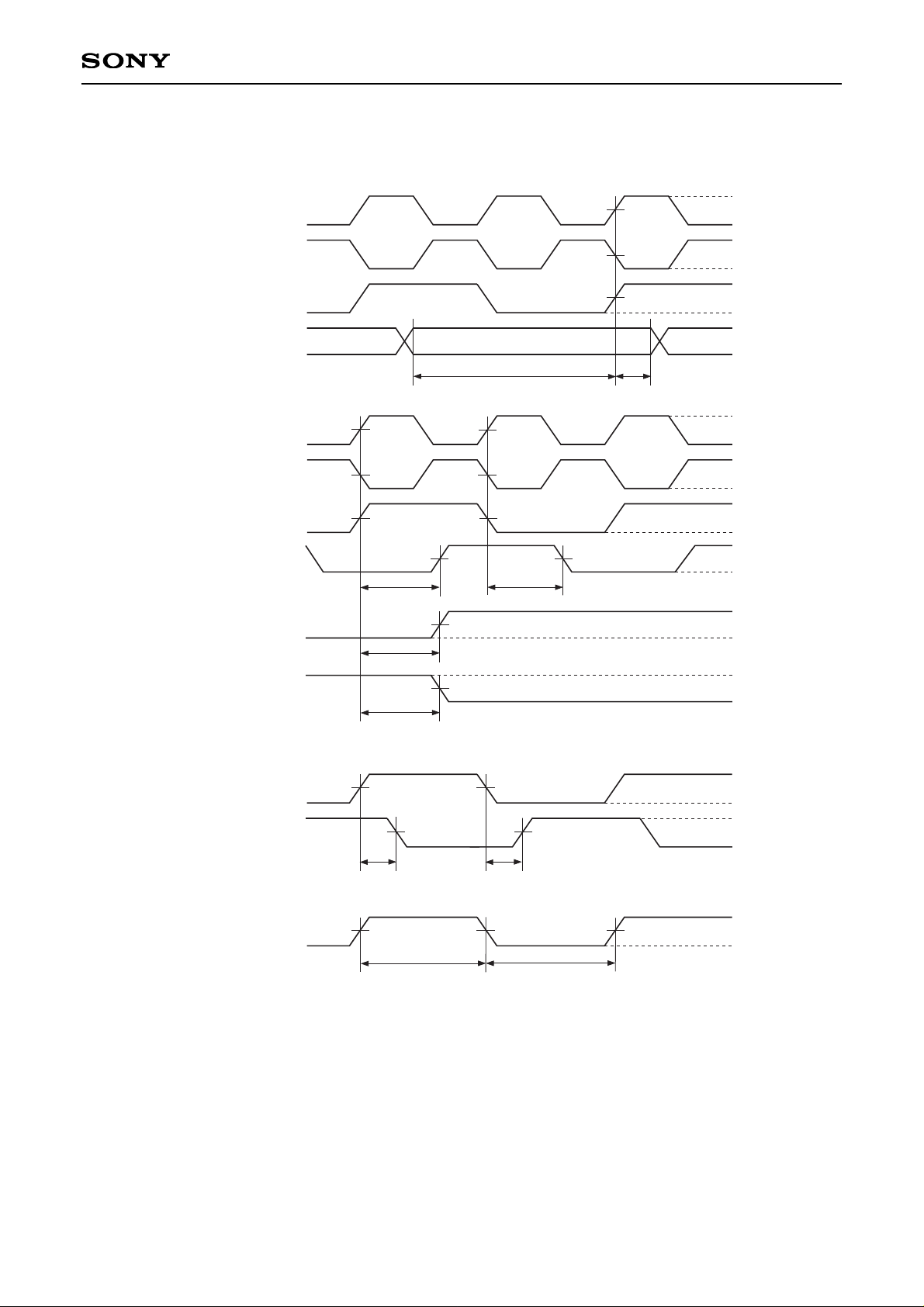
Timing Definition
CLK1P, CLK1C
CLK3P, CLK3C
CLK1N, CLK3N
VIH3
VIL3
VIH3
VIL3
0V
V
DD
VDD
50%
50%
50%
tis tih
0V
CLK2, CLK4
CLK1P, CLK1C
CLK3P, CLK3C
CLK1N, CLK3N
CLK2, CLK4
HCK1
HCK2
HCK1, HCK2
CLKOUT
RGB input, OSD input,
HDIN1, VDIN1, HDIN2
Outputs other than CLKOUT
Outputs other than CLKOUT
tof
VIH3
VIL3
VIH3
VIL3
0V
0V
0V
V
DD
VDD
VDD
0V
VDD
0V
VDD
0V
VDD
0V
V
DD
50%
50%
50%
50%
tor
tor
tof
th
∆t∆t
tl
50%
50%
50%
50%
50%
50%
50%50%
50%
50% 50%50%
50%
 Loading...