

Sony CXD2453Q Datasheet

Timing Generator for LCD Panels
For the availability of this product, please contact the sales office.
Description
The CXD2453Q is a timing signal generator for
driving the LCX017AL and LCX023AL LCD panels.
This chip outputs timing signals which support XGA
signals (1024 × 768 dots) and S-XGA signals (1280 ×
1024 dots).
Features
• Supports various XGA signals (1024 × 768 dots)
having horizontal scanning frequencies of 44-69kHz
and vertical scanning frequencies of 55 to 85Hz.
• Supports S-XGA (1280 × 1024 dots) pulse
eliminator (horizontal scanning frequency of 69kHz
or less).
• Controls the sample-and-hold position of the
CXA2112R sample-and-hold driver.
• Line inversion and field inversion signal generation
• AC drive of LCD panels during no signal.
CXD2453Q
80 pin QFP (Plastic)
Absolute Maximum Ratings (VSS = 0V)
• Supply voltage VDD VSS – 0.5 to +4.0 V
• Input voltage VI
(3.3V input pin) VSS – 0.5 to VDD + 0.5 V
(5.0V input pin) VSS – 0.5 to VDD + 2.5 V
• Output voltage VO VSS – 0.5 to VDD + 0.5 V
• Storage temperature
Tstg –55 to +125 °C
Applications
LCD projectors, etc.
Structure
Silicon gate CMOS IC
Note: Company names and product names, etc.
contains in these materials are the trademarks
or registered trademarks of the respective
companies.
Recommended Operating Conditions
• Supply voltage VDD +3.0 to +3.6 V
• Operating temperature
Topr –20 to +75 °C
Sony reserves the right to change products and specifications without prior notice. This information does not convey any license by
any implication or otherwise under any patents or other right. Application circuits shown, if any, are typical examples illustrating the
operation of the devices. Sony cannot assume responsibility for any problems arising out of the use of these circuits.
– 1 –
E97425B7Y-PS

Block Diagram
78
XCLR
TST5
24
VSYNC
HSYNC
28
29
3
Direct Clear
SYNC DETECTOR
XCKI1
CKI1
4
Master Clock
(Main)
SLCK1
26
11
CKI2
21
CKI3
XCKI3
22
SLCK2
CKI4
13
30
Master Clock
(Sub)
AUX V COUNTER
CXD2453Q
9
TST2
34
TST7
35
TST8
36
TST9
74
TST11
75
TST12
TST13
76
SLHR
HRET
IRACT
CLP1
CLP2
ENB
PRG
PCG
HCK1
HCK2
HST
17
38
69
39
40
47
48
49
51
53
55
PLL COUNTER
H POSITION
COUNTER
H TIMING
GENERATOR
V POSITION
COUNTER
V TIMING
GENERATOR
LINE
CONTROLLER
ADDITIONAL
PULSE
GENERATOR
43
19
41
44
45
15
16
27
72
79
80
67
68
70
1
BLK
SLFR
VCK
VST
FRP
TST1
TST3
TST4
TST6
TST10
TST14
TST15
XVS
XHS
ORACT
SCLK
SDAT
SCTL
18
DD
6
7
SERIAL DATA I/F
8
56
57
SHPA
58
SHPB
59
SHPC
60
SHPD
INV
61
VB
62
HB
64
65
DWN
66
XRGT
RGT
12
5
2
10
ss
ss
ss
ss
V
V
V
V
14
23
20
ss
ss
ss
V
V
V
25
37
31
ss
ss
V
V
50
42
ss
ss
ss
V
V
V
52
63
71
54
ss
ss
V
V
77
ss
ss
V
V
V
32
VDD
33
VDD
VDD
46
73
VDD
ss
V
– 2 –
Pin Description
CXD2453Q
Pin
No.
1
2
3
4
5
6
7
8
9
10
11
12
13
14
15
Symbol I/O Description
TST1
VSS
—
Test pin (Not connected.)
—
GND
CKI1
I
Master clock input 1 (differential)
XCKI1
VSS
SCLK
SDAT
SCTL
TST2
VSS
CKI2
VSS
CKI4
VSS
TST3
—
GND
I
Serial data clock input
I
Serial data input
I
Serial data control signal input
—
Test pin (connect to GND)
—
GND
I
Master clock input 2
—
GND
I
Master clock input 4
—
GND
—
Test pin (Not connected.)
Input pin for
open status
—
—
—
—
—
—
—
—
—
—
—
—
—
—
16
17
18
19
20
21
22
23
24
25
26
27
28
29
30
31
32
TST4
SLHR
VDD
SLFR
VSS
CKI3
XCKI3
VSS
TST5
VSS
SLCK1
TST6
VSYNC
HSYNC
SLCK2
VSS
VDD
—
Test pin (Not connected.)
I
Reset by HSYNC of PLL counter (High: Disabled, Low: Enabled)
—
Power supply
I
FRP polarity inversion cycle selection (High: Field inversion, Low: Line inversion)
—
GND
I
Master clock input 3 (differential)
—
GND
—
Test pin (Not connected.)
—
GND
I
Clock input selection 1 (High: CKI2, Low: CKI1)
—
Test pin (Not connected.)
I
Vertical sync signal input
I
Horizontal sync signal input
I
Clock input selection 2 (High: CKI4, Low: CKI3)
—
GND
—
Power supply
—
H
—
L
—
—
—
—
—
L
—
—
—
L
—
—
33
34
35
36
VDD
TST7
TST8
TST9
—
Power supply
—
Test pin (connect to VDD)
—
Test pin (connect to VDD)
—
Test pin (connect to VDD)
—
—
—
—
– 3 –
CXD2453Q
Pin
No.
37
38
39
40
41
42
43
44
45
46
47
48
49
50
51
Symbol I/O Description
VSS
HRET
CLP1
CLP2
VCK
VSS
BLK
VST
FRP
VDD
ENB
PRG
PCG
VSS
HCK1
—
GND
O
Phase comparison pulse output
O
Pedestal clamp pulse 1 output
O
Pedestal clamp pulse 2 output
O
V clock pulse output
—
GND
O
BLK pulse output
O
V start pulse output
O
AC drive inversion pulse output
—
Power supply
O
ENB pulse output
O
PRG pulse output
O
PCG pulse output
—
GND
O
H clock 1 pulse output
Input pin for
open status
—
—
—
—
—
—
—
—
—
—
—
—
—
—
—
52
53
54
55
56
57
58
59
60
61
62
63
64
65
66
67
68
VSS
HCK2
VSS
HST
SHPA
SHPB
SHPC
SHPD
INV
VB
HB
VSS
DWN
XRGT
RGT
XVS
XHS
—
GND
O
H clock 2 pulse output
—
GND
O
H start pulse output
O
External sample-and-hold driver control signal output
O
External sample-and-hold driver control signal output
O
External sample-and-hold driver control signal output
O
External sample-and-hold driver control signal output
O
External sample-and-hold driver control signal output
O
VB signal output
O
HB signal output
—
GND
O
Up/down inversion signal output
O
Left/right inversion signal (reverse polarity) output
O
Left/right inversion signal output
O
Auxiliary pulse output
O
Auxiliary pulse output
—
—
—
—
—
—
—
—
—
—
—
—
—
—
—
—
—
69
70
71
72
IRACT
ORACT
VSS
TST10
O
Auxiliary pulse output
O
Auxiliary pulse output
—
GND
—
Test pin (Not connected.)
—
—
—
—
– 4 –

CXD2453Q
Pin
No.
73
74
75
76
77
78
79
80
Symbol I/O Description
VDD
TST11
TST12
TST13
VSS
XCLR
TST14
TST15
—
Power supply
—
Test pin (connect to VDD)
—
Test pin (connect to VDD)
—
Test pin (connect to VDD)
—
GND
I
System clear (Low: All clear)
—
Test pin (Not connected.)
—
Test pin (Not connected.)
∗
H: Pull-up, L: Pull-down
Input pin for
open status
—
—
—
—
—
H
—
—
Electrical Characteristics
• DC characteristics (Topr = –20 to +75°C, VSS = 0V)
Item
Supply voltage
Symbol
VDD
Conditions
—
Min. Typ. Max. Unit
3.0
3.3
3.6
Applicable pins
—
Input voltage 1
Input voltage 2
Input voltage 3
Input voltage 4
Output voltage 1
Output voltage 2
Output voltage 3
VIH1
VIL1
VIH2
VIL2
VIH3
VIL3
VC
(center
level)
∗1
VIH4
∗1
VIL4
VOH
VOL
VOH
VOL
VOH
VOL
3.3V CMOS input
5.0V CMOS input
5.0V CMOS
Schmitt trigger input
Low amplitude
differential input
IOH = –4mA
IOL = 4mA
IOH = –8mA
IOL = 8mA
IOH = –12mA
IOL = 12mA
0.65VDD
VSS
0.65VDD
VSS
0.8VDD
VSS
(VDD ×
0.606)
– 0.1
VIL4 + 0.3
VSS
VDD – 0.5
VSS
VDD – 0.5
VSS
VDD – 0.5
VSS
—
—
—
—
—
—
VDD ×
0.606
—
—
—
—
—
—
—
—
VDD
0.25VDD
VDD + 1.9
0.25VDD
VDD + 1.9
0.2VDD
(VDD ×
0.606)
+ 0.1
VDD
VIH4 – 0.3
VDD
0.4
VDD
0.4
VDD
0.4
SLHR, SLFR,
XCLR, SLCK1/2
CKI2, CKI4
SCLK, SDAT, SCTL,
VSYNC, HSYNC
V
CKI1/XCKI1,
CKI3/XCKI3
∗2
VCK, BLK, VST,
ENB, PCG
HCK1, HCK2,
HST
Input pull-up/pulldown resistance
Current
consumption
∗1
VIH4 > (max. value of VC) and VIL4 < (min. value of VC)
∗2
Output pins other than those indicated in items output voltage 2 and output voltage 3.
RP
IDD
Pull-up VI = 0V
Pull-down VI = VDD
Master clock = 95MHz
VDD = 3.3V
Output load = 30pF
25
—
50
—
200
40
– 5 –
SLHR, XCLR
kΩ
SLFR, SLCK1/2
mA
—
CXD2453Q
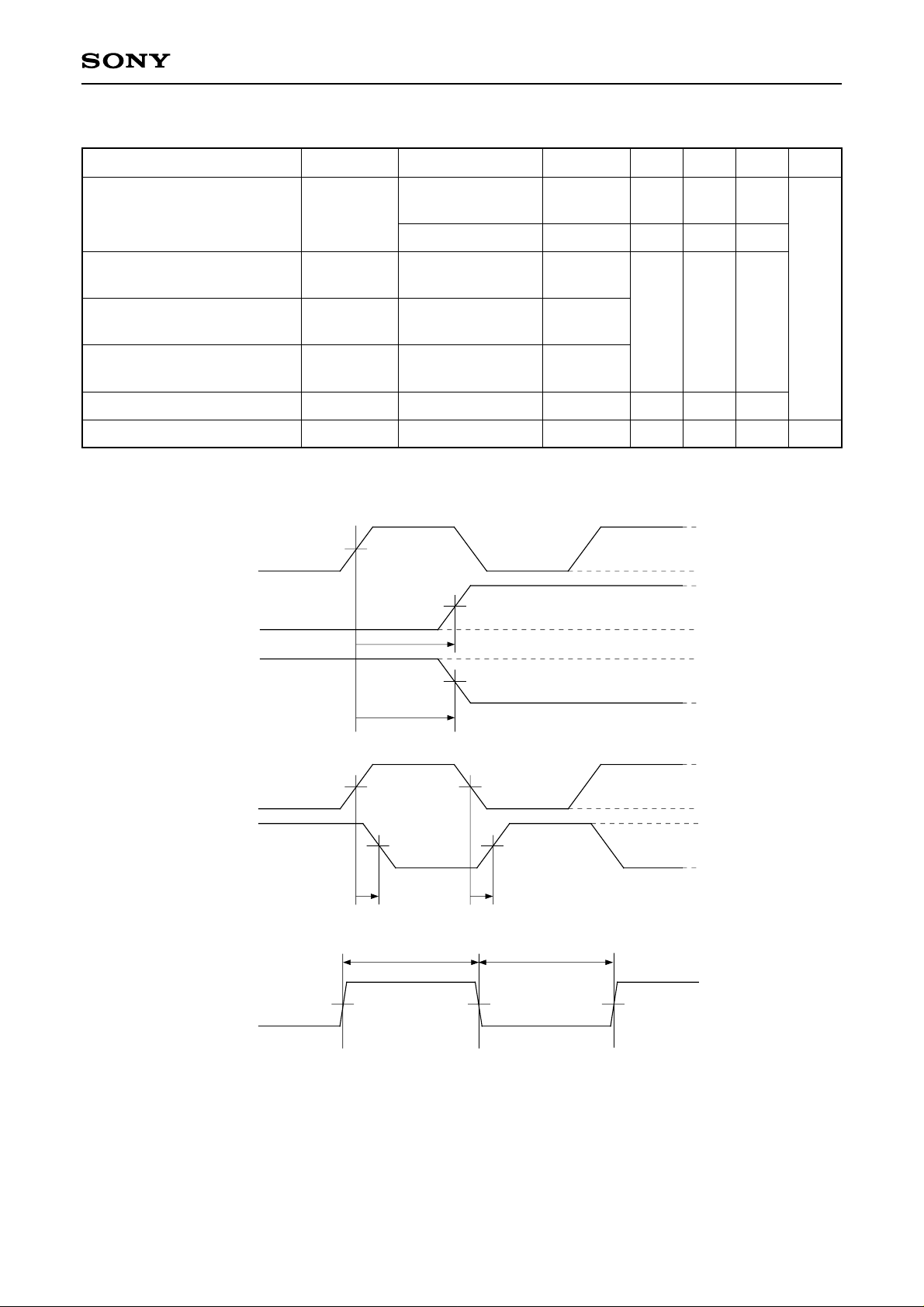
• AC characteristics (Topr = –20 to +75°C, VDD = 3.3V ± 0.3V, VSS = 0V)
Item
Clock input cycle
Output rise/fall delay time
Output rise/fall delay time
Output rise/fall delay time
Cross-point time difference
Duty ratio
Timing Definitions
CKI1, CKI2,
CKI3, CKI4
Output
Output
Symbol Applicable pins Conditions Min. Typ. Max. Unit
—
tpr/tpf
tpr/tpf
tpr/tpf
∆t
tH/ (tH + tL)
50%
CKI1/XCKI1,
CKI3/XCKI3
CKI2, CKI4
HCK1, HCK2, HST
VCK, BLK, VST,
ENB, PCG
Other output pins
HCK1, HCK2
HCK1, HCK2
50%
tpr
50%
tpf
—
—
CL = 90pF
CL = 50pF
CL = 30pF
CL = 90pF
CL = 90pF
10.5
10.5
—
–5
48
—
—
—
—
50
VDD
0V
V
DD
0V
DD
V
0V
—
—
25
5
52
ns
%
HCK1
HCK2
HCK1, HCK2
50%
50%
∆t ∆t
t
H tL
50%
50%
50%50% 50%
DD
V
0V
VDD
0V
– 6 –
CXD2453Q
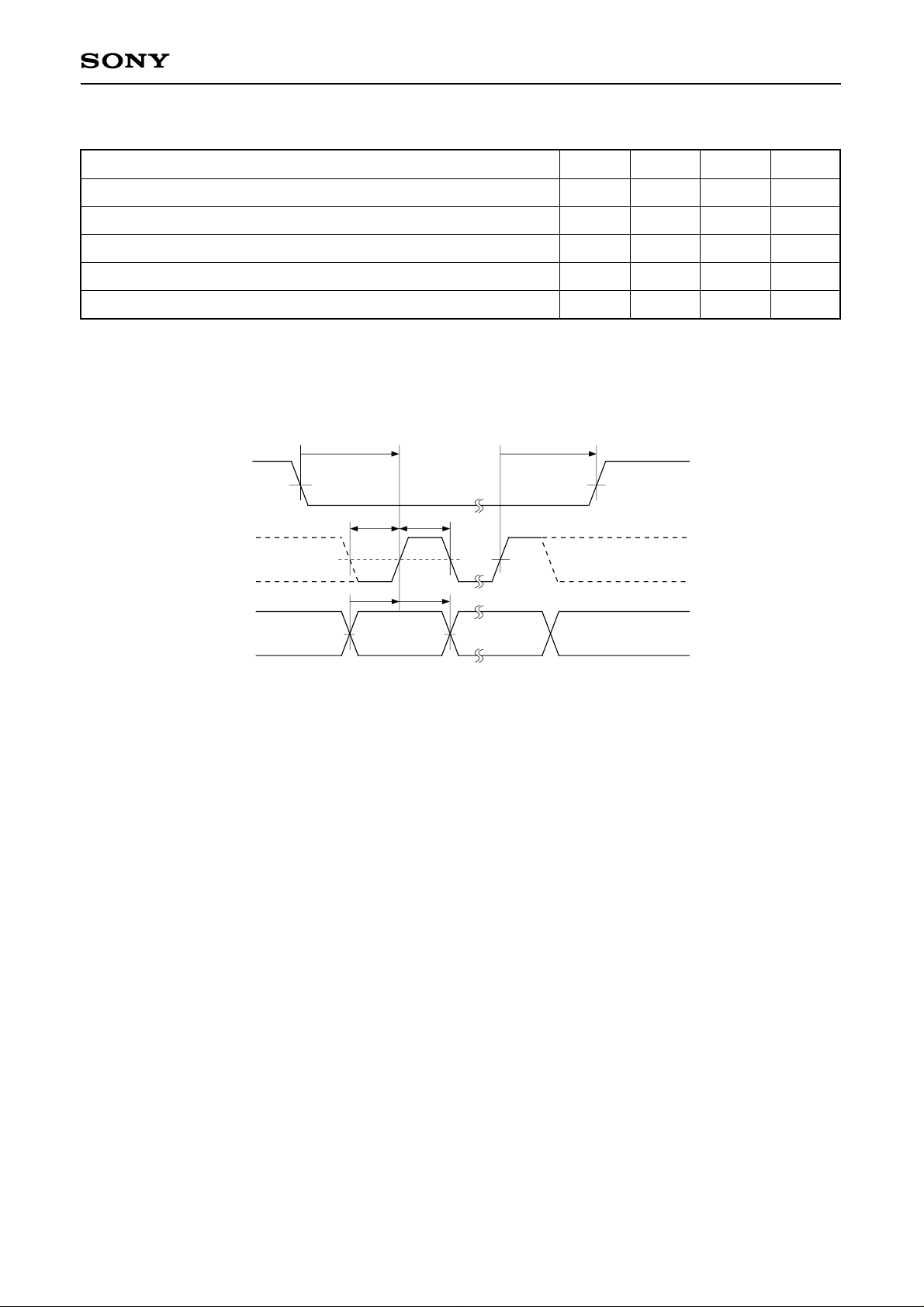
Serial Interface AC Characteristics (Topr = –20 to +75°C, VDD = 3.3V ± 0.3V, VSS = 0V)
Item Symbol Min. Typ. Max.
SCTL setup time with respect to rise of SCLK
ts0
8T
∗3
—
—
SCTL hold time with respect to rise of SCLK
SDAT setup time with respect to rise of SCLK
SDAT hold time with respect to rise of SCLK
SCLK pulse width
∗3
T: Master clock cycle (ns)
Timing Definitions
t
s0
SCTL
SCLK
SDAT
50%
50%
50%
t
w1tw1
ts1th1
(D15) (D0)
50%
50%
th0
ts1
th1
tw1
t
h0
50%
8T
4T
4T
4T
—
—
—
—
—
—
—
—
– 7 –
 Loading...