

Sony CXD2452R Datasheet
– 1 –
CXD2452R
E96830C9X
Timing Generator for Progressive Scan CCD Image Sensor
Description
The CXD2452R is a timing generator which generates
the timing pulses for performing progressive scan
readout for digital still cameras and personal
computer image input applications using the
ICX098AK CCD image sensor.
Features
• Base oscillation frequency 36.81MHz (2340fH)
• Monitoring readout allowed
• High-speed/low-speed electronic shutter function
• Horizontal driver for CCD image sensor
• Signal processor IC system clock generation 1170fH,
780fH
• Vertical/horizontal sync (SSG) timing generation
Applications
• Digital still cameras
• Personal computer image input
Structure
Silicon gate CMOS IC
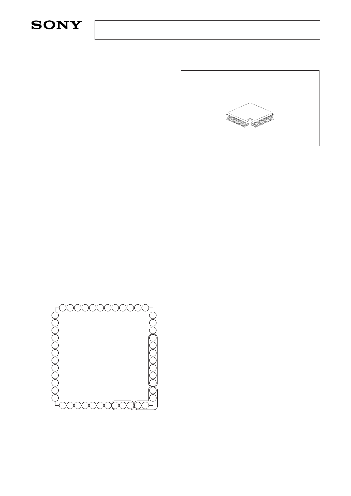
Pin Configuration
Absolute Maximum Ratings
• Supply voltage VDD Vss – 0.5 to +7.0 V
• Input voltage VI Vss – 0.5 to VDD + 0.5 V
• Output voltage VO Vss – 0.5 to VDD + 0.5 V
• Operating temperature
Topr –20 to +75 °C
• Storage temperature
Tstg –55 to +150 °C
Recommended Operating Conditions
• Supply voltage
VDDa, VDDb, VDDc, VDDd 3.0 to 3.6 V
• Operating temperature
Topr –20 to +75 °C
Applicable CCD Image Sensors
ICX098AK (Type 1/4 CCD)
Sony reserves the right to change products and specifications without prior notice. This information does not convey any license by
any implication or otherwise under any patents or other right. Application circuits shown, if any, are typical examples illustrating the
operation of the devices. Sony cannot assume responsibility for any problems arising out of the use of these circuits.
48 pin LQFP (Plastic)
2
3
4
5
6
7
8
9
10
11
12
13
14
15
16
17
18
19
20
21
22
23
24
25
2627
28
29
30
40
39
38
37
36
35
34
31
32
33
41
42
43
44
45
46
47
48
1
OSCI
3MCK
V
SS
1
WEN
TEST
V
DD
1
XCLPOB
H1
V
SS
2
RG
V
DD
2
V
SS
5
CLD
FRI
HRI
HRO
FRO
EBCKSM
SEN
SSK
SSI
V
DD
6
RST
OSCO
XV1
V
DD7
XSUB
XV2
XSG2
XV3
V
SS6
MCK
DSGAT
H2
V
DD3
V
DD4
XSHP
XSHD
V
SS4
1/2MCK
ID
V
SS
3
XCLPDM
XRS
V
DD5
PBLK
XSG1
3/2MCK
*Groups of pins enclosed in the fingure indicate sections for which power supply separationis possible.
– 2 –
CXD2452R
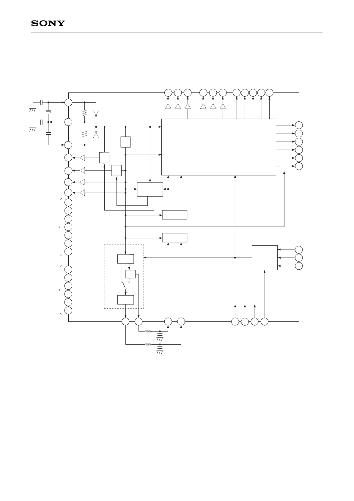
Block Diagram
3
4
7
15
21
30
40
37
34
31
33
WEN
TEST
XCLPDM
XCLPOB
12
H1
9
RG
RST
FRI
HRI
HRO
FRO
EBCKSM
SEN
SSK
SSI
XSUB
DSGAT
13
H2
ID
17
18
19
XSHP
XSHD
XRS
PBLK
41
42
43
44
46
XV1
XV2
XSG2
XV3
XSG1
Latch
27
28
29
Latch
Latch
HRI
differential
1/2
1/3
1/2
1/390
1/525
SSG
32
5
Register
Pulse Generator
2
8
10
11
14
16
20
24
26
39
38
35
45
47
48
1
OSCI
3MCK
V
SS
CLD
V
DD
1/2MCK
OSCO
MCK
36
6
25
3/2MCK
23
1/2
22
– 3 –
CXD2452R
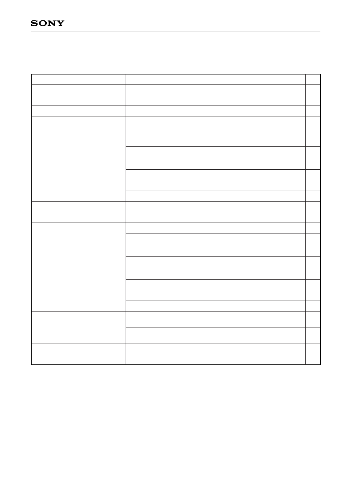
Pin Description
Pin
No.
1
2
3
4
5
6
7
8
9
10
11
12
13
14
15
16
17
18
19
20
21
22
23
24
25
26
27
28
29
30
31
3MCK
Vss1
WEN
ID
TEST
VDD1
XCLPOB
VDD2
RG
Vss2
Vss3
H1
H2
VDD3
XCLPDM
VDD4
XSHP
XSHD
XRS
Vss4
PBLK
1/2MCK
3/2MCK
VDD5
RST
VDD6
SSI
SSK
SEN
EBCKSM
FRO
I
—
O
O
I
—
O
—
O
—
—
O
O
—
O
—
O
O
O
—
O
O
—
—
I
—
I
I
I
I
O
Internal main clock. (2340fH)
GND
Memory write timing.
Stop control possible using the serial interface data.
Vertical direction line identification pulse output.
Stop control possible using the serial interface data.
IC test pin; normally fixed to GND. (With pull-down resistor)
3.3V power supply. (Power supply for common logic block)
CCD optical black signal clamp pulse output.
Stop control possible using the serial interface data.
3.3V power supply. (Power supply for RG)
CCD reset gate pulse output. (780fH)
GND
GND
CCD horizontal register drive clock output. (780fH)
CCD horizontal register drive clock output. (780fH)
3.3V power supply. (Power supply for H1/H2)
Pulse output for dummy bit block clamp .
3.3V power supply. (Power supply for CDS system)
Precharge level sample-and-hold pulse output. (780fH)
Data level sample-and-hold pulse output. (780fH)
Sample-and-hold pulse output for analog/digital conversion phase alignment. (780fH)
GND
Pulse output for horizontal and vertical blanking interval pulse cleaning.
Horizontal direction pixel identification pulse output.
Stop control possible using the serial interface data.
System clock output for signal processing IC (1170fH).
Stop control possible using the serial interface data.
3.3V power supply. (Power supply for common logic block)
Internal system reset input. High: Normal status, Low: Reset status
Always input one reset pulse after power-on.
3.3V power supply. (Power supply for common logic block)
Serial interface data input for internal mode settings.
Serial interface clock input for internal mode settings.
Serial interface strobe input for internal mode settings.
CHKSUM enable. (With pull-down resistor)
High: Sum check invalid, Low: Sum check valid
Vertical sync signal output.
Stop control possible using the serial interface data.
Symbol I/O Description
– 4 –
CXD2452R
32
33
34
35
36
37
38
39
40
41
42
43
44
45
46
47
48
HRO
HRI
FRI
CLD
VSS5
DSGAT
MCK
Vss6
XSUB
XV3
XSG2
XSG1
XV2
VDD7
XV1
OSCO
OSCI
O
I
I
O
—
I
O
—
O
O
O
O
O
—
O
O
I
Horizontal sync signal output.
Stop control possible using the serial interface data.
Horizontal sync signal input.
Vertical sync signal input.
Clock output for analog/digital conversion IC. (780fH)
Phase adjustment in 60° units possible using the serial interface data.
GND
Control input used to stop pulse generation for CCD image sensor, sample-and-
hold IC and analog/digital conversion IC. High: Normal status, Low: Stop status
Controlled pulse can be changed using the serial interface data.
System clock output for signal processor IC. (780fH)
GND
Pulse output for electronic shutter.
CCD vertical register drive pulse output.
CCD sensor readout pulse output.
CCD sensor readout pulse output.
CCD vertical register drive pulse output.
3.3V power supply. (Power supply for common logic block)
CCD vertical register drive pulse output.
Inverter output for oscillation.
Inverter input for oscillation.
Pin
No.
Symbol I/O Description
– 5 –
CXD2452R
Electrical Characteristics
DC Characteristics
(Within the recommended operating conditions)
Item Pins
Symbol
Conditions Min. Typ. Max. Unit
∗1
These input pins do not have protective diodes on the internal power supply side.
∗2
These input pins have internal pull-down resistors.
∗3
The above table indicates the condition for 3.3V drive.
Supply voltage 1
Supply voltage 2
Supply voltage 3
Supply voltage 4
Input voltage 1
∗1
Input
voltage 2
∗1 ∗2
Input
voltage 3
∗2
Output
voltage 1
Output
voltage 2
Output
voltage 3
Output
voltage 4
Output
voltage 5
Output
voltage 6
Output
voltage 7
VDD2
VDD3
VDD4
VDD1, VDD5,
VDD6, VDD7
RST, DSGAT,
SSI, SSK, SEN,
FRI, HRI
EBCKSM
TEST
RG
H1, H2
XSHP, XSHD,
XRS, PBLK,
XCLPDM
3/2MCK, MCK,
CLD
1/2MCK
XV1, XV2, XV3,
XSUB, XSG1,
XSG2, XCLPOB,
ID, WEN
FRO, HRO
VDDa
VDDb
VDDc
VDDd
VIH1
VIL1
VIH2
VIL2
VIH3
VIL3
VOH1
VOL1
VOH2
VOL2
VOH3
VOL3
VOH4
VOL4
VOH5
VOL5
VOH6
VOL6
VOH7
VOL7
3.0
3.0
3.0
3.0
0.8VDDd
0.8VDDd
0.7VDDd
VDDa– 0.8
VDDb – 0.8
VDDc– 0.8
VDDd– 0.8
VDDd– 0.8
VDDd– 0.8
VDDd– 0.8
3.3
3.3
3.3
3.3
3.6
3.6
3.6
3.6
0.2VDDd
0.2VDDd
0.3VDDd
0.4
0.4
0.4
0.4
0.4
0.4
0.4
V
V
V
V
V
V
V
V
V
V
V
V
V
V
V
V
V
V
V
V
V
V
V
V
Feed current where IOH = –3.3mA
Pull-in current where IOL = 2.4mA
Feed current where IOH = –10.4mA
Pull-in current where IOL = 7.2mA
Feed current where IOH = –3.3mA
Pull-in current where IOL = 2.4mA
Feed current where IOH = –10.4mA
Pull-in current where IOL = 7.2mA
Feed current where IOH = –3.3mA
Pull-in current where IOL = 2.4mA
Feed current where IOH = –2.4mA
Pull-in current where IOL = 4.8mA
Feed current where IOH = –3.6mA
Pull-in current where IOL = 7.2mA
– 6 –
CXD2452R
Inverter I/O Characteristics for Oscillation
(Within the recommended operating conditions)
Logical Vth
Input voltage
Output voltage
Feedback resistor
Oscillation frequency
OSCI
OSCI
OSCO
OSCI, OSCO
OSCI, OSCO
LVth
VIH
VIL
VOH
VOL
RFB
f
0.7VDDd
VDDd/2
500k
20
VDDd/2
2M
0.3VDDd
VDDd/2
5M
50
V
V
V
V
V
Ω
MHz
Feed current where
IOH = –6.0mA
Pull-in current where
IOL = 6.0mA
VIN = VDDd or Vss
Inverter Input Characteristics for Base Oscillation Clock Duty Adjustment
(Within the recommended operating conditions)
Logical Vth
Input voltage
Input amplitude
3MCK
LVth
VIH
VIL
VIN
0.7VDDd
0.3
VDDd/2
0.3VDDd
V
V
V
Vp-p
fmax 50MHz sine
wave
∗1
Input voltage is the input voltage characteristics for direct input from an external source. Input amplitude is
the input amplitude characteristics in the case of input through capacitor.
Item Pins Symbol Conditions Min. Typ. Max. Unit
Item Pins Symbol Conditions Min. Typ. Max. Unit
– 7 –
CXD2452R
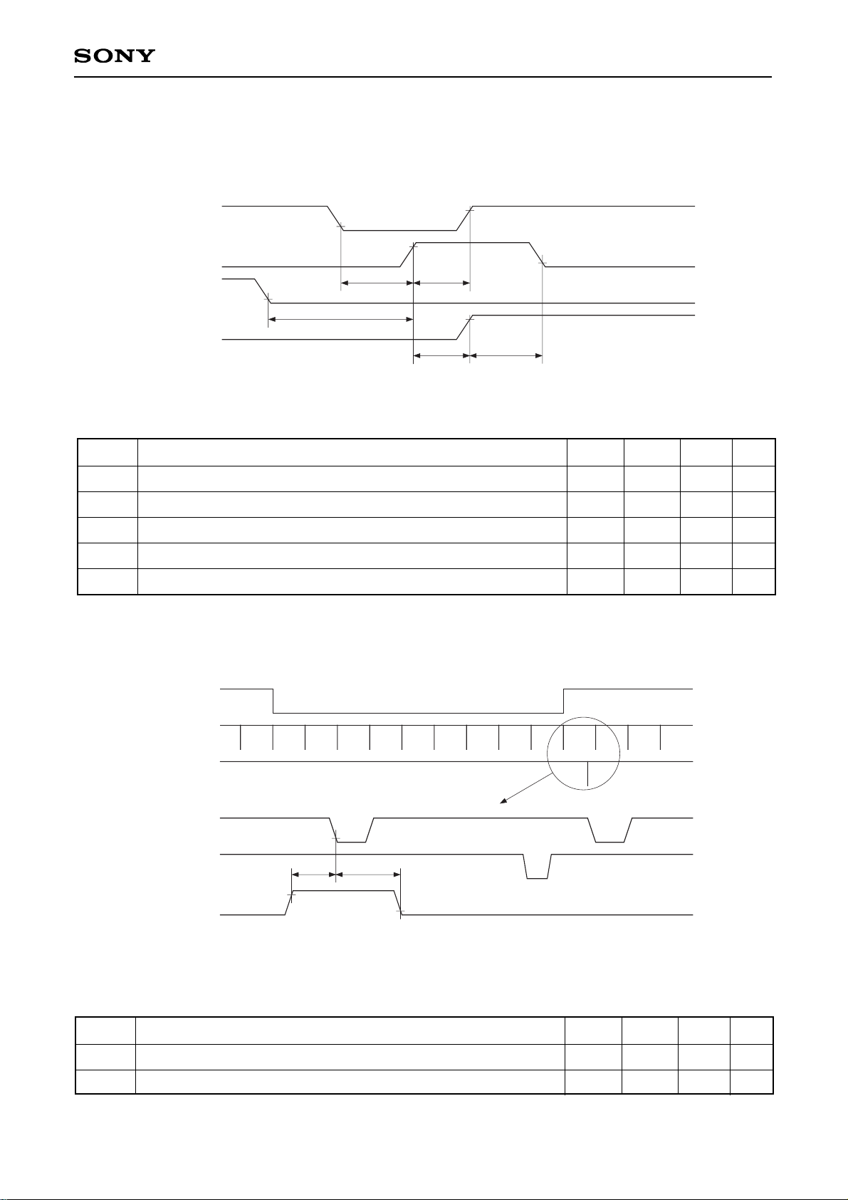
AC Characteristics
1) AC characteristics between the serial interface clocks
0.8VDDd
0.8VDDd
0.2V
DDd
0.2V
DDd
0.2V
DDd
0.8V
DDd
th1ts1
th2ts2
ts3
SSI
SSK
SEN
SEN
(Within the recommended operating conditions)
Symbol
ts1
th1
ts2
th2
ts3
SSI setup time, activated by the rising edge of SSK
SSI hold time, activated by the rising edge of SSK
SSK setup time, activated by the rising edge of SEN
SSK hold time, activated by the rising edge of SEN
SEN setup time, activated by the rising edge of SSK
20
20
20
20
20
ns
ns
ns
ns
ns
Definition Min. Typ. Max. Unit
2) Serial interface clock internal loading characteristics
0.2VDDd
0.8VDDd
th4
ts4
HRI
XSG1
SEN
0.2VDDd
FRI
HRI
XSG1
Enlarged view
Example: During recording drive mode
Note) Be sure to maintain a constantly high SEN logic level near the HRI fall immediately before XSG1
generation.
Symbol
ts4
th4
SEN setup time, activated by the falling edge of HRI
SEN hold time, activated by the falling edge of HRI
0
0
ns
ns
Definition Min. Typ. Max. Unit
(Within the recommended operating conditions)
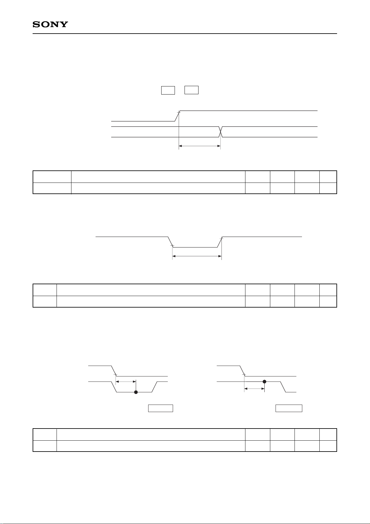
– 8 –
CXD2452R
(Within the recommended operating conditions)
Symbol
tpdPULSE
Output signal delay, activated by the rising edge of SEN
5
100
ns
Definition Min. Typ. Max. Unit
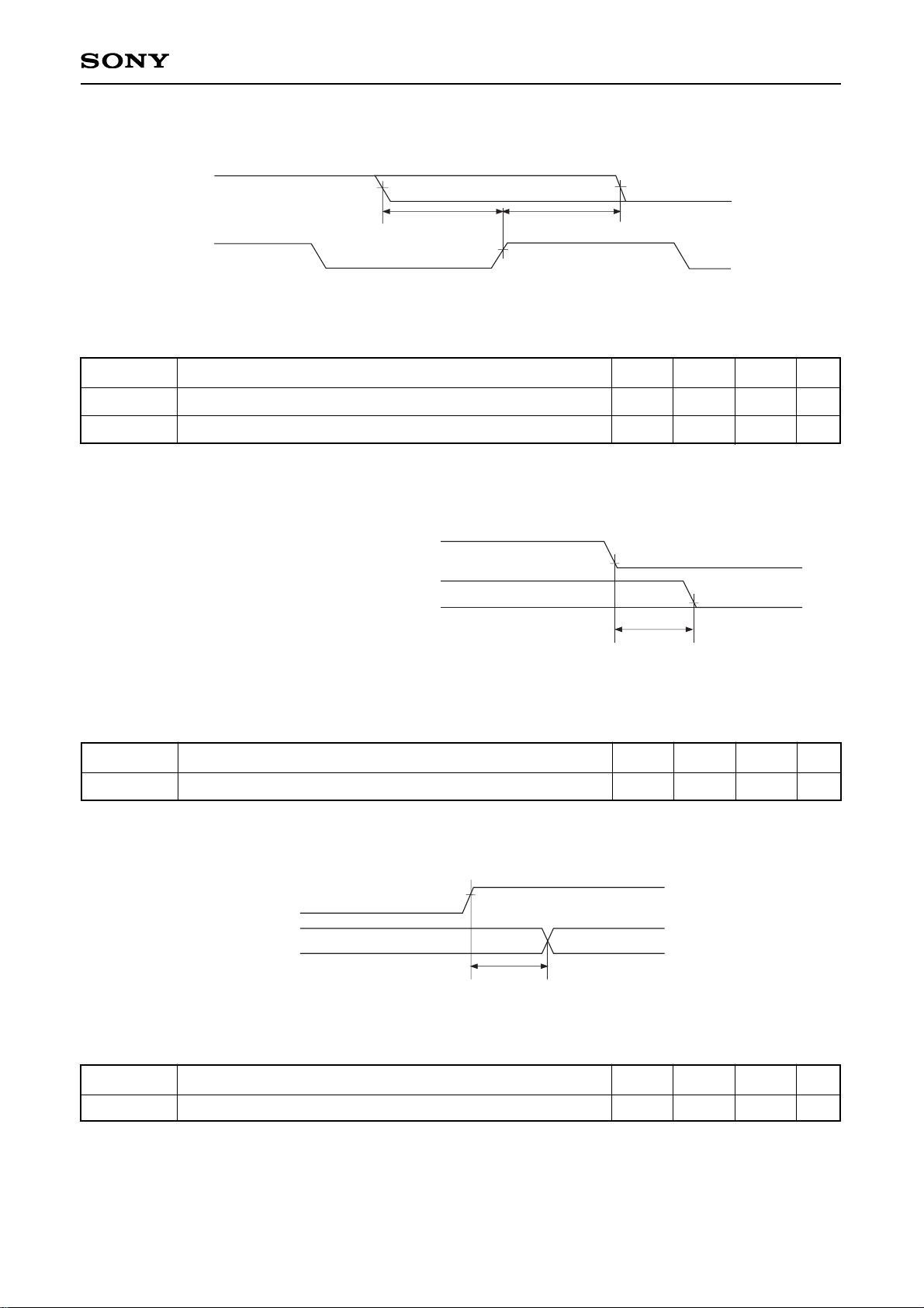
5) Phase identification characteristics using FRI and HRI input
0.2VDDd
FRI
HRI
tpd1
The field is identified as an ODD field .
0.2VDDd
FRI
HRI
tpd1
The field is identified as an EVEN field .
When the HRI logic level is low tpd1 after the
falling edge of FRI
When the HRI logic level is high tpd1 after the
falling edge of FRI
(Within the recommended operating conditions)
Symbol
tpd1
Field identification clock phase, activated by the falling edge of FRI
1100
1300
ns
Definition Min. Typ. Max. Unit
4) RST loading characteristics
0.8VDDd
tw1
0.2V
DDd
RST
(Within the recommended operating conditions)
Symbol
tw1
RST pulse width
35
ns
Definition Min. Typ. Max. Unit
3) Serial interface clock output variation characteristics
Normally, the serial interface data is loaded to the CXD2452R at the timing shown in 2) above. However, one
exception to this is when the data such as SSGSEL and STB is loaded to the CXD2452R and controlled at the
rising edge of SEN. For STB, see control data D62 to D63 STB in “Description of Operation”.
0.8VDDd
tpdPULSE
SEN
Output signal
– 9 –
CXD2452R
7) Output timing characteristics using DSGAT
tpDSGAT
0.2VDDd
0.2VDDd
DSGAT
H1, H2, RG, XV1, XV2, XV3, XSUB, XSG1, XSG2,
XSHP, XSHD, XRS, PBLK, XCLPDM, XCLPOB, CLD
H1 and H2 load capacitance = 100pF, RG load capacitance = 20pF, XV1, XV2, XV3, XSG1, XSG2, XSUB,
XSHP, XSHD, XRS, PBLK, XCLPDM, XCLPOB and CLD load capacitance = 10pF
(Within the recommended operating conditions)
Symbol
tpDSGAT
Time until the above outputs go low after the fall of DSGAT
100
ns
Definition Min. Typ. Max. Unit
6) FRI and HRI loading characteristics
FRI, HRI
MCK
0.8V
DDd
th5ts5
0.8VDDd
0.8V
DDd
MCK load capacitance = 10pF
(Within the recommended operating conditions)
Symbol
ts5
th5
FRI and HRI setup time, activated by the rising edge of MCK
FRI and HRI hold time, activated by the rising edge of MCK
10
0
ns
ns
Definition Miin. Typ. Min. Unit
8) Output variation characteristics
MCK
WEN, ID
0.8V
DDd
tpd2
Symbol
tpd2
Time until the above outputs change after the rise of MCK
20
40
ns
Definition Miin. Typ. Min. Unit
WEN and ID load capacitance = 10pF
(Within the recommended operating conditions)
 Loading...