

Sony CXD2442Q Datasheet

Timing Generator for LCD Panels
For the availability of this product, please contact the sales office.
Description
The CXD2442Q is a timing signal generator for the
SVGA LCD panel LCX016 and VGA LCD panel
LCX012BL driver. This chip has a built-in serial
interface circuit which supports various SVGA and
VGA signals as well as double-speed NTSC and
PAL signals through external control from a
microcomputer, etc.
CXD2442Q
80 pin QFP (Plastic)
Features
• Generates the LCX016/LCX012BL drive pulse.
• Supports various SVGA and VGA signals.
(LCX016/LCX012BL)
LCX016
• Aspect conversion performed at the panel side for
the 832 × 624 (Macintosh17), 800 × 600 (SVGA),
640 × 480 (VGA/NTSC), 762 × 572 (PAL),
640 × 400 (PC-98), 832 × 480 (WIDE) modes.
• Line double-speed display realized with a built-in
double-speed controller. (NTSC/PAL) (Line memory
µPD485505: NEC)
LCX012BL
• 640 × 480 (VGA/NTSC/PAL)
• Line double-speed display realized with a built-in
double-speed controller. (NTSC/PAL) (Line memory
µPD485505: NEC)
• Supports double-speed PAL pulse eliminate.
• Supports SVGA pulse eliminate.
• Supports PC-98 (640 × 400) line display.
• Generates timing signal of external sample-and-
hold circuit. (for RGB driver and high voltage drive
sample and hold)
• Supports up/down and/or right/left inversion.
• Supports 1H inversion.
• AC drive of LCD panels during no signal
Applications
LCD projectors, etc.
Structure
Silicon CMOS IC
Absolute Maximum Ratings (Ta = 25°C, VSS = 0V)
• Supply voltage VDD VSS – 0.5 to +7.0 V
• Input voltage VI VSS – 0.5 to VDD + 0.5 V
• Output voltage VO VSS – 0.5 to VDD + 0.5 V
• Operating temperature
Topr –20 to +75 °C
• Storage temperature
Tstg –55 to +150 °C
Recommended Operating Conditions
• Supply voltage VDD 4.5 to 5.5 V
• Operating temperature
Topr –20 to +75 °C
Note) "Macintosh" is a registered trademark of Apple Computer Inc..
"PC-98" is a registered trademark of NEC.
"VGA" is a registered trademark of IBM.
Other company names and product names, etc. contained in these materials are trademarks or registered
trademarks of the respective companies.
Sony reserves the right to change products and specifications without prior notice. This information does not convey any license by
any implication or otherwise under any patents or other right. Application circuits shown, if any, are typical examples illustrating the
operation of the devices. Sony cannot assume responsibility for any problems arising out of the use of these circuits.
– 1 –
E96537-ST

Block Diagram
CXD2442Q
CKI2
CKLIM
CKI1
CKO1
HSYNC
VSYNC
BLK
VCK
VST
FLDI
FLDO
FRP
XFRP
TST1
TST2
TST3
TST4
TST5
TST6
TST7
TST8
TST9
TST10
VDD: 24, 33, 48, 73 VSS: 2, 12, 17, 23, 32, 38, 42, 52, 63, 72
3
25
11
10
61
62
78
30
31
18
19
22
26
64
76
77
58
79
20
21
66
4
5
H-SYNC DETECTOR
V-SYNC SEPARATOR
V-RESET PULSE GENERATOR
V-POSITION COUNTER
PULSE ELIMINATOR
FIELD & LINE CONTROLLER
MASTER CLOCK
DECODER
&
V-TIMING PULSE
GENERATOR
DIRECT CLEAR
PLL PHASE COMPARATOR
PLL COUNTER
DECODER
V-CONTROL COUNTER
SERIAL I/F
H-POSITION COUNTER
DECODER
&
H-TIMING PULSE
GENERATOR
AUX-VD COUNTER
DECODER
74
75
13
68
69
70
71
80
14
15
16
49
50
51
53
54
67
27
28
29
34
35
36
37
39
40
41
43
44
45
46
47
55
56
57
59
60
65
7
6
9
8
1
PWM
PEO
XCLR
PRE
TC
RPD
FPD
HDN
RSTR
RCK
RSTW
WCK
HD
SCTR
SCLK
SDAT
RGT
XRGT
MODE3
MODE2
MODE1
DWN
XCLP1
XCLP2
PRG
SHD1
SHD2
SHD3
SHD4
SH1
SH2
SH3
SH4
SH5
SH6
SH7
SH8
HST
HCK1
HCK2
CLR
ENB
PCG
– 2 –
Pin Description
CXD2442Q
Pin
No.
1
2
3
4
5
6
7
8
9
10
11
12
13
14
15
Symbol
HDN
Vss
CKI2
HSYNC
VSYNC
PEO
PWM
FPD
RPD
CKO1
CKI1
Vss
TC
SCTR
SCLK
I/O Description
O
Phase comparison pulse output
—
GND
I
Clock input pin (SVGA, VGA)
I
Horizontal sync signal input pin
I
Vertical sync signal input pin
I/O
Loop filter integrator output pin (AV)
I
Loop filter integrator input pin (AV)
O
Phase comparator output pin (AV)
O
Phase comparator output pin (AV)
I/O
Oscillation cell output pin (AV)
I
Oscillation cell input pin (AV)
—
GND
I/O
FPD output pulse width adjustment pin
I
Chip select input pin (serial transfer block)
I
Serial clock input pin (serial transfer block)
Input pin for
open status
—
—
—
—
—
—
—
—
—
—
—
—
—
—
—
16
17
18
19
20
21
22
23
24
25
26
27
28
29
30
31
32
SDAT
Vss
TST1
TST2
TST3
TST4
TST5
Vss
VDD
CKLIM
TST6
XCLP1
XCLP2
PRG
FRP
XFRP
Vss
I
Serial data input pin (serial transfer block)
—
GND
—
Test pin (Not connected.)
—
Test pin (Not connected.)
—
Test pin (Not connected.)
—
Test pin (Not connected.)
—
Test pin (Connect to GND.)
—
GND
—
Power supply
I
CKI1 input limit pin (High: CKI1 input enabled, Low: Disabled)
—
Test pin (Not connected.)
O
Pedestal clamp pulse 1 output (negative polarity)
O
Pedestal clamp pulse 2 output (negative polarity)
O
Precharge signal pulse output (positive polarity)
O
AC drive inversion timing output
O
AC drive inversion timing output (reverse polarity of FRP)
—
GND
—
—
—
—
—
—
—
—
—
H
—
—
—
—
—
—
—
33
VDD
—
Power supply
—
– 3 –

CXD2442Q
Pin
No.
34
35
36
37
38
39
40
41
42
43
44
45
46
47
48
Symbol
SHD1
SHD2
SHD3
SHD4
Vss
SH1
SH2
SH3
Vss
SH4
SH5
SH6
SH7
SH8
VDD
I/O Description
O
Sample-and-hold pulse 1 output (for driver/positive polarity)
O
Sample-and-hold pulse 2 output (for driver/positive polarity)
O
Sample-and-hold pulse 3 output (for driver/positive polarity)
O
Sample-and-hold pulse 4 output (for driver/positive polarity)
—
GND
O
Sample-and-hold pulse 1 output (for high voltage drive sample and hold/positive polarity)
O
Sample-and-hold pulse 2 output (for high voltage drive sample and hold/positive polarity)
O
Sample-and-hold pulse 3 output (for high voltage drive sample and hold/positive polarity)
—
GND
O
Sample-and-hold pulse 4 output (for high voltage drive sample and hold/positive polarity)
O
Sample-and-hold pulse 5 output (for high voltage drive sample and hold/positive polarity)
O
Sample-and-hold pulse 6 output (for high voltage drive sample and hold/positive polarity)
O
Sample-and-hold pulse 7 output (for high voltage drive sample and hold/positive polarity)
O
Sample-and-hold pulse 8 output (for high voltage drive sample and hold/positive polarity)
—
Power supply
Input pin for
open status
—
—
—
—
—
—
—
—
—
—
—
—
—
—
—
49
50
51
52
53
54
55
56
57
58
59
60
61
62
63
64
65
RGT
XRGT
MODE3
Vss
MODE2
MODE1
HST
HCK1
HCK2
BLK
CLR
ENB
VCK
VST
Vss
TST7
PCG
O
Right/left inversion discrimination signal output (High: Right, Low: Left)
O
Right/left inversion discrimination signal output (High: Left, Low: Right)
O
Mode switching pin 3 output
—
GND
O
Mode switching pin 2 output
O
Mode switching pin 1 output
O
H start pulse output
O
H clock 1 pulse output
O
H clock 2 pulse output
O
BLK pulse output (positive polarity)
O
CLR pulse output (positive polarity)
O
ENB pulse output (negative polarity)
O
V clock pulse output
O
V start pulse output
—
GND
—
Test pin (Not connected.)
O
PCG pulse output (positive polarity)
—
—
—
—
—
—
—
—
—
—
—
—
—
—
—
—
—
66
67
TST8
DWN
—
Test pin (Not connected.)
O
Up/down inversion discrimination signal output (High: Down, Low: Up)
– 4 –
—
—

CXD2442Q
Pin
No.
68
69
70
71
72
73
74
75
76
77
78
79
80
Symbol
RSTR
RCK
RSTW
WCK
Vss
VDD
XCLR
PRE
TST9
TST10
FLDI
FLDO
HD
I/O Description
O
Reset read output (for high-speed line buffer/negative polarity)
O
Read clock output (for high-speed line buffer)
O
Reset write output (for high-speed line buffer/negative polarity)
O
Write clock output (for high-speed line buffer)
—
GND
—
Power supply
I
System clear pin (Low: All clear)
I
Preset pin (Preset to Macintosh17 mode when Low.)
—
Test pin (Not connected.)
—
Test pin (Not connected.)
I
Field discrimination signal input
O
Field discrimination signal output
O
HD pulse output (positive polarity)
Input pin for
open status
—
—
—
—
—
—
H
H
—
—
—
—
—
∗
H: Pull up, L: Pull down
– 5 –
CXD2442Q
Electrical Characteristics
1. DC characteristics (VDD = 5.0 ± 0.5V, VSS = 0V, Topr = –20 to + 75°C)
Item
Supply voltage
Input, output voltages
Input voltage 1
Input voltage 2
Input voltage 3
Output voltage 1
Output voltage 2
Output voltage 3
Input leak current
Output leak current
Current consumption
∗1
PRE, SCLK, SDAT, SCTR, XCLR, FLDI, CKLIM, CKI1, CKO1, CKI2, PWM, PEO
∗2
MODE1, MODE2, MODE3, HD, HDN, CLR, ENB, PRG, PCG, HST, XCLP1, XCLP2, VST, BLK, FRP,
Symbol
VDD
VI, Vo
VIH
VIL
Vt+
Vt–
Vt+ – Vt–
Vt+
Vt–
Vt+ – Vt–
VOH
VOL
VOH
VOL
VOH
VOL
II
IIL
II
IOZ
IDD
CMOS input
TTL Schmitt
trigger input
CMOS Schmitt
trigger input
IOH = –2mA
IOL = 4mA
IOH = –4mA
IOL = 8mA
IOH = –3mA
IOL = 3mA
∗4
∗6
∗8
∗10
∗12
Min.
4.5
Vss
0.7VDD
2.2
0.8VDD
VDD – 0.8
VDD – 0.8
VDD/2
–10
–40
–40
–40
Typ. Max. UnitConditions
5.0
0.4
0.6
–100
5.5
VDD
0.3VDD
0.8
0.2VDD
0.4
0.4
VDD/2
10
–240
40
40
80
V
V
V
V
V
V
V
V
µA
µA
mA
Applicable pins
∗1
HSYNC
VSYNC
TC
∗2
∗3
CKO1,
PEO
∗5
∗7
∗9
∗11
At a 30pF load
XFRP, VCK, DWN, FLDO, FPD, TC, RPD, RGT, XRGT
∗3
RSTR, RSTW, RCK, WCK, SH1, SH2, SH3, SH4, SH5, SH6, SH7, SH8, SHD1, SHD2, SHD3, SHD4,
HCK1, HCK2
∗4
Normal input pins (VIN = VSS or VDD)
∗5
HSYNC, VSYNC, SCLK, SDAT, SCTR, CKI2
∗6
Pins with pull-up resistors (VIN = VSS)
∗7
PRE, XCLR, CKLIM
∗8
Bi-directional pins (input status, VIN = VSS or VDD)
∗9
CKO1, PEO, TC
∗10
At high impedance (VIN = VSS or VDD)
∗11
RPD, FPD
∗12
fclk = 60MHz, VDD = 5.5V
– 6 –
CXD2442Q
2. AC characteristics (VDD = 5.0 ± 0.5V, Vss = 0V, Topr = –20 to +75°C)
Item
Clock input cycle
Output rise time
Output fall time
Cross-point time difference
Output rise delay time
Output fall delay time
HCK1 Duty
HCK2 Duty
Note) SHP6, 5, 4, 3, 2, 1, 0: LLLLLLL (LSB), HDN4, 3, 2, 1, 0: LLLLL (LSB), SHD2, 1, 0: HHH (LSB),
SH2, 1, 0: HLH (LSB)
The minimum value for the clock input cycle (CKI2) differs according to the mode used.
Symbol
tr
tf
∆t
tpr
tpf
tH/(tH + tL)
tL/(tH + tL)
Applicable pins
CKI1
CKI2
All outputs
All outputs
HCK1, 2
All outputs
All outputs
HCK1
HCK2
Min. Typ.
28.5
16.6
–10
48
48
Max. UnitConditions
20
20
10
15
15
52
52
CL = 30pF
CL = 30pF
CL = 30pF
CL = 30pF
CL = 30pF
CL = 30pF
CL = 30pF
ns
%
3. Serial transfer AC characteristics (VDD = 5.0 ± 0.5V, Vss = 0V, Topr = –20 to +75°C)
Symbol
ts0
ts1
th0
th1
tw1L
tw1H
tw2
tw3
SCTR setup time with respect to rise of SCLK
SDAT setup time with respect to rise of SCLK
SCTR hold time with respect to rise of SCLK
SDAT hold time with respect to rise of SCLK
SCLK pulse width
SCLK pulse width
Item Min. Typ. Max.
4Tns
2Tns
4Tns
2Tns
2Tns
2Tns
5Tns
5Tns
T: Master clock cycle (ns)
– 7 –
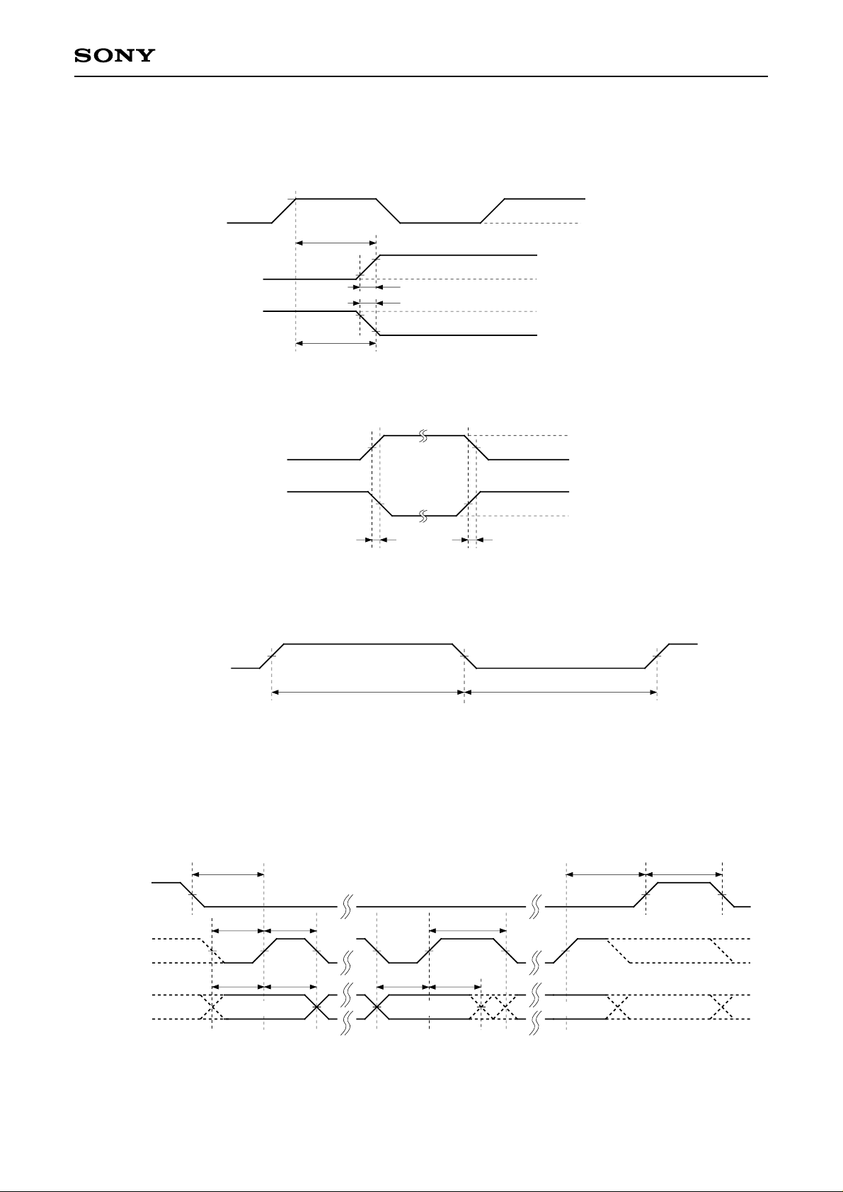
4. Timing definitions
AC characteristics
CKI1/2
Output
Output
100%
tpr
10%
90%
tpf
90%
10%
CXD2442Q
DD
V
0V
DD
V
V
0V
DD
tr
tf
0V
HCK1
HCK2
HCK1
Note) HCK2 is the reverse phase of HCK1.
Serial transfer AC characteristics
50%
50%
50% 50%
∆t
∆t
50%50% 50%
H tL
t
VDD
0V
DD
V
0V
ts0
SCTR
SCLK
SDAT
50%
50%
50%
tw1L
ts1
D15
tw1H
th1
D14
D9
ts1
D8
th1
tw2
D7
50%
D0
Note) See "Serial transfer timing" on P. 14 for the timing relationship between D15 to D0 and each pulse.
– 8 –
th0
tw3
50%
D15
CXD2442Q
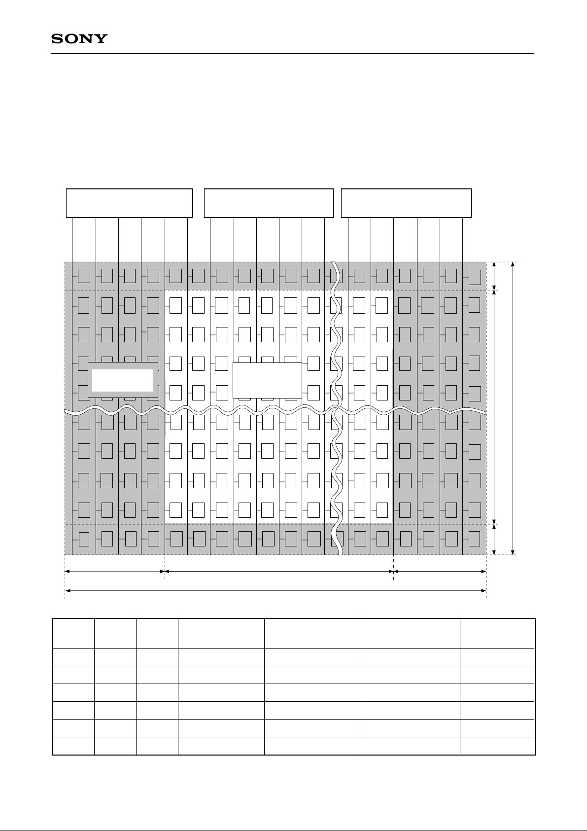
Dot Arrangement
The LCD panels supported by the CXD2442Q are the LCX016 and the LCX012BL. The dot arrangement is a
square arrangement for both panels. The shaded region in the diagram is not displayed, however, for the
LCX016, since the CXD2442Q has a built-in display area variable circuit, the number of display area dots
varies according to the mode∗1to match the various signal protocols.
LCX016 Dot Arrangement
Gate SW Gate SW Gate SW
1 dot
Photo-shielding
area
4 dots
MODE1 MODE2 MODE3 Display mode
L
L
L
Macintosh17
Display area
832 dots
840 dots
Number of horizontal
display dots
832
4 dots
Number of vertical
display dots
624
624 dots
1 dot
Number of
display dots
519,168
626 dots
L
L
L
H
H
∗1
See the description of serial data specifications for details.
L
H
H
L
L
H
L
H
L
H
SVGA
PAL
VGA/NTSC
PC-98
WIDE
– 9 –
800
762
640
640
832
600
572
480
400
480
480,000
435,864
307,200
256,000
399,360
Unit: dot
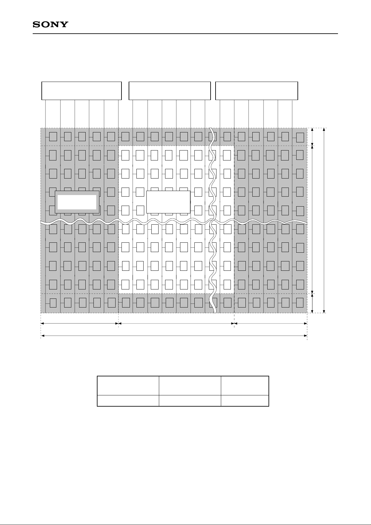
LCX012BL Dot Arrangement
Gate SW Gate SW Gate SW
CXD2442Q
1 dot
Photo-shielding
area
5 dots
Display area
644 dots
654 dots
5 dots
484 dots
486 dots
1 dot
Number of horizontal
display dots
644
Number of vertical
display dots
484
– 10 –
Number of
display dots
311,696
Unit: dot
CXD2442Q
Input Signal Protocol
1. Horizontal sync signal
a) A standard signal (HSYNC) should be input for the following display modes.
LCX016: Macintosh17 (832 × 624), SVGA (800 × 600), VGA/NTSC (640 × 480), PC-98 (640 × 400),
PAL (762 × 572), WIDE (832 × 480)
LCX012BL: VGA/NTSC/PAL (640 × 480), PC-98 (640 × 400)
However, since the CXD2442Q must be combined with a double-speed scan converter (CXD2428Q) for
NTSC/PAL double-speed display when not using the built-in double-speed controller, a double-speed
(see the CXD2428Q double-speed specifications), 1/2 cycle, 1/2 width horizontal sync signal (HSYNC)
should be input as the standard protocol signal.
b) The input sync signal polarity is not fixed, and is set by the serial data (HPOL).
2. Vertical sync signal
a) A sync-separated, normal-speed VSYNC should be input as the vertical sync signal. However, CSYNC
is also supported during NTSC/PAL display (when using the built-in double-speed controller) mode.
b) The input sync signal polarity is not fixed, and is set by the serial data (VPOL).
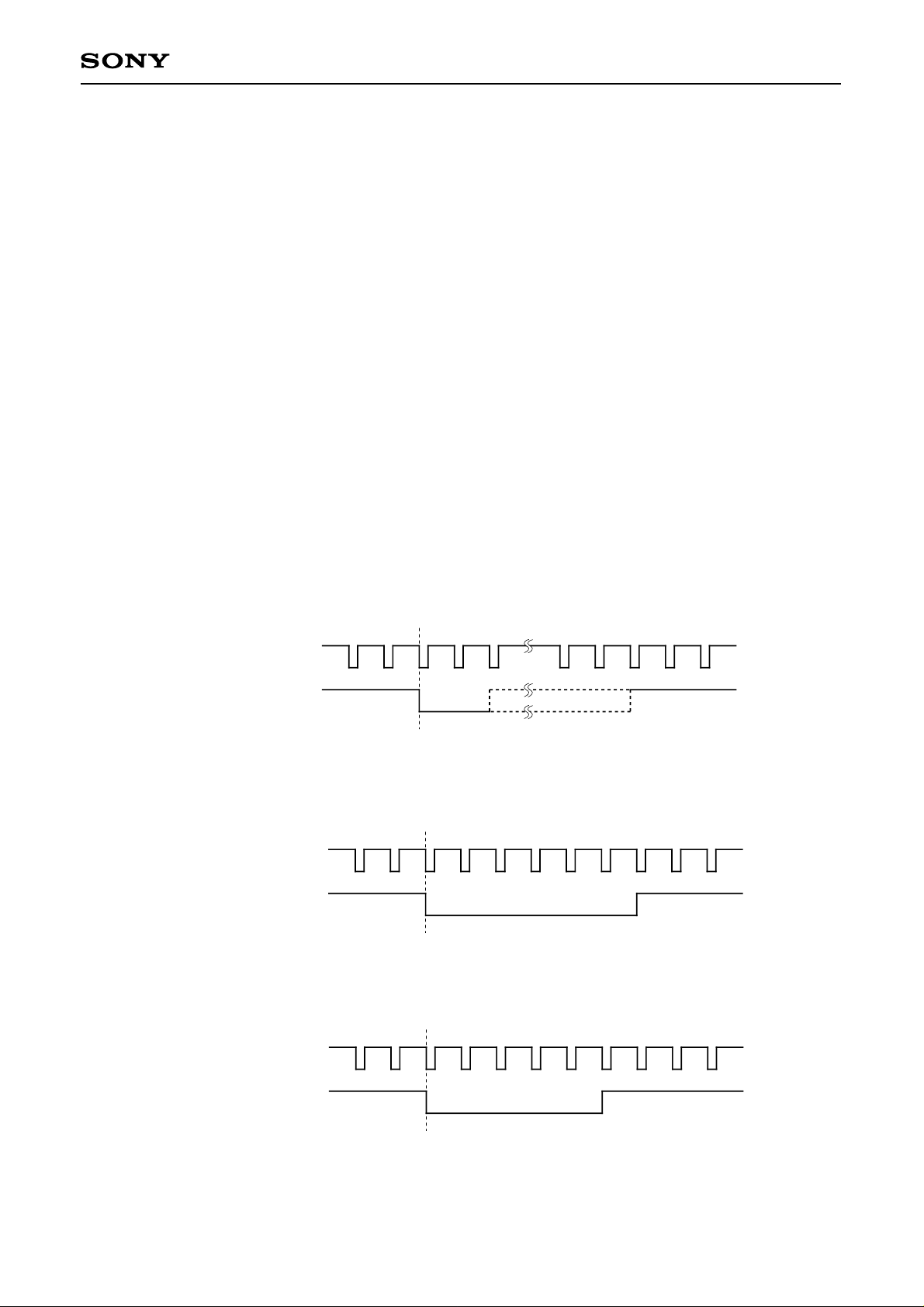
c) The phase relationship between HSYNC and VSYNC is specified as follows for the CXD2442Q.
(1) Macintosh17, SVGA, VGA, PC-98, WIDE (LCX016)/VGA, PC-98 (LCX012BL)
HSYNC
VSYNC
Sync signal phase reference
(2) Double-speed NTSC (LCX016/LCX012BL)
Double-speed HSYNC
VSYNC
Sync signal phase reference
(3) Double-speed PAL (LCX016/LCX012BL)
Double-speed HSYNC
VSYNC
Sync signal phase reference
– 11 –
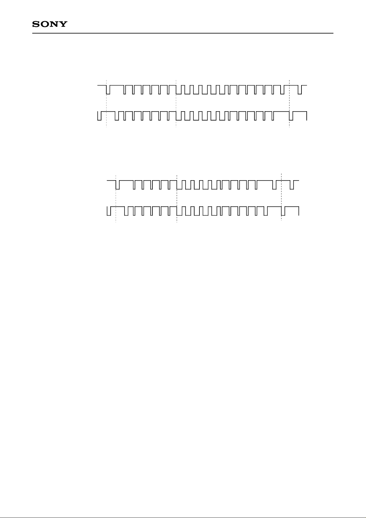
(4) NTSC (LCX016/LCX012BL)
ODD FIELD
HSYNC
VSYNC
EVEN FIELD
HSYNC
VSYNC
Sync signal phase reference
(5) PAL (LCX016/LCX012BL)
ODD FIELD
HSYNC
VSYNC
EVEN FIELD
HSYNC
VSYNC
CXD2442Q
Sync signal phase reference
Notes) (2) and (3) show the timing when using a double-speed scan converter (CXD2428Q).
(4) and (5) show the timing when using the built-in double-speed controller (CXD2442Q) and a line
memory (µPD485505: NEC)
– 12 –

CXD2442Q
Description of Operation
Sync signal input
The HSYNC and VSYNC input pins support both separate SYNC and CSYNC. When using the CXD2442Q
with CSYNC input, input CSYNC to both pins. (However, CSYNC input is supported only when using the builtin double-speed controller.)
Clock input
The CXD2442Q has two clock input pin systems to support two types of PLL circuits
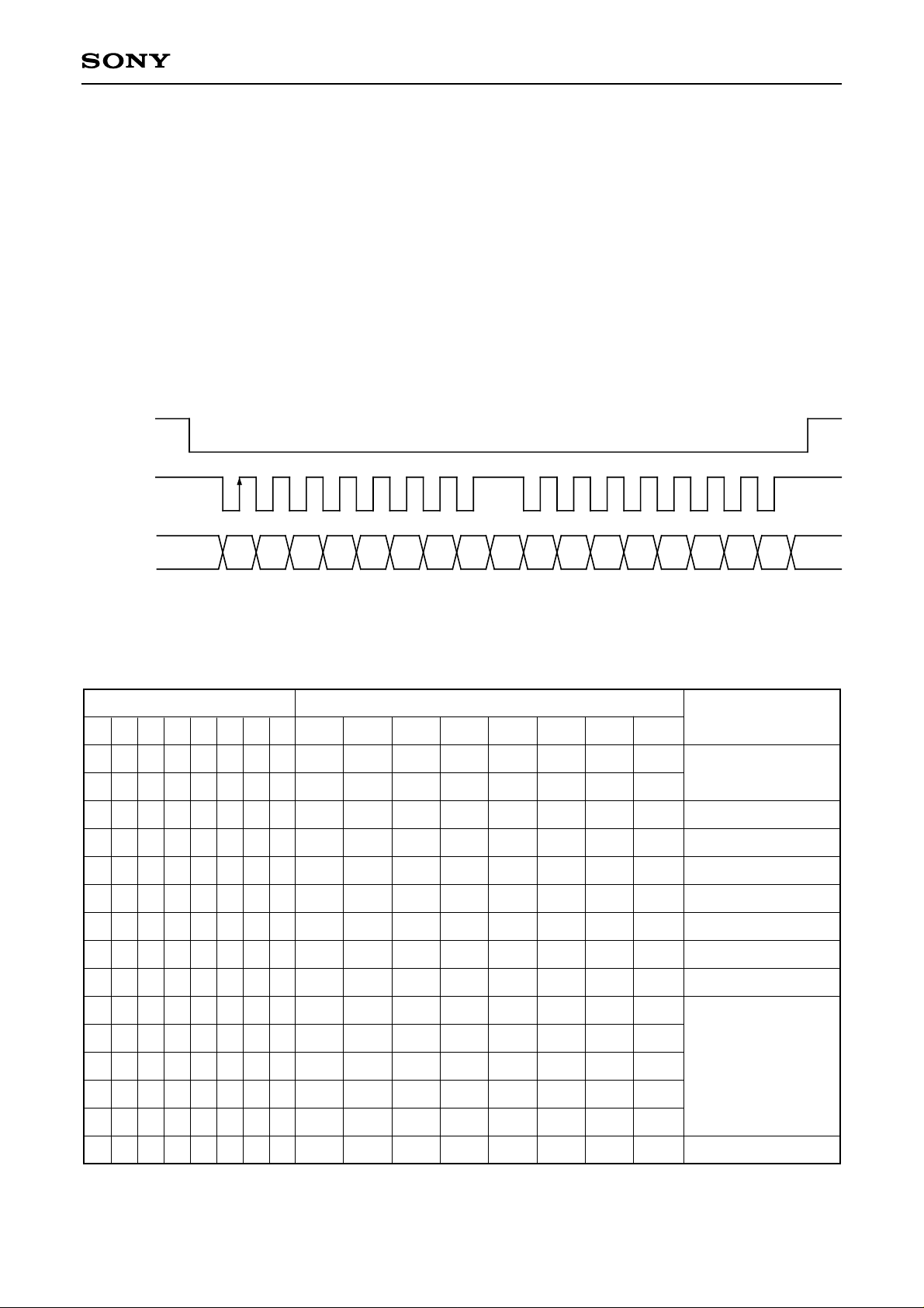
(1) CKI1 pin
A PLL circuit is comprised by the built-in phase comparator and an external VCO circuit. CKI1 is the clock
input pin when using this system, and supports the NTSC and PAL double-speed display modes (systems
which use the built-in double-speed controller). The PLL clock for this system is adjusted by setting the
RPD and FPD transition points so that they fall at the center of the windows as shown in the diagram
below. (See the Application Circuit.)
aa
HSYNC
RPD
FPD
b
500ns
b
Output waveform during PLL lock
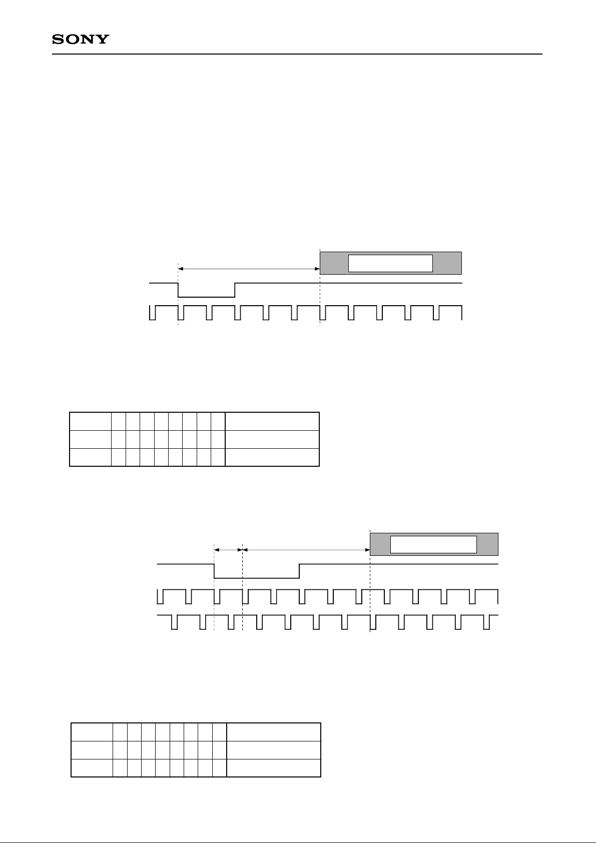
(2) CKI2 pin
This is the clock input pin when using an external PLL IC. The 1/N frequency divider output is output from
the HDN pin for the PLL IC. The HDN polarity at this time is set by the serial data HPOL.
The HDN width is calculated using the frequency division ratio N/2.
N fH
HSYNC
HDN
N/2 f
H
HPOL: L
HPOL: H
∗
fH: Master clock cycle (1 dot)
AC driving of LCD panels for no signal
The following measures have been adopted to allow AC driving of LCD panels even when there is no signal.
Horizontal direction pulse
The PLL is set to free running status. Therefore, the frequency of the horizontal direction pulse is
dependent on the PLL free running frequency.
Vertical direction pulse
The number of lines is counted by an internal counter (AUX-VD COUNTER) and the vertical direction
pulses (VST, FRP) are output at a specified cycle. For the CXD2442Q, no signal (free running) status is
judged if there is no VSYNC input for longer than the following (free running detection) periods.
Mode
NTSC
PAL
Other
V cycle for no signal
263H
313H
650H
Free running detection
468H
900H
Note) NTSC and PAL modes are the modes when using the built-in double-speed controller.
– 13 –
CXD2442Q
XCLR pin
The CXD2442Q should be forcibly reset during power on in order to initialize the serial transfer block and other
internal circuits.
Serial transfer operation
1. Control method
The CXD2442Q operation timing is controlled by serial data.
The control data is comprised of an 8-bit address and 8-bit data, and the individual data is fetched at the rise
of SCLK. This fetching operation starts from the fall of SCTR and is completed at the next rise of SCTR.
Serial Transfer Timing
SCTR
SCLK
SDAT
Address
Data
D0D1D2D3D4D5D6D7D8D9D10D11D12D13D14D15
2. Control data
When using the CXD2442Q, set the control data corresponding to each signal source according to the formats
in the table below.
Address
Data
Function
D15
D14
D13 D12
0
0
0
0
0
0
0
0
0
0
0
0
0
0
0
0
0
0
D11D10
0
0
0
0
0
0
0
0
0
0
0
0
0
0
0
0
0
0
0
0
0
0
0
0
0
0
1
D9 D8 D7 D6 D5 D4 D3 D2 D1 D0
0
0
0
—
0
0
1
PLLP7
0
1
0
HP7
0
1
1
VP7
1
0
0
—
1
0
1
—
1
1
0
—
1
1
1
—
0
0
0
—
—
PLLP6
HP6
VP6
—
SHP6
—
—
—
—
PLLP5
HP5
VP5
—
SHP5
—
—
—
—
PLLP4
HP4
VP4
HDNP4
SHP4
—
—
—
—
PLLP3
HP3
VP3
HDNP3
SHP3
HCKP3
HSTP3
—
PLLP10
PLLP2
HP2
VP2
HDNP2
SHP2
HCKP2
HSTP2
—
PLLP9
PLLP1
HP1
VP1
HDNP1
SHP1
HCKP1
HSTP1
CLPP1
PLLP8
PLLP0
HP0
VP0
HDNP0
SHP0
HCKP0
HSTP0
CLPP0
(A) PLL frequency
division ratio (1/N)
(B) H-POSITION
(C) V-POSITION
(D) HDN-POSITION
(E) SH-POSITION
(F) HCK-POSITION
(G) HST-POSITION
(H) CLP-POSITION
0
0
0
0
1
0
0
1
—
—
0
0
0
0
1
0
1
0
—
0
0
0
0
1
0
1
1
—
0
0
0
0
1
1
0
0
FRP1
0
0
0
0
1
1
0
1
CK
—
—
—
1
1
1
—
—
—
—
—
FRP0
HR
—
—
—
—
VPOL
DWN
—
—
—
MBK2
HPOL
RGT
—
—
—
MBK1
MODE
HST
—
SHD2
SH2
MBK0
MODE3
PCG
—
Note) PLLP0, HP0, VP0, HDNP0, SHP0, HCKP0, HSTP0, CLPP0: LSB
– 14 –
SHD1
SH1
MBKB
MODE2
DSP
—
SHD0
SH0
MBKA
MODE1
PC98
—
(I) Mode settings
—

CXD2442Q
Each control data is described in detail below. (A) to (I)
(A) PLLP10, 9, 8, 7, 6, 5, 4, 3, 2, 1, 0
These bits set the frequency division ratio (master clock) of the internal 1/N frequency divider for the PLL. The
data is 11 bits and the frequency division ratio can be set up to 2045. The actual frequency division ratio
should be set as follows.
Number of dots for the horizontal period – 2 = Actual number of dots set
Examples of settings for major modes are shown below.
Examples using the LCX016
1) Macintosh17 (832 × 624)
PLLP setting value = 1152 (horizontal period) – 2 → 1150 (HLLLHHHHHHL: LSB)
PLLP 10 9 8 7 6 5 4 3 2 1 0
Setting data H L L L H H H H H H L
2) SVGA (800 × 600)
PLLP setting value = 1000 (horizontal period) – 2 → 998 (LHHHHHLLHHL: LSB)
PLLP 10 9 8 7 6 5 4 3 2 1 0
Setting data L H H H H H L L H H L
3) VGA (640 × 480)
PLLP setting value = 896 (horizontal period) – 2 → 894 (LHHLHHHHHHL: LSB)
PLLP 10 9 8 7 6 5 4 3 2 1 0
Setting data L H H L H H H H H H L
4) PC-98 (640 × 400)
PLLP setting value = 848 (horizontal period) – 2 → 846 (LHHLHLLHHHL: LSB)
PLLP 10 9 8 7 6 5 4 3 2 1 0
Setting data L H H L H L L H H H L
5) NTSC WIDE (832 × 480)
PLLP setting value = 1014 (horizontal period) – 2 → 1012 (LHHHHHHLHLL: LSB)
PLLP 10 9 8 7 6 5 4 3 2 1 0
Setting data L H H H H H H L H L L
6) NTSC (640 × 480)
PLLP setting value = 1560 (horizontal period) – 2 → 1558 (HHLLLLHLHHL: LSB)
PLLP 10 9 8 7 6 5 4 3 2 1 0
Setting data H H L L L L H L H H L
7) PAL (762 × 572)
PLLP setting value = 1880 (horizontal period) – 2 → 1878 (HHHLHLHLHHL: LSB)
PLLP 10 9 8 7 6 5 4 3 2 1 0
Setting data H H H L H L H L H H L
– 15 –

Examples using the LCX012BL
1) VGA (640 × 480)
PLLP setting value = 896 (horizontal period) – 2 → 894 (LHHLHHHHHHL: LSB)
PLLP 10 9 8 7 6 5 4 3 2 1 0
Setting data L H H L H H H H H H L
2) PC-98 (640 × 400)
PLLP setting value = 848 (horizontal period) – 2 → 846 (LHHLHLLHHHL: LSB)
PLLP 10 9 8 7 6 5 4 3 2 1 0
Setting data L H H L H L L H H H L
3) NTSC, PAL (640 × 480)
PLLP setting value = 1560 (horizontal period) – 2 → 1558 (HHLLLLHLHHL: LSB)
PLLP 10 9 8 7 6 5 4 3 2 1 0
Setting data H H L L L L H L H H L
CXD2442Q
(B) HP7, 6, 5, 4, 3, 2, 1, 0
These bits set the horizontal display start position. The minimum adjustment width is 1 dot, and adjustment
of up to 256 dots with 8 bits is possible using the front edge of HSYNC as the reference.
Thp
HSYNC
Thp: Timing from the edge of HSYNC to the start of image display
Image display period
Minimum and maximum Thp setting values for each mode
LCX016
HP 76543210
Min.
H H H H H H H 185 dots 153 dots 105 dots
832 × 624 800 × 600 762 × 572 640 × 480 640 × 400 832 × 480
Max.HL L L L L L L L 440 dots 408 dots 360 dots
LCX012BL
HP 76543210
Min.
H H H H H H H 110 dots
644 × 484
Max.HL L L L L L L L 365 dots
– 16 –
(C) VP7, 6, 5, 4, 3, 2, 1, 0
These bits set the vertical display start position. The minimum adjustment width is 1H, and adjustment of
up to 256H with 8 bits is possible using the following references.
Non-interlace signal input → Front edge of VSYNC
Interlace signal input → First 1H of VSYNC
(Interlace signal input indicates NTSC or PAL double-speed display (using the built-in double-speed
controller). In this case, the image is raised or lowered by two lines on the panel side with respect to a 1H
adjustment.)
(1) Non-Interlace Mode
CXD2442Q
VSYNC
HSYNC
Minimum and maximum Tvp setting values
LCX016/LCX012BL
VP 7 6 5 4 3 2 1 0 Non-Interlace Mode
Min.
LLLLLLL 8H
Max.LH H H H H H H H 263H
(2) Interlace Mode
(a) NTSC
1H
Tvp
Tvp: Timing from the edge of VSYNC to the start of image display
Tvp
Image display period
Image display period
VSYNC
HSYNC
(ODD FIELD)
HSYNC
(EVEN FIELD)
Tvp: Timing from the first 1H of the VSYNC edge to the start of image display
Minimum and maximum Tvp setting values
LCX016/LCX012BL
VP 7 6 5 4 3 2 1 0 Interlace Mode
Min.
L L L L L L L 4.5H
Max.LH H H H H H H H 259.5H
– 17 –

(b) PAL
CXD2442Q
1H
VSYNC
HSYNC
(ODD FIELD)
HSYNC
(EVEN FIELD)
Tvp: Timing from the first 1H of the VSYNC edhe to the start of image display
Minimum and maximum Tvp setting values
LCX016/LCX012BL
VP 7 6 5 4 3 2 1 0 Interlace Mode
Min.
L L L L L L L 4.5H
Max.LH H H H H H H H 259.5H
Tvp
Image display period
– 18 –
CXD2442Q
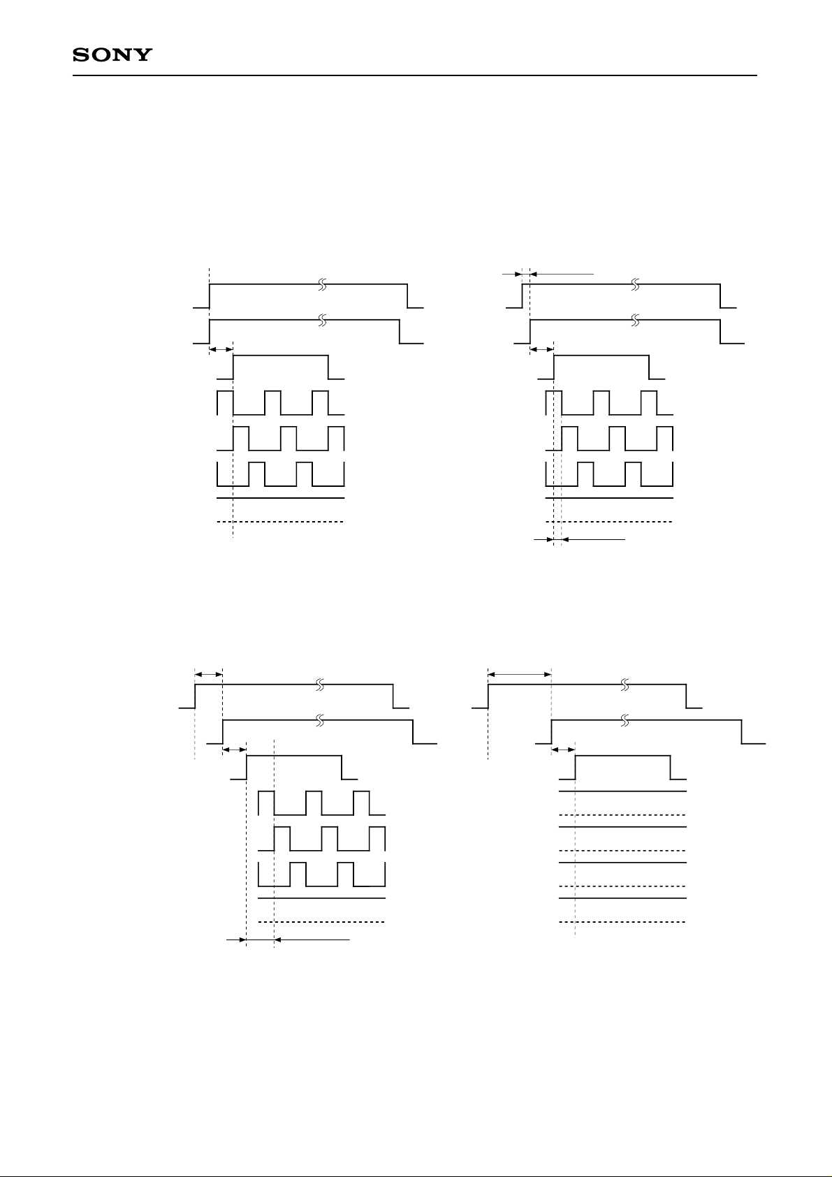
(D) HDNP4, 3, 2, 1, 0
These bits set the timing for the phase comparison pulse HDN (for the external PLL IC). The phase
relationship between the dot clock and the sync signal (HSYNC) is controlled in 3ns (Typ.) units. The control
range is 32 positions with 5 bits.
Phase control for the SH pulse (SHD4, 3, 2, 1) is also performed at the same time.
3ns (1 × 3ns)
HSYNC
HDN
HCKn
SHD1
SHD2
SHD3
SHD4
HDNP4, 3, 2, 1, 0
HSYNC
HDN
a
90ns (30 × 3ns)
a
: LLLLL
0 (decimal)
a
3ns (1 × 3ns)
: LLLLH
1 (decimal)
93ns (31 × 3ns)
a
HCKn
SHD1
SHD2
SHD3
SHD4
90ns (30 × 3ns)
HDNP4, 3, 2, 1, 0
: HHHHL
30 (decimal)
Note) The above timings assume SHD2, 1, 0: HHH and HPOL: H (serial data).
The value of a is constant regardless of the HDNP setting. n = 1, 2
– 19 –
: HHHHH
31 (decimal)
CXD2442Q
(E) SHP6, 5, 4, 3, 2, 1, 0
These bits control the phase relationship between HCK1, HCK2 and SH1, 2, 3, 4, 5, 6, 7 and 8. The phase can
be controlled in 1fH units by the upper 3 bits (SHP6, 5, 4), and in 3ns (Typ.) units by the lower 4 bits (SHP3, 2,
1, 0).
HCKn
SH1
SH2
SH3
SH4
SH5
SH6
SH7
SH8
SHP6, 5, 4, 3, 2, 1, 0
3ns (1 × 3ns)
: LLLLLLL
0 (decimal) 1 (decimal) 15 (decimal)
45ns (15 × 3ns)
: LLLHHHH: LLLLLLH
1fH (1 × 1fH)
HCKn
SH1
SH2
SH3
SH4
SH5
SH6
SH7
SH8
SHP6, 5, 4, 3, 2, 1, 0
: LLLLLLL
0 (decimal)
: LLHLLLL
1 (decimal)
Note) The above timings assume SH2, 1, 0: HLH (serial data). n = 1, 2
5f
H (5 × 1fH)
: HLHLLLL
5 (decimal)
: HHXXXXX
> 5 (decimal)
– 20 –

CXD2442Q
(F) HCKP3, 2, 1, 0
These bits control the phase relationship between the RGB signal and HCK (interlocked with HST) inside the
panel, and compensate the HCK delay for the wiring load and scanner, etc. The phase can be controlled to 15
positions (1fH increments) with 4 bits.
HST
HCK1
VCKn
A
A + (1fH × N)
HCKP3, 2, 1, 0
HST
HCK1
VCKn
HCKP3, 2, 1 ,0
: LLLL
A + (1fH × 14)
: HHHX
0 (decimal)
> 13 (decimal)
A: Timing chart timing (design specification value)
: LLLH
1 (decimal)
Note) Only HCK and HST are adjusted. The above timings assume HSTP3, 2, 1, 0: LLLH (serial data).
(G) HSTP3, 2, 1, 0
These bits control the phase relationship between HCK and HST inside the panel, and compensate the delay
difference between HST and HCK for the wiring load and scanner, etc. The phase can be controlled to 12
positions (1fH increments) with 4 bits.
HST
HCK1
1fH (1×1fH)
HSTP1, 0
HST
HCK1
HSTP1, 0
: LLLL
: HLHH 11 (decimal)
0 (dercimal)
: LLLH
12fH (12×1fH)11fH (11×1fH)
: HHXX > 11 (decimal)
1 (decimal)
Note) The above timings assume RGT: H. The HST polarity is inversed during SVGA (LCX016) mode.
– 21 –
 Loading...