

Sony CXD2424R Datasheet

CXD2424R
Timing Generator for Progressive Scan CCD Image Sensor
Description
The CXD2424R is an IC developed to generate the
timing pulses required by the Progressive Scan
CCD image sensors as well as signal processing
circuits.
Features
• CCIR support
• Electronic shutter function
• Random trigger shutter function
• Sync signal generator
• Supports external synchronization
• Supports non-interlaced operation
• Base oscillation 1888fh (29.5MHz)
Applications
Progressive Scan CCD cameras
Structure
Silicon gate CMOS IC
Absolute Maximum Ratings
• Supply voltage VDD VSS – 0.5 to +7.0 V
• Input voltage VI VSS – 0.5 to VDD + 0.5 V
• Output voltage VO VSS – 0.5 to VDD + 0.5 V
• Operating temperature Topr –20 to +75 °C
• Storage temperature Tstg –55 to +150 °C
Recommended Operating Conditions
• Supply voltage VDD 4.75 to 5.25 V
• Operating temperature Topr –20 to +75 °C
64 pin LQFP (Plastic)
Applicable CCD Image Sensors
ICX075AL, ICX075AK
Sony reserves the right to change products and specifications without prior notice. This information does not convey any license by
any implication or otherwise under any patents or other right. Application circuits shown, if any, are typical examples illustrating the
operation of the devices. Sony cannot assume responsibility for any problems arising out of the use of these circuits.
– 1 –
E95306-PS
Block Diagram
CXD2424R
RG
XH1
XH2
XSHP
XSHD
XRS
XV1
XV2
XV3
XSG
XHHG1A
XHHG1B
XHHG2
XVOG
XVHOLD
11
13
14
28
29
30
26
25
22
27
15
16
17
18
19
47
WEN
46
G
A
T
E
PBLK
XCPDM
XCPOB
ID
43
45
44
42
PULSE GENERATOR
1/2
RM
41
TG
RDM
39
OCTL
REVH
37
38
COUNTER
DECODE
REND
EXT
36
59
VDI
58
VDO
HDI
61
H-DECODER
SYNC
HDO
60
57
OUTPUT CONTROL
1/472
GATE
BLK
53
54
TEST CIRCUIT
CLD
O2FH
FLD
49
50
51
V-CONTROL
V-DECODER
1/625
CL
63
62
20
21
31
32
48
35
34
33
52
VRI
HRI
TEST1
TEST2
TEST3
TEST4
TEST8
TEST7
TEST6
TEST5
NC
64
CKI
1
2
OSCI
OSCO
29.5MHz
8
Vss
10
3
TRIG
PS
4
ED0
5
ED1
6
ED2
7
SMD1
9
SMD2
12
XSUB
23
Vss
24
DD
V
40
Vss
55
Vss
56
DD
V
– 2 –
Pin Configuration
CXD2424R
CL
CLD
O2FH
NC
FLD
BLK
V
VDD
SYNC
HDI
VDI
HDO
VDO
HRI
VRI
CKI
SS
59
49
50
51
52
53
54
55
56
57
58
60
61
62
63
64
TEST8
48
1
47
WEN
2
46
41
RDM
40
SS
V
39
OCTL
38
REVH
ID
45
PBLK
44
XCPOB
XCPDM
43
RM
42
CXD2424R (G/A)
4
3
7
6
5
9
8
10
11
REND
37
12
36
13
EXT
TEST7
35
14 15
TEST6
34
TEST5
33
16
32
31
30
29
28
27
26
25
24
23
22
21
20
19
18
17
TEST4
TEST3
XRS
XSHD
XSHP
XSG
XV1
XV2
DD
V
VSS
XV3
TEST2
TEST1
XVHOLD
XVOG
XHHG2
OSCO
OSCI
PS
ED0
ED1
ED2
SMD1
Vss
SMD2
TRIG
RG
XSUB
XH1
XH2
XHHG1B
XHHG1A
– 3 –
Pin Description
CXD2424R
Pin
No.
1
2
3
4
5
6
7
8
9
10
11
12
13
14
Symbol I/O Description
OSCO
OSCI
PS
ED0
ED1
ED2
SMD1
Vss
SMD2
TRIG
RG
XSUB
XH1
XH2
O
Inverter output for oscillation.
I
Inverter input for oscillation.
Switching for electronic shutter speed input method. (With pull-down resistor)
I
Low: Parallel input, High: Serial input
I
Shutter speed setting. Strobe input for serial mode. (With pull-up resistor)
I
Shutter speed setting. Clock input for serial input. (With pull-up resistor)
I
Shutter speed setting. Data input for serial input. (With pull-up resistor)
I
Shutter mode setting. (With pull-up resistor)
—
GND
I
Shutter mode setting. (With pull-up resistor)
I
Trigger input for random trigger shutter.
O
Reset gate pulse output.
O
CCD discharge pulse output.
O
Clock output for CCD horizontal register drive.
O
Clock output for CCD horizontal register drive.
15
16
17
18
19
20
21
22
23
24
25
26
27
28
29
30
31
XHHG1A
XHHG1B
XHHG2
XVOG
XVHOLD
TEST1
TEST2
XV3
Vss
VDD
XV2
XV1
XSG
XSHP
XSHD
XRS
TEST3
O
Clock output for transfer between CCD horizontal registers.
O
Clock output for transfer between CCD horizontal registers.
O
Clock output for transfer between CCD horizontal registers.
O
Clock output for transfer from CCD vertical register to CCD horizontal register.
O
Clock output for adjusting timing of transfer to CCD horizontal register.
O
Test output. Normally open.
O
Test output. Normally open.
O
Clock output for CCD vertical register drive.
—
GND
—
Power supply.
O
Clock output for CCD vertical register drive.
O
Clock output for CCD vertical register drive.
O
CCD sensor charge readout pulse output.
O
Precharge level sample-and-hold pulse.
O
Data sample-and-hold pulse.
O
Sample-and-hold pulse.
O
Test output. Normally open.
32
33
34
35
TEST4
TEST5
TEST6
TEST7
O
Test output. Normally open.
O
Test output. Normally open.
O
Test output. Normally open.
I
Test input. Set at Low in normal operation. (With pull-down resistor)
– 4 –
CXD2424R
Pin
No.
36
37
38
39
40
41
42
43
44
45
46
Symbol I/O Description
EXT
REND
REVH
OCTL
Vss
RDM
RM
XCPDM
XCPOB
PBLK
ID
Internal synchronization/external synchronization switching. (With pull-down resistor)
I
Low: Internal synchronization, High: External synchronization
Normal reset/direct reset switching. (With pull-down resistor)
I
Low: Normal reset, High: Direct reset
V reset/HV reset switching. (With pull-down resistor)
I
Low: V reset, High: HV reset
O2FH output control. (With pull-down resistor)
I
Low: No output, High: Output
—
GND
Normal operation/random trigger shutter switching. (With pull-down resistor)
I
Low: Normal operation, High: Random trigger shutter
Switching for output mode. (With pull-down resistor)
I
Low: Non-interlaced, High: Interlaced
O
Clamp pulse output.
O
Clamp pulse output.
O
Blanking cleaning pulse output.
O
Line identification output.
47
48
49
50
51
52
53
54
55
56
57
58
59
60
61
62
63
WEN
TEST8
CL
CLD
O2FH
NC
FLD
BLK
Vss
VDD
SYNC
HDI
VDI
HDO
VDO
HRI
VRI
O
Write enable output.
I
Test input. (With pull-down resistor)
O
fck clock output. (0°)
O
fck clock output. (180°)
O
2 fH output.
—
O
Field pulse output.
O
Composite blanking output.
—
GND
—
Power supply.
O
Composite sync output.
I
Horizontal sync signal input.
I
Vertical sync signal input.
O
Horizontal sync signal output.
O
Vertical sync signal output.
I
Horizontal reset signal input.
I
Vertical reset signal input.
64
CKI
I
2 fck clock input.
– 5 –
CXD2424R
Electrical Characteristics
DC Characteristics (VDD = 4.75 to 5.25V, Topr = –20 to +75°C)
Item
Supply voltage
Input voltage 1
(Input pins other than those below)
Input voltage 2
(Pins 7, 9, 10, 58, 59, 62, 63, and 64)
Output voltage 1
(Output pins other than those below)
Output voltage 2 (Pins 28, 29, 30,
31, 32, 33, 34, 49 and 50)
Output voltage 3
(Pins 11, 13, and 14)
Output voltage 4
(Pin 1)
Feedback resistor
Pull-up resistor
Pull-down resistor
Current consumption
Symbol Conditions Min. Typ. Max. Unit
VDD
VIH1
VIL1
VIH2
VIL2
VOH1
VOL1
VOH2
VOL2
VOH3
VOL3
VOH4
VOL4
RFB
RPU
RPD
IOH = –2mA
IOL = 4mA
IOH = –4mA
IOL = 8mA
IOH = –12mA
IOL = 12mA
IOH = –12mA
IOL = 12mA
VIN = Vss or VDD
VIL = 0V
VIN = VDD
4.75
0.7VDD
0.7VDD
–0.8
–0.8
VDD – 0.8
VDD/2
250k
5.0
1M
50k
50k
5.25
0.3VDD
0.3VDD
0.4
0.4
0.4
VDD/2
2.5M
V
V
V
V
V
V
V
V
V
V
V
V
V
Ω
Ω
Ω
VDD = 5V
IDD
ICX075AL in normal
40
mA
operating state
I/O Pin Capacitances (VDD = V = 0V, fM = 1MHz)
Item
Input pin capacitance
Output pin capacitance
Symbol Min. Typ. Max. Unit
CIN
COUT
—
—
—
—
11
9
pF
pF
– 6 –
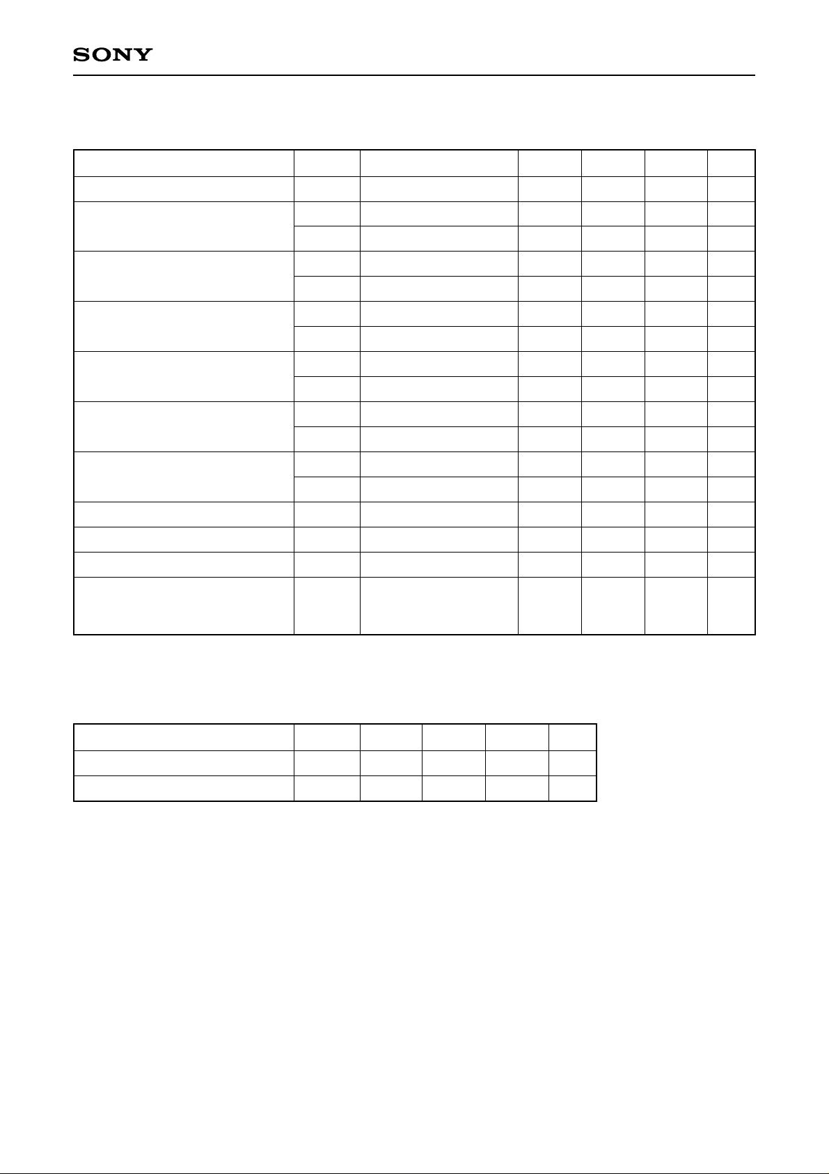
AC Characteristics
1) Phase characteristics of XH1, RG, XSHP, XSHD, XRS, CL, and CLD
tCK
CXD2424R
CK
XH1
RG
XSHP
XSHD
XRS
CL
CLD
Vpp/2
0.3VDD
0.3VDD
0.3VDD
tpd11
0.3VDD
tpd1
0.7VDD
tpd3 tpd4
tpd5
tpd7
0.3VDD
tpd9
0.3VDD
tpd12
tpd13
tpd2
0.3VDD
0.7VDD
tpd6
0.7VDD
tpd8
0.7VDD
tpd10
0.7VDD
0.7VDD
tpd14
0.7VDD
(VDD = 5.0V, Topr = 25°C, Load capacity of CL and CLD = 30pF, Load capacity of XH1, XSHP, XSHD, XRS, and RG = 10pF)
Symbol
tCK
tpd1
tpd2
tpd3
tpd4
tpd5
tpd6
tpd7
tpd8
tpd9
tpd10
tpd11
tpd12
tpd13
CK cycle
XH1 rising delay, activated by the falling edge of CK
XH1 falling delay, activated by the falling edge of CK
RG falling delay, activated by the rising edge of CK
RG rising delay, activated by the falling edge of CK
XSHP falling delay, activated by the rising edge of CK
XSHP rising delay, activated by the falling edge of CK
XSHD falling delay, activated by the rising edge of CK
XSHD rising delay, activated by the falling edge of CK
XRS falling delay, activated by the falling edge of CK
XRS rising delay, activated by the rising edge of CK
CL falling delay, activated by the rising edge of CK
CL rising delay, activated by the rising edge of CK
CLD falling delay, activated by the rising edge of CK
Definition Typ. Unit
35
8
9
11
15
18
18
20
11
17
15
32
0
26
ns
ns
ns
ns
ns
ns
ns
ns
ns
ns
ns
ns
ns
ns
tpd14
CLD rising delay, activated by the falling edge of CK
– 7 –
20
ns
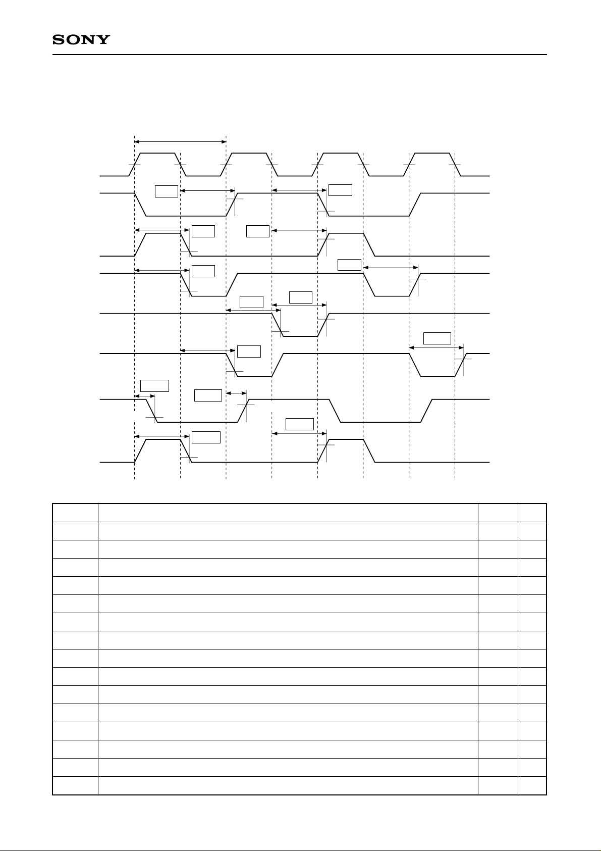
Waveform Characteristics of XH1 and RG
0.9V
DD
XH1
0.1VDD
CXD2424R
Symbol
trH1
tfH1
trRG
tfRG
RG
XH1 rise time
XH1 fall time
RG rise time
RG fall time
0.9VDD
0.1VDD
tfH1
trRG
tfRG
trH1
(VDD = 5.0V, Topr = 25°C, Load capacity of XH1 = 10pF, Load capacity of RG = 10pF)
Definition Typ. Unit
2
3
2
2
ns
ns
ns
ns
– 8 –
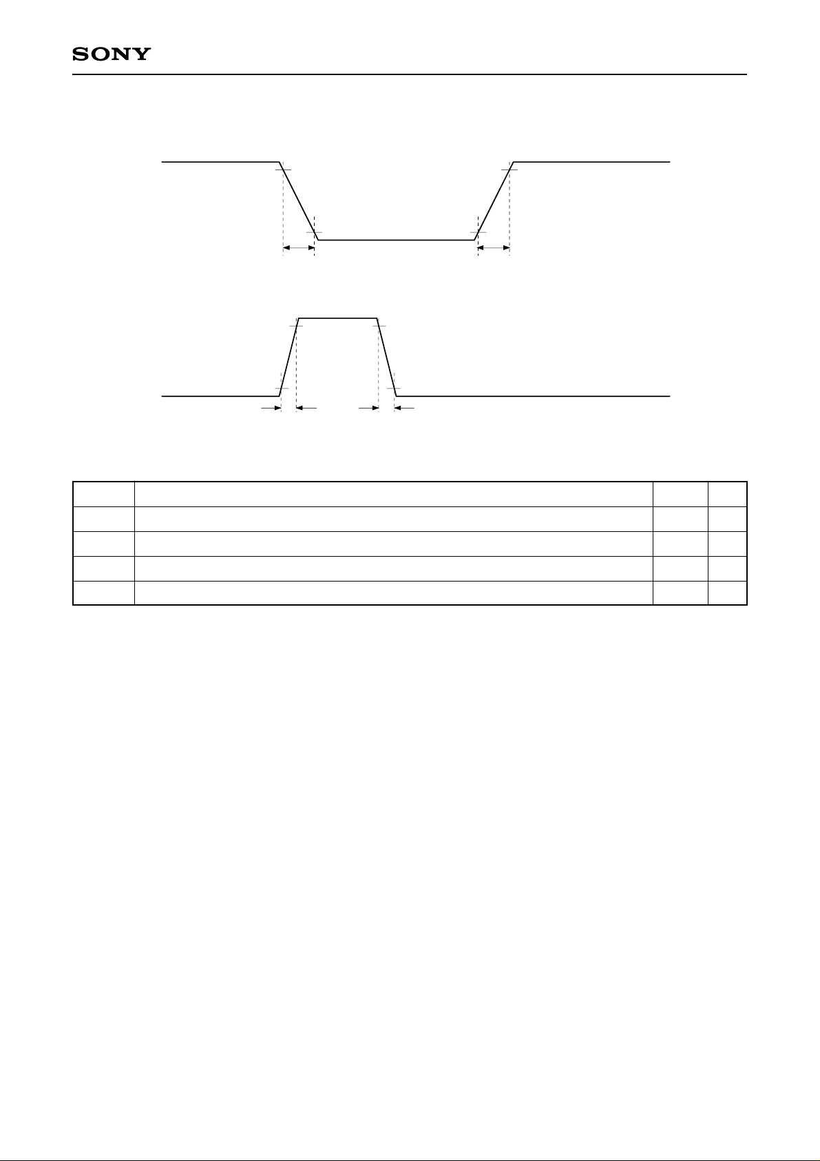
CXD2424R
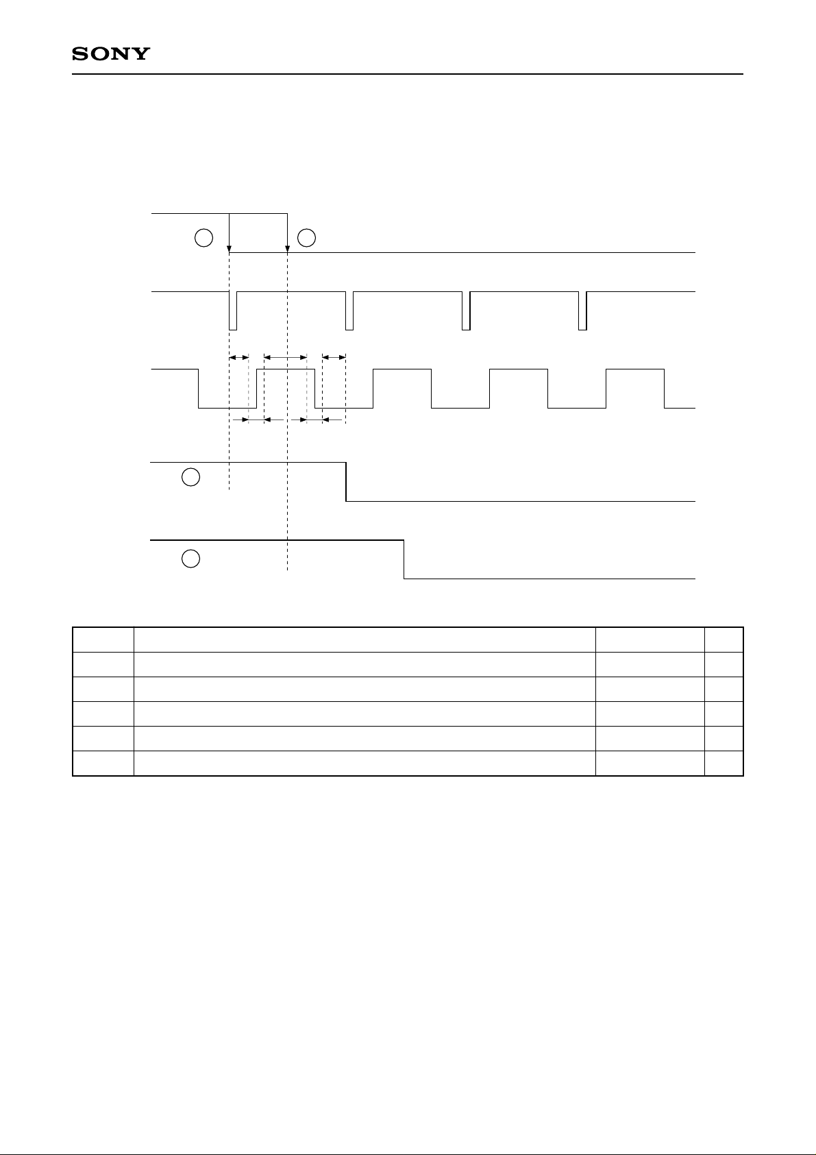
• In the normal reset mode, the signal output is reset to ODD or EVEN field depending on the input timing of
the vertical reset signal as shown in the figure below.
Field identification
VRI
HDO
VDO
VDO
1
tp1
H
f
tp4
1
2
tp2
2
tp5
tp3
fH
309.5H
L: ODD H: EVEN
309.5H
ODD
EVEN
Symbol
tp1
tp2
tp3
tp4
tp5
Range of resetting to ODD
Range of resetting to EVEN
Range of resetting to ODD
Prohibited area
Prohibited area
Definition Specified value Unit
22.0
31.8
9.8
200
200
µs
µs
µs
ns
ns
– 9 –
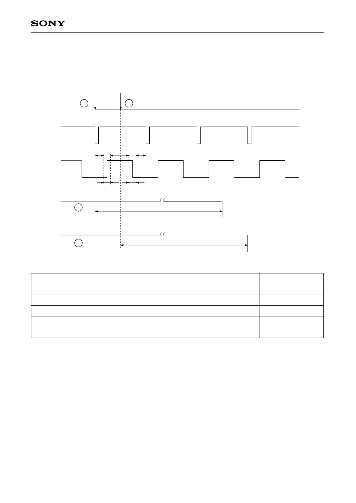
CXD2424R
• In the direct reset mode, the signal output is reset to ODD or EVEN field depending on the input timing of the
vertical reset signal as shown in the figure below.
Field identification
VRI
HDO
VDO
VDO
1
tp1
f
H
tp4
1
2
tp2
2
tp3
L: ODD H: EVEN
tp5
fH
EVEN
ODD
Symbol
tp1
tp2
tp3
tp4
tp5
∗1
In the direct reset mode, the cycle of HD can be arbitrary. Therefore, tp3 is not specified.
Range of resetting to ODD
Range of resetting to EVEN
∗1
Range of resetting to ODD
Prohibited area
Prohibited area
Definition Specified value Unit
22.0
31.8
—
200
200
µs
µs
µs
ns
ns
– 10 –
 Loading...