

Sony CXD2401R Datasheet
Description
The CXD2401R is an IC which performs electronic
iris control by applying a CCD electronic shutter.
Features
• Electronic iris control drive
• Generates system clocks in response to the
CXA1390AR series
• Generates timing pulses to drive the 510H system
CCD image sensor
•
H driver for CCD (5V direct drive for Type 1/3 CCD)
Absolute Maximum Ratings
• Supply voltage VDD VSS – 0.5 to +7.0 V
• Input voltage VI VSS – 0.5 to VDD + 0.5V
• Output voltage VO VSS – 0.5 to VDD + 0.5V
•
Operating temperature
Topr –20 to +75 °C
• Storage temperature Tstg –55 to +150 °C
Recommended Operating Conditions
• Supply voltage VDD 4.75 to 5.25 V
•
Operating temperature
Topr –20 to +75 °C
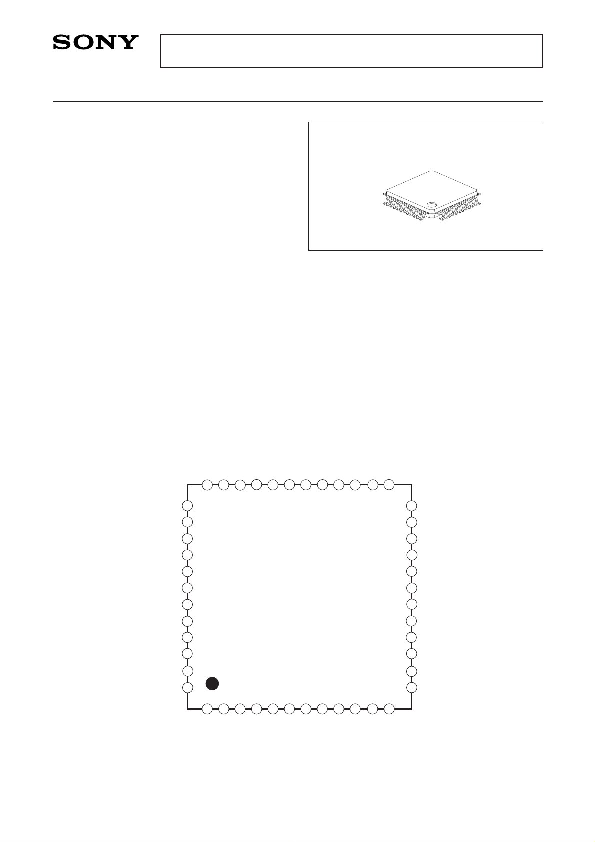
Pin Configuration
Applications
CCD monitoring cameras
Structure
Silicon gate CMOS IC
Applicable CCD Image Sensors
510H system SONY CCD
• ICX054BK (Type 1/3 NTSC CCD)
• ICX055BK (Type 1/3 PAL CCD)
– 1 –
CXD2401R
E94620D9X
Electronic Iris Control IC
Sony reserves the right to change products and specifications without prior notice. This information does not convey any license by
any implication or otherwise under any patents or other right. Application circuits shown, if any, are typical examples illustrating the
operation of the devices. Sony cannot assume responsibility for any problems arising out of the use of these circuits.
48 pin LQFP (Plastic)
2
3
4
5
6
7
8
9
10
11
12
13
14
15
16
17
18
19
20
21
22
23
24
25
26
27
28
29
30
40
39
38
37
36
35
34
31
32
33
41
42
43
44
45
46
47
48
1
CXD2401R
XV2
XDL2
XDL1
XSP2
XSP1
XSHP
V
SS2
XSHD
V
DD2
CLP2
BFG
ID
V
SS4
SPUPV
IRIN
SPDNV
Vreg
V
DD4
ENB
IRENB
PS
LIMIT1
LIMIT2
NTSC
GM
V
DD
3
RG
H2
H1
V
SS
3
XSUB
XV4
XSG2
XV3
XSG1
XV1
OSCI
OSCO
CK
TEST
CL
V
SS
1
VD
HD
V
DD
1
CLP4
CLP1
PBLK

– 2 –
CXD2401R
Pin Description
Pin
No.
1
2
3
4
5
6
7
8
9
10
11
12
13
14
15
16
17
18
19
20
21
22
23
24
25
26
27
28
29
30
31
32
33
34
OSCI
OSCO
CK
TEST
CL
VSS1
VD
HD
VDD1
CLP4
CLP1
PBLK
ID
BFG
CLP2
VDD2
XSHD
VSS2
XSHP
XSP1
XSP2
XDL1
XDL2
XV2
XV1
XSG1
XV3
XSG2
XV4
XSUB
VSS3
H1
H2
RG
I
O
I
I
O
—
I
I
—
O
O
O
O
O
O
—
O
—
O
O
O
O
O
O
O
O
O
O
O
O
—
O
O
O
Inverter input for oscillation. (NTSC: 1820fH, PAL: 1816fH)
Inverter output for oscillation. (NTSC: 1820fH, PAL: 1816fH)
Input for main clock in IC. (NTSC: 1820fH, PAL: 1816fH)
IC test input. Fixed at GND in normal operation. (With pull-down resistor)
CK/2 clock output. NTSC: 910fH = 4fsc, PAL: 908fH
GND
Vertical sync signal input.
Horizontal sync signal input.
5V power supply.
Clamping pulse for CCD dummy output.
Clamping pulse for CCD optical black.
Cleaning pulse for vertical/horizontal blanking.
Vertical direction line identification signal.
Burst flag gate pulse.
Clamping pulse in horizontal blanking.
5V power supply.
CCD data level sample-and-hold pulse output.
GND
CCD precharge level sample-and-hold pulse output.
Color separation sample-and-hold pulse output.
Color separation sample-and-hold pulse output.
Clock output for CCD DL (Delay Line).
Clock output for CCD DL (Delay Line).
CCD vertical clock output.
CCD vertical clock output.
Clock output for CCD sensor readout.
CCD vertical clock output.
Clock output for CCD sensor readout.
CCD vertical clock output.
Clock output for CCD electronic shutter.
GND
CCD horizontal clock output.
CCD horizontal clock output.
CCD reset gate pulse output.
Symbol I/O Description
– 3 –
CXD2401R
Pin
No.
35
36
37
38
39
40
41
42
43
44
45
46
47
48
VDD3
GM
VSS4
SPUPV
IRIN
SPDNV
Vreg
VDD4
ENB
IRENB
PS
LIMIT1
LIMIT2
NTSC
—
I
—
I
I
I
—
—
I
I
I
I
I
I
5V power supply.
Used for GND connection.
GND
When set in electronic iris mode: Shutter speedup reference voltage input
When set in serial mode of electronic shutter: Strobe input
When set in electronic iris mode: Iris signal input
When set in serial mode of electronic shutter: Clock input
When set in electronic iris mode: Shutter speed-down reference voltage input
When set in serial mode of electronic shutter: Data input
Current source for comparator. Connected to 5V power supply via 33kΩ resistor.
5V power supply.
Generation/halt switching of electronic shutter pulse (Pin 30). (With pull-up resistor)
Electronic iris/electronic shutter switching. (With pull-up resistor)
Parallel/serial input switching of electronic shutter speed data. (With pull-up resistor)
Selecting limit value of max. shutter speed. (With pull-down resistor)
Selecting limit value of max. shutter speed. (With pull-down resistor)
NTSC/PAL switching. (With pull-down resistor)
Symbol I/O Description
Electrical Characteristics
DC Characteristics (Within recommended operating range)
Item
Supply voltage 1
Input voltage 1
Input voltage 2
Input voltage 3
∗
Output voltage 1
Output voltage 2
Output voltage 3
Output voltage 4
Pull-up
resistance value
Pull-down
resistance value
9, 16, 35, 42
38, 40 (Electronic iris mode)
39 (Electronic iris mode)
4, 7, 8, 36, 38, 39, 40, 43,
44, 45, 46, 47, 48 (Pins 38,
39 and 40 are when set in
electronic shutter mode)
5, 10, 11
15, 17, 19, 20, 21,
22, 23, 34
32, 33
12, 13, 14, 24, 25,
26, 27, 28, 29, 30
43, 44, 45
4, 36, 46, 47, 48
VDD
VIN1
VIN2
VIH3
VIL3
VOH1
VOL1
VOH2
VOL2
VOH3
VOL3
VOH4
VOL4
RPU
RPD
4.75
1.9
VSS
0.7VDD
VDD – 0.8
VDD – 0.8
VDD – 0.8
VDD – 0.8
25
25
5.0
50
50
5.25
VDD
VDD
0.3VDD
0.4
0.4
0.4
0.4
75
75
V
V
V
V
V
V
V
V
V
V
V
V
V
kΩ
kΩ
IOH = –4mA
IOL = 8mA
IOH = –8mA
IOL = 8mA
IOH = –20mA
IOL = 20mA
IOH = –2mA
IOL = 4mA
VIL = 0V
VIH = VDD
Pin No. Symbol Conditions Min. Typ. Max. Unit
∗
Pins 7 and 8 do not have a protective diode at the power supply side.
– 4 –
CXD2401R
Comparator Characteristics
Item
Input offset voltage
Response
time
Current consumption
In-phase input voltage range
Indefinite region
38, 39,
40
Vos
tpd+
tpd–
IDD
VICR
Vf
1.1
140
190
98
1.9 to 5
50
140
±10
mV
ns
ns
µA
V
mW
Response time when a step
input of 100mV amplitude/
5mV overdrive is applied.
Pin No. Symbol Conditions Min. Typ. Max. Unit
Rise
Fall
Bias current source for comparator. Pin No.: 41. Connected to power supply via 33kΩ resistor.
Oscillating Inverter I/O Characteristics
(Within recommended operating range)
(Within recommended operating range)
Item
Logical Vth
Input voltage
Output voltage
Feedback resistor
Oscillator frequency
1
2
1 to 2
LVth
VIH
VIL
VOH
VOL
RFE
f
0.7VDD
VDD/2
250k
20
VDD/2
1M
0.3VDD
VDD/2
2.5M
30
V
V
V
V
V
Ω
MHz
IOH = –12mA
IOL = 12mA
VIN = VDD or Vss
Pin No. Symbol Conditions Min. Typ. Max. Unit
Duty Control Inverter Input Characteristics (Within recommended operating range)
Item
Logical Vth
Input voltage
Input amplification
Feedback resistor
3
LVth
VIH
VIL
VIN
RFE
0.7VDD
0.5
250k
VDD/2
1M
0.3VDD
2.5M
V
V
V
Vpp
Ω
fmax = 50MHz sine wave
VIN = VDD or Vss
Pin No. Symbol Conditions Min. Typ. Max. Unit
Note) The input voltage is the input voltage characteristics for an external direct power input, and input
amplification is the input amplification characteristics for input through capacitor.
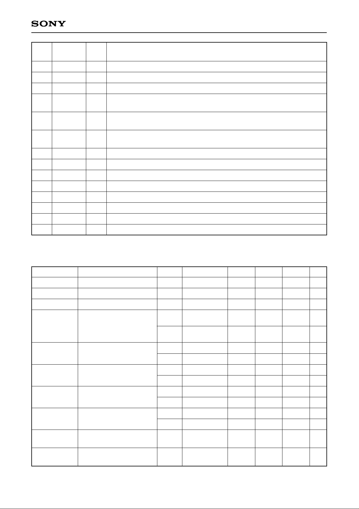
Note) 1. Input offset voltage and indefinite region
Input offset voltage and indefintie region are
existed in the comparator which builds in this IC
as shown right figure. Note that this when
designing external circuit.
2. Pins 40 and 38 for electronic iris mode
Use it in this state of Pin 40 (SPDNV) > Pin 38
(SPUPV).
10mV
10mV
10mV
10mV
Input offset voltage
Input offset voltage
50mV
50mV
5.0V
GND
Indefinite region
Indefinite region
Pins 40 and 38
(SPDNV and SPUPV)
– 5 –
CXD2401R
Electrical Characteristics
AC Characteristics
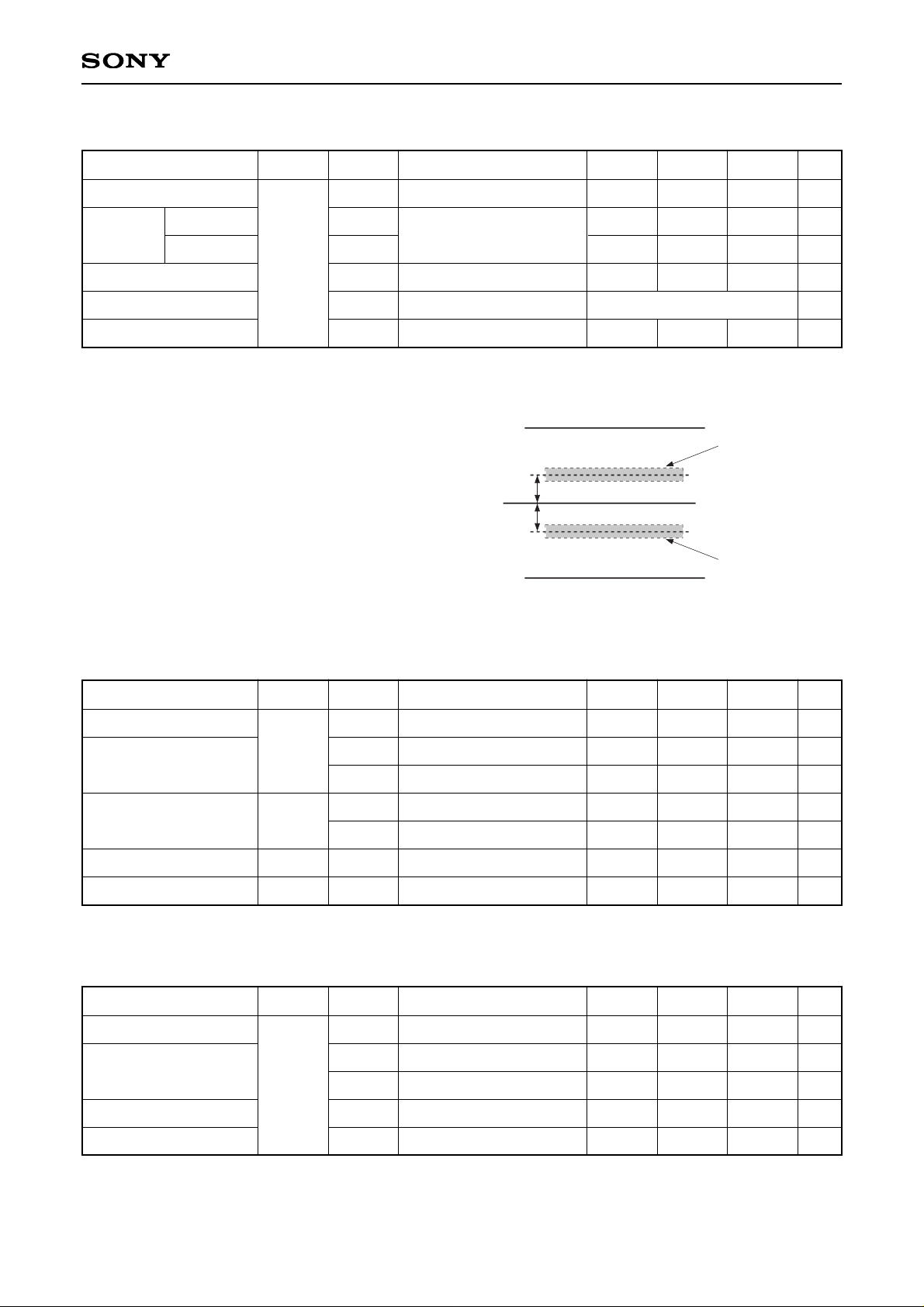
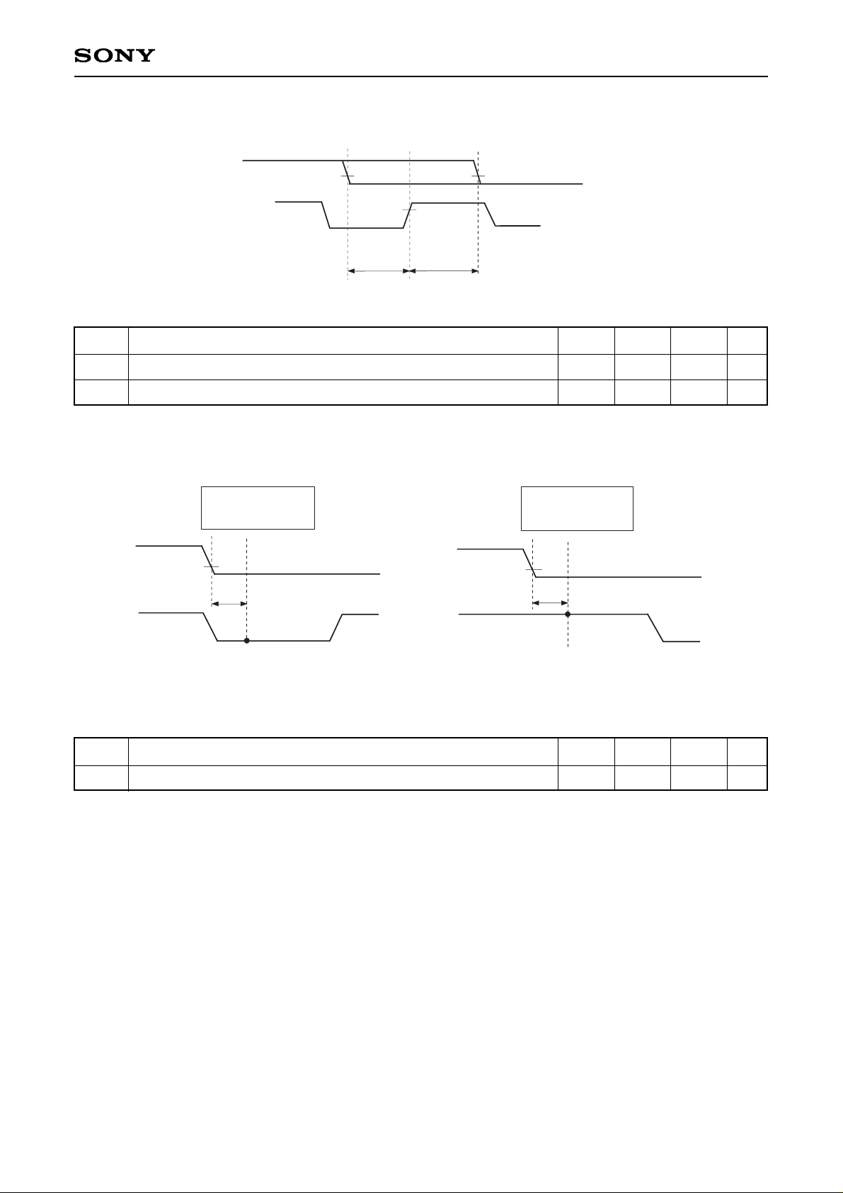
1) AC characteristics among serial communication clocks (SPDNV (ED2), IRIN (ED1), SPUPV (ED0))
ts2
th2
SPDNV (ED2)
IRIN (ED1)
SPUPV (ED0)
ts1
ts0
tw0
0.3V
DD
0.7VDD
0.7VDD
0.7VDD
0.7VDD
0.3VDD
(Within recommended operating range)
Symbol
ts2
th2
ts1
tw0
ts0
SPDNV (ED2) set-up time, activated by the rising edge of IRIN (ED1)
SPDNV (ED2) hold time, activated by the rising edge of IRIN (ED1)
IRIN (ED1) rising set-up time, activated by the rising edge of SPUPV
(ED0)
SPUPV (ED0) pulse width
SPUPV (ED0) rising set-up time, activated by the rising edge of IRIN
(ED1)
20ns
20ns
20ns
20ns
20ns
50µs
Definition Min. Typ. Max.
2) Microcomputer communication clock → IC take-in characteristics
VD
HD
XSG1
HD
XSG1
0.3VDD 0.3VDD
Example: NTSC/ODD field
Magnification
SEN logic level is to be High for this period.
NTSC mode: 63.5µs, PAL mode: 63.9µs
Note) During the 1H period for generating XSG1, the phase against AVD differs according to each mode.
Please always maintain the SEN logic level at High for "the 1H period when XSG1 varies."
– 6 –
CXD2401R
3) HD/VD take-in characteristics
HD
VD
CL
ts4
th4
0.7V
DD
0.3VDD 0.3VDD
4) Phase discrimination characteristics by VD/HD input
VD
HD
VD
HD
tpd2
tpd2
0.3VDD
0.3VDD
NTSC: ODD field
NTSC: EVEN field
When the HD logic level is Low tpd2 after VD falls,
the phase is discriminated as an ODD field (NTSC).
When the HD logic level is High tpd2 after VD falls,
the phase is discriminated as an EVEN field (NTSC).
PAL: EVEN field
PAL: ODD field
(Within recommended operating range, Load capacity of CL = 30pF)
Symbol
ts4
th4
HD/VD set-up time, activated by CL
HD/VD hold time, activated by CL
5
7
ns
ns
Definition Min. Typ. Max. Unit
(Within recommended operating range)
Symbol
tpd2
Field discriminating clock phase, activated by the falling edge of VD 700
1000
ns
Definition Min. Typ. Max. Unit

– 7 –
CXD2401R
5) Phase characteristics of H1, RG, XSHP, XSHD, XSP1, XSP2, XDL1, XDL2, and CL
tCK
H1
0.3V
DD
tpd4
tpd5
RG
tpd6
XSHP
tpd7
tpd8
tpd9
tpd10
XSHD
CL
XSP2
XDL1
XDL2
0.3VDD
0.7VDD
0.7VDD
0.7VDD
0.3VDD
tpd11
tpd12
tpd13
tpd14
tpd16
tpd17
0.3VDD
CK
Vpp/2
tpd3
0.7VDD
0.3VDD
0.7VDD
0.3VDD
0.7VDD
0.3VDD
XSP1
0.3VDD
0.7VDD
0.3VDD
0.7VDD
0.7VDD
tpd18
tpd20
tpd19
tpd15
(Within recommended operating range)
CK-duty = within 50 ± 4%, Load capacity of H1 = 150pF, Load capacity of CL = 30pF, Load capacity of RG,
XSHP, XSHD, XSP1, XSP2, XDL1, and XDL2 = 10pF
Symbol
tCK
tpd3
tpd4
tpd5
tpd6
tpd7
tpd8
tpd9
tpd10
tpd11
tpd12
tpd13
tpd14
tpd15
tpd16
tpd17
tpd18
tpd19
tpd20
CK cycle
H1 falling delay, activated by the falling edge of CK
H1 rising delay, activated by the rising edge of CK
RG falling delay, activated by the falling edge of CK
RG rising delay, activated by the rising edge of CK
XSHP falling delay, activated by the rising edge of CK
XSHP rising delay, activated by the falling edge of CK
XSHD falling delay, activated by the falling edge of CK
XSHD rising delay, activated by the rising edge of CK
XSP1 falling delay, activated by the rising edge of CK
XSP1 rising delay, activated by the rising edge of CK
XSP2 falling delay, activated by the rising edge of CK
XSP2 rising delay, activated by the rising edge of CK
XDL1 rising delay, activated by the rising edge of CK
XDL1 falling delay, activated by the falling edge of CK
XDL2 rising delay, activated by the rising edge of CK
XDL2 falling delay, activated by the falling edge of CK
CL falling delay, activated by the falling edge of CK
CL rising delay, activated by the falling edge of CK
16.22
17.25
20.18
18.61
15.86
15.76
14.92
14.76
14.79
15.05
15.09
15.29
14.49
15.05
14.46
14.92
15.33
14.71
35
29
31
36
33
28
28
27
26
26
27
27
27
26
27
26
27
27
26
56.9
60.38
70.58
65.32
55.59
55.32
52.26
51.62
51.74
52.58
52.82
53.54
50.79
52.67
50.65
52.47
53.01
51.58
ns
ns
ns
ns
ns
ns
ns
ns
ns
ns
ns
ns
ns
ns
ns
ns
ns
ns
ns
Definition Min. Typ. Max. Unit
 Loading...