

Sony CXD2400R Datasheet

Timing Controller for CCD cameras
Description
The CXD2400R is a timing controller for CCD
camera systems which use the ICX044/045,
ICX054/055 or other black/white CCD image
sensors.
Features
• Supports EIA/CCIR standards
• Electronic iris (electronic shutter) function
• Sync signal generation function
• Supports external synchronization
• Supports non-interlacing
• Supports field/frame∗accumulation
• Oscillator frequency: 1212 fh
(EIA: 19.0699MHz; CCIR: 18.9375MHz)
∗
The characteristics of CCD image sensors are
guaranteed for field accumulation operation.
CXD2400R
48 pin LQFP (Plastic)
Applications
CCD cameras
Structure
Silicon gate CMOS IC
Absolute Maximum Ratings (Ta = 25°C)
• Supply voltage VDD Vss – 0.5 to +7.5 V
• Input voltage VI
• Output voltage Vo
•
Operating temperature
•
Storage temperature
Recommended Operating Conditions
• Supply voltage 5.0V ± 0.25 V
•
Operating temperature
Topr –20 to +75 °C
Tstg –55 to +150 °C
Vss – 0.5 to VDD + 0.5
Vss – 0.5 to VDD + 0.5
–20 to +75 °C
V
V
Sony reserves the right to change products and specifications without prior notice. This information does not convey any license by
any implication or otherwise under any patents or other right. Application circuits shown, if any, are typical examples illustrating the
operation of the devices. Sony cannot assume responsibility for any problems arising out of the use of these circuits.
– 1 –
E93308D75-PS
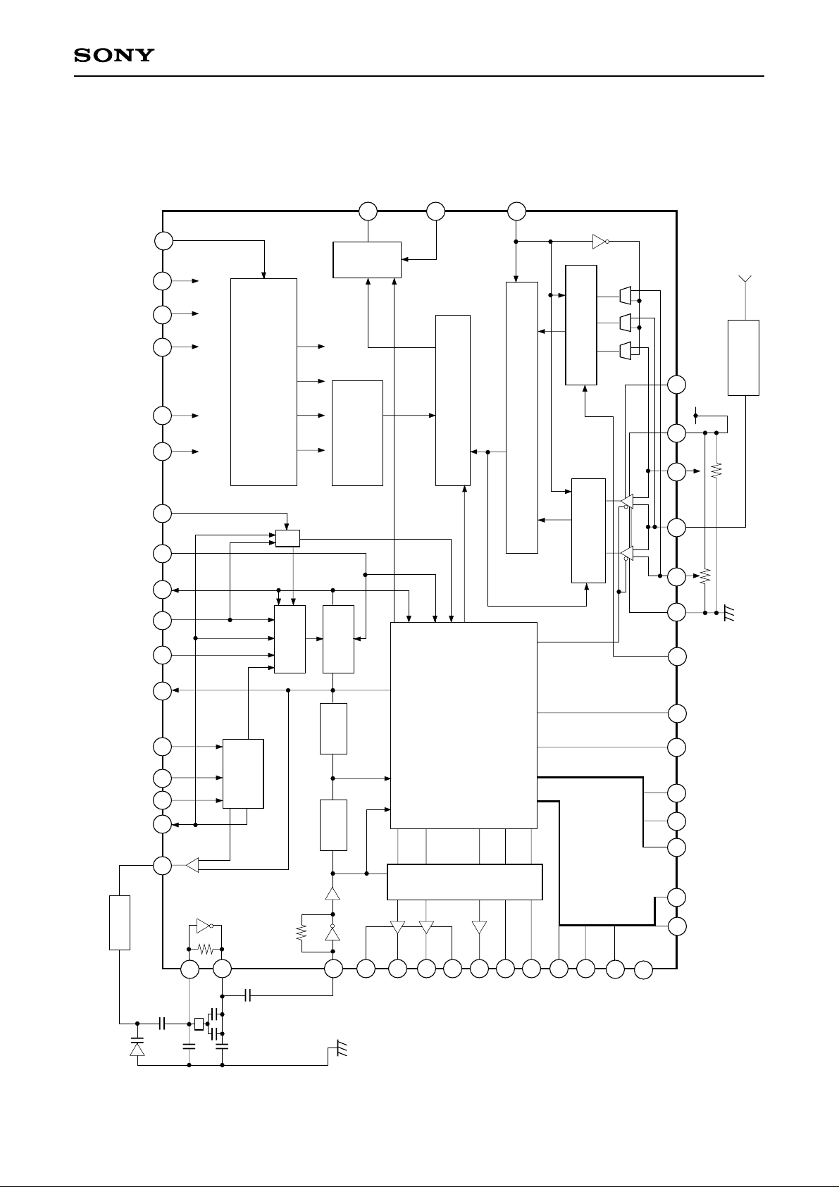
CXD2400R
DD1VDD2 Vss1 Vss2 Vss3 TEST
LSEL VDNIL EIA FL/FR V
44
31
18
6
43
19
28
27
33
41
42
TEST CIRCUIT
Field/
O/E
GEN
RESET
XSUB
13
GATE
CK GEN
IRIS/SHUTTER
Frame
1/525
1/625
ENB
14
CK
COUNTER
D
IRENB
15
SELECTOR
DECODE
ED0 ED1 ED2
P/S
UP/DOWN ADDER
20
CVDD
21
23
17
22
24
16
Vreg
/ED0
SPUPV
IRIN
/ED1
/ED2
SPDNV
CVss
VIDEO SIG.
LPF
HD
34
39
38
HPLLVR/SYNC
40
ESYNC
37
EXT
HCOMP
45
LPF
Block Diagram
LCIN
46
L
47
LCOUT
VR1HD1
SEP
SYNC
12 12fH
1/606
1/2
48
CKI
4
SS
AV
2
H1
3
H2
TG/SSG
GATE
1
DD
AV
5
RG
25
SHP
26
SHD
8
XV1
7
XV2
10
XV3
12
XV4
29
30
32
36
35
11
9
CLP1 CLP2 PS
CBLK
XSG1 XSG2 SYNC FLD
– 2 –
CXD2400R
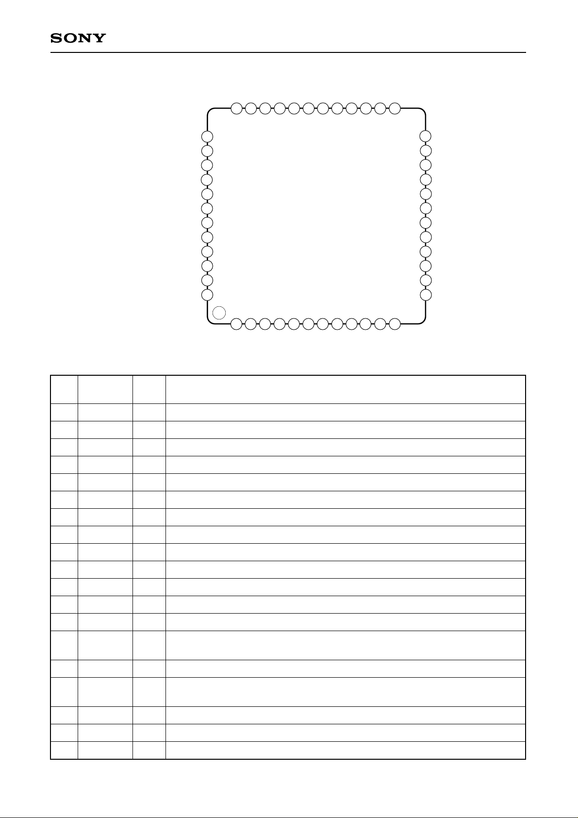
Pin Configuration (Top View)
VR/SYNC
ESYNC
HCOMP
LCOUT
Pin Description
EXT
HPLL
NIL
LSEL
DD2
V
TEST
LCIN
CKI
38
39
40
41
42
43
44
45
46
47
48
37
36
CBLK
35
DD
AV
SYNC
2
H1
34
3
SS
CLP2
32
5
FLD
RG
31
V
CLP1
FL/FR
7
XV2
29
8
XV1
28
9
10
XSG1
30
6
1
SS
V
HD
VD
33
4
3
SS
H2
AV
EIA
XV3
2627
11
SHD
25
121
XSG2
SHP
XV4
CV
24
23
SPUPV/ED0
22
SPDNV/ED2
CV
21
20
Vreg
19
VDD1
18
V
17
IRIN/ED1
16
PS
15
IRENB
14
ENB
13
XSUB
SS
DD
SS2
Pin
No.
1
2
3
4
5
6
7
8
9
10
11
12
13
14
Symbol I/O Description
AVDD
H1
H2
AVss
RG
Vss1
XV2
XV1
XSG1
XV3
XSG2
XV4
XSUB
ENB
—
Power supply (for H1, H2)
∗2
O
O
O
H1 clock output for CCD horizontal register drive
∗2
H2 clock output for CCD horizontal register drive
—
GND (for H1, H2)
∗5
Reset gate pulse output
—
GND
O
XV2 clock output for CCD vertical register drive
O
XV1 clock output for CCD vertical register drive
O
CCD sensor charge readout pulse output
O
XV3 clock output for CCD vertical register drive
O
CCD sensor charge readout pulse output
O
XV4 clock output for CCD vertical register drive
O
CCD discharge pulse output
XSUB pulse output ON/OFF control (with pull-up resistance)
I
Low: XSUB pulse output stop; high: XSUB pulse output
15
16
17
18
19
IRENB
PS
IRIN/ED1
Vss2
VDD1
I
Low: Electronic shutter mode; high: electronic iris mode (with pull-up resistance)
Electronic shutter speed input switchover (with pull-up resistance)
I
Low: Serial input; high: parallel input
∗1
I
Iris signal input/shutter speed setting; clock input in serial mode.
—
GND
—
Power supply
– 3 –
CXD2400R
Pin
No.
20
21
22
23
24
25
26
27
28
29
30
31
32
Symbol I/O Description
Vreg
CVDD
SPDNV
/ED2
SPUPV
/ED0
CVss
SHP
SHD
EIA
FL/FR
CLP2
CLP1
Vss3
FLD
—
Bias current supply for comparator
—
Power supply (for comparator)
Shutter speed down reference voltage/
∗1
I
Shutter speed setting; data input in serial mode
Shutter speed up reference voltage/
∗1
I
Shutter speed setting; strobe input in serial mode
—
GND (for comparator)
∗1
O
O
Precharge level sample-and-hold pulse
∗1
Data sample-and-hold pulse
I
Low: EIA; high: CCIR (with pull-down resistance)
Field accumulation/frame accumulation, odd field/even field switchover
I
(with pull-down resistance)
O
Pulse output for clamp
O
Pulse output for clamp
—
GND
O
Field identification signal output High: odd field; low: even field
33
VD
34
HD
35
SYNC
36
CBLK
37
EXT
38
HPLL
39
VR/SYNC
40
ESYNC
41
NIL
42
LSEL
43
VDD2
44
TEST
45
HCOMP
46
LCIN
47
LCOUT
48
CKI
∗1
O
→ POWERED BUFFER
∗2
O
→ Hdriver Cell
∗3
O
→ OSCILLATOR Cell
∗4
O
→ Phase Comparater
∗5
O
→ RGdriver Cell
O
Vertical drive output
O
Horizontal drive output
O
Composite sync output
O
Composite blanking output
O
External sync/internal sync identification signal High: external sync; Low: internal sync
I
Horizontal drive signal input (with pull-up resistance)
I
Vertical drive signal input/composite sync input (with pull-up resistance)
I
Low: SYNC sync or internal sync; high: VD/HD sync (with pull-down resistance)
I
Low: interlace mode; high: non-interlace mode (with pull-down resistance)
Line number selection pin (with pull-down resistance)
I
Low: EIA 262H/CCIR 312H; high: EIA 263H/CCIR 313H
—
Power supply
I
Fixed to low level (with pull-down resistance)
∗4
O
O
H comparator output
∗2
I
LC oscillation (crystal oscillator) inverter input
∗3
LC oscillation (crystal oscillator) inverter output
∗3
I
Clock input
∗1
I
→ Comparater Input
∗2
I
→ OSCILLATOR Cell
∗3
I
→ Input cell with feedback resistance
– 4 –
CXD2400R
Electrical Characteristics
1) DC Characteristics (VDD = 5V ± 0.25V, Topr = –20 to +75°C)
Item
Supply voltage
Input voltage 1
(All input pins except those below)
Input voltage 2
(Pins 22, 23 only in electronic
iris mode)
Input voltage 3
(Pin 17 only in electronic
iris mode)
Output voltage 1
(All output pins except those below)
Output voltage 2
(Pins 25, 26)
Output voltage 3
(Pin 5)
Output voltage 4
(Pins 2, 3)
Symbol Conditions Min. Typ. Max. Unit
VDD
VIH1
VIL1
VIN2
VIN3
VOH1
VOL1
VOH2
VOL2
VOH3
VOL3
VOH4
VOL4
IOH = –2mA
IOL = 4mA
IOH = –4mA
IOL = 8mA
IOH = –8mA
IOL = 8mA
ICH = –20mA
ICL = 20mA
4.75
0.7VDD
2.0
VSS
VDD – 0.8
VDD – 0.8
VDD – 0.8
VDD – 0.8
5.0
5.25
0.3VDD
VDD
VDD
0.4
0.4
0.4
0.4
V
V
V
V
V
V
V
V
V
V
V
V
V
Output voltage 5
(Pin 47)
Output voltage 6
(Pin 45)
Feedback resistance
Pull-up resistance
Pull-down resistance
VOH5
VOL5
VOH6
VOL6
RFB
RPU
RPD
IOH = –3mA
IOL = 3mA
IOH = –4mA
IOL = 4mA
VIN = Vss or VDD
VIL = 0V
VIH = VDD
VDD/2
VDD – 0.8
250k
25k
25k
VDD = 5V
Current consumption
IDD
ICX054AL in normal
operating state
∗
Power consumption: 180mW typ., ICX054AL load (in normal operating state)
2) Input/output capacitance (VDD = V1 = 0V, fM = 1MHz)
Item
Input pin capacitance
Output pin capacitance
Input/output pin capacitance
Symbol
CIN
COUT
CI/O
Min. Typ. Max. Unit
9
11
11
pF
pF
pF
1M
50k
50k
36
VDD/2
0.4
2.5M
75k
75k
V
V
V
V
Ω
Ω
Ω
mA
– 5 –
3) Comparator characteristics (VDD = 5V ± 0.25V, Topr = –20 to +75°C)
CXD2400R
Item
Input offest voltage
Indefinite region
Symbol
VOS
Vf
Min. Typ. Max. Unit
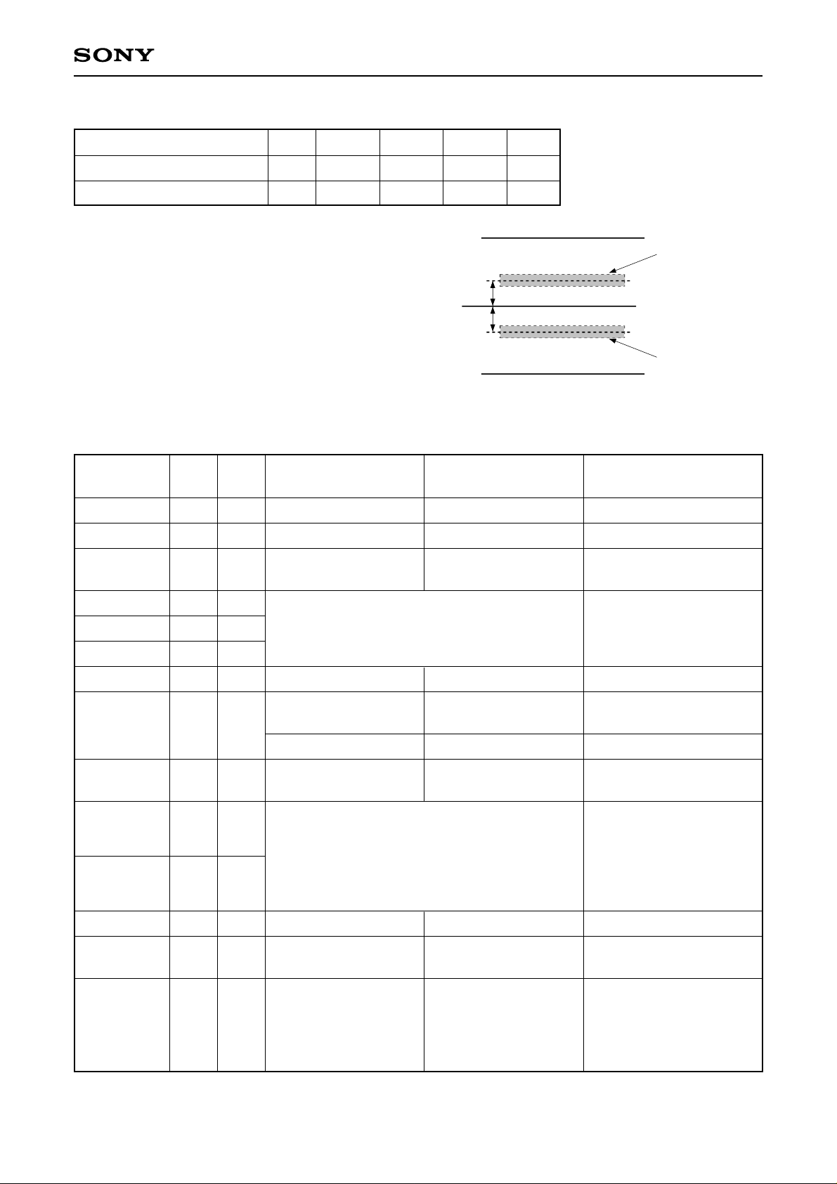
Note) 1. Input offset voltage and indefinite region
Input offset voltage and indefintie region are
existed in the comparator which builds in this IC
as shown right figure. Note that this when
designing external circuit.
2. Pins 22 and 23 for electronic iris mode
Use it in this state of Pin 22 (SPDNV) > Pin 23
(SPUPV).
Mode Control
Symbol
ENB
IRENB
Pin
No.
14
15
I/O Low High Remarks
I
I
XSUB stop
Electronic shutter
50
±10
5.0V
50mV
50mV
GND
Input offset voltage
Input offset voltage
XSUB output
Electronic iris
mV
mV
Indefinite region
10mV
10mV
Pins 22 and 23
(SPDNV and SPUPV)
10mV
10mV
Indefinite region
Valid only when ENB is high.
PS
IRIN/ED1
SPDNV/ED2
SPUPV/ED0
EIA
FL/FR
ESYNC
HPLL
VR/SYNC
NIL
LSEL
16
17
22
23
27
28
40
38
39
41
42
I
I
I
I
I
Serial input
Electronic iris control signal input pin
(IRENB = high)
Shutter speed setting pin
(IRENB = Low)
EIA
Odd field
I
Field accumulation
I
SYNC sync
Internal sync
Internal sync : HPLL (Open)
I
VR/SYNC (Open)
SYNC sync : HPLL (Open)
VR/SYNC (SYNC input)
VD/HD sync : HPLL (HD input)
I
VR/SYNC (VD input)
I
I
Interlace
EIA : 262H
CCIR : 312H
Parallel input
CCIR
Even field
Frame accumulation
VD/HD sync
Non-interlace
EIA : 263H
CCIR : 313H
Valid only when ENB is
high and IRENB is low.
Valid only when ENB is
high.
Valid only when NIL is high
and EXT is low.
∗
All other modes.
Valid only when EXT is low.
Valid only when EXT is low
and NIL is high.
Switchover between
internal and external sync
EXT
37
O
Internal sync
External sync
is autonatically identified
by input state at Pins 38,
39 and 40.
∗
The characteristics of CCD image sensors are quaranteed for field acccumulation operation.
– 6 –
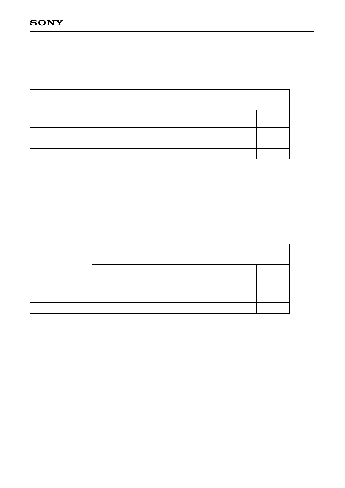
Mode Tables
CXD2400R
1) Internal sync mode HPLL pin (Pin 38)
VR/SYNC pin (Pin 39)
ESYNC pin (Pin 40)
Non-interlace
Interlace
Odd field
Field
readout
XSUB pulse OFF
Electronic shutter ON
Electronic iris ON
∗1
EIA for 1/60 s accumulation; CCIR for 1/50 s accumulation
∗2
Line number is 262H or 263H for EIA and 312H or 313H for CCIR.
∗3
The characteristics of CCD image sensors are guaranteed for field accumulation operation.
∗1
O
O
O
Frame
readout
O
O
O
∗3
Field
readout
O
O
O
∗2
Frame
readout
×
×
×
∗3
Even field
Field
readout
O
O
O
O: Can be used.
×: Cannot be used.
2) SYNC sync (external sync) mode HPLL pin (Pin 38)
VR/SYNC pin (Pin 39)
ESYNC pin (Pin 40)
: Open
: Open
: Open
∗2
Frame
readout
∗3
×
×
×
: Open
: SYNC input
: Open
Interlace
Odd field
Field
readout
XSUB pulse OFF
∗1
Electronic shutter ON
Electronic iris ON
∗1
EIA for 1/60 s accumulation; CCIR for 1/50 s accumulation
∗2
Line number is 262H or 263H for EIA and 312H or 313H for CCIR.
∗3
The characteristics of CCD image sensors are guaranteed for field accumulation operation.
O
O
O
Frame
readout
O
O
O
∗3
Field
readout
×
×
×
∗2
Frame
readout
×
×
×
∗3
Even field
Field
readout
×
×
×
O: Can be used.
×: Cannot be used.
Non-interlace
∗2
Frame
readout
×
×
×
∗3
– 7 –
 Loading...