

Sony CXD2309Q Datasheet

—1—
E94341B01
Sony reserves the right to change products and specifications without prior notice. This information does not convey any license by
any implication or otherwise under any patents or other right. Application circuits shown, if any, are typical examples illustrating the
operation of the devices. Sony cannot assume responsibility for any problems arising out of the use of these circuits.
Absolute Maximum Ratings (Ta=25 °C)
• Supply voltage AVDD, DVDD 7V
•Input voltage (All pins)
VIN VDD+0.5 to VSS–0.5 V
• Output current IOUT 0 to 15 mA
• Storage temperature
Tstg –55 to +150 °C
Recommended Operating Conditions
• Supply voltage AVDD, AVSS 4.75 to 5.25 V
DVDD, DVSS 4.75 to 5.25 V
• Reference input voltage
VREF 0.5 to 2.0 V
• Clock pulse width
TPW1, TPW0 9 (min.) ns
• Operating temperature
Topr –20 to +85 °C
Description
The CXD2309Q is a 10-bit high-speed D/A
converter for video band, featuring RGB 3-channel
input/output. This is ideal for use in high-definition
TVs and high-resolution displays.
Features
• Resolution 10-bit
• Maximum conversion speed 85MSPS
• RGB 3-channel input/output
• Differential linearity error ±0.5 LSB
• Low power consumption 275 mW
(200 Ω load for 2 Vp-p output)
• Single +5 V power supply
• Low glitch
• 48-pin QFP package
Structure
Silicon gate CMOS IC
10-bit 85MSPS 3-Channel D/A Converter
48 pin QFP (Plastic)
CXD2309Q
—2—
CXD2309Q
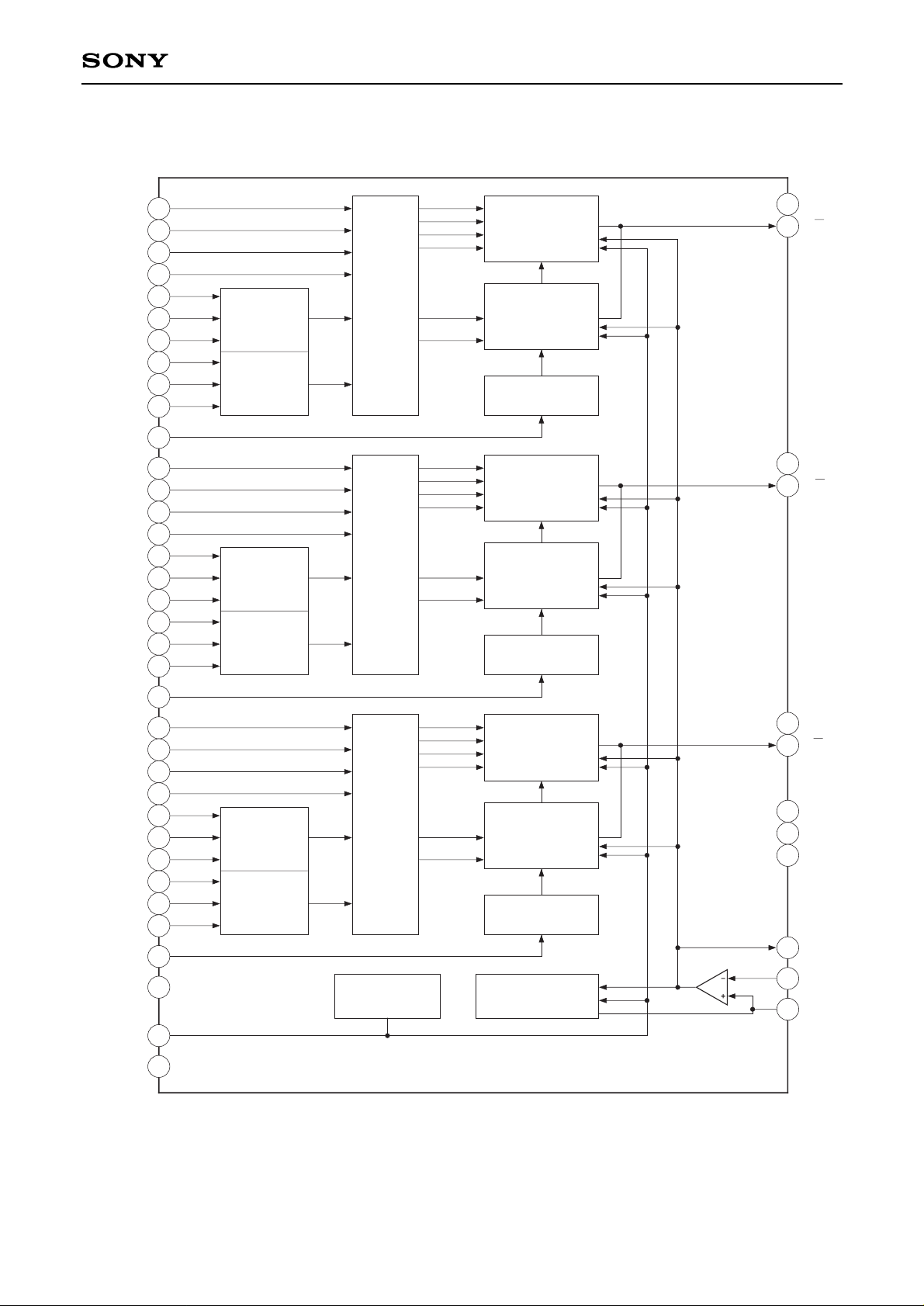
Block Diagram
DECODER
DECODER
LATCHES
4LSB’S
CURRENT
CELLS
DECODER
DECODER
LATCHES
6LSB’S
CURRENT
CELLS
CLOCK
GENERATOR
4LSB’S
CURRENT
CELLS
6LSB’S
CURRENT
CELLS
CLOCK
GENERATOR
DECODER
DECODER
LATCHES
4LSB’S
CURRENT
CELLS
6LSB’S
CURRENT
CELLS
CLOCK
GENERATOR
1
2
3
4
5
6
7
8
9
10
11
12
13
14
15
16
17
18
19
20
31
32
33
48
21
22
23
24
25
26
27
28
29
30
35
34
CURRENT CELLS
(FOR FULL SCALE)
BIAS VOLTAGE
GENERATOR
43
42
44
45
46
47
41
40
39
38
37
36
(LSB) R0
R1
R2
R3
R4
R5
R6
R7
R8
(MSB) R9
RCK
(LSB) G0
G1
G2
G3
G4
G5
G6
G7
G8
(MSB) G9
GCK
(LSB) B0
B1
B2
B3
B4
B5
B6
B7
B8
(MSB) B9
BCK
DV
DD
VB
DV
SS
AVSS
RO
AV
SS
GO
AV
SS
BO
AV
DD
AVDD
AVDD
VG
VREF
IREF
—3—
CXD2309Q
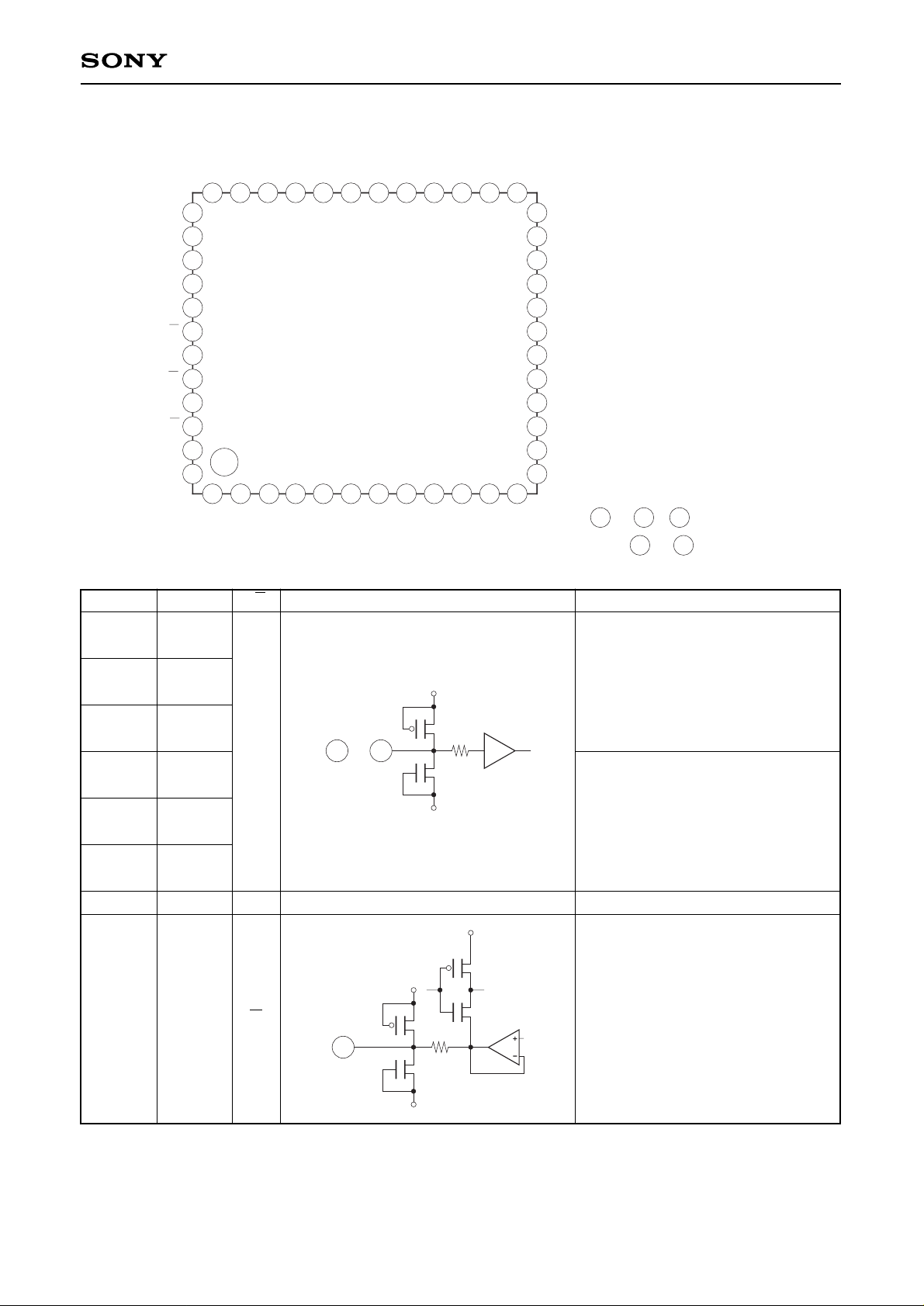
Pin Configuration
2 31 4 5 6 7 8 9
10 11 12
22
23
24
21
20
19
18
17
16
15
14
13
35 34 33 32 31 30 29 28 27 26 2536
46
45
44
43
42
41
40
39
38
47
48
37
(LSB) R0
R1
R2
R3
R4
R5
R6
R7
R8
(MSB) R9
(LSB) G0
G1
IREF
VB
DV
SS
BCK
GCK
RCK
B9 (MSB)
B8
B7
B6
B5
B4
B3
B2
B1
B0 (LSB)
G9 (MSB)
G8
G7
G6
G5
G4
G3
G2
1
35,48
36 47
to
to
Digital system
Analog system
VG
AV
DD
AVDD
AVDD
RO
AV
SS
GO
AV
SS
BO
AV
SS
DVDD
VREF
Pin Description and Equivalent Circuit
Pin No. Symbol I/O Equivalent circuit Description
1 to 10
11 to 20
21 to 30
31
32
33
34
35
R0 to R9
G0 to G9
B0 to B9
RCLK
GCLK
BCLK
DVSS
VB
I
—
O
DVDD
DVSS
33
1
to
Digital input.
1 pin R0 (LSB) to 10 pin R9 (MSB)
11 pin G0 (LSB) to 20 pin G9 (MSB)
21 pin B0 (LSB) to 30 pin B9 (MSB)
Clock input.
Digital ground.
Connect an approximately 0.1µF
capacitor.
DVDD
DVSS
35
DVDD
—4—
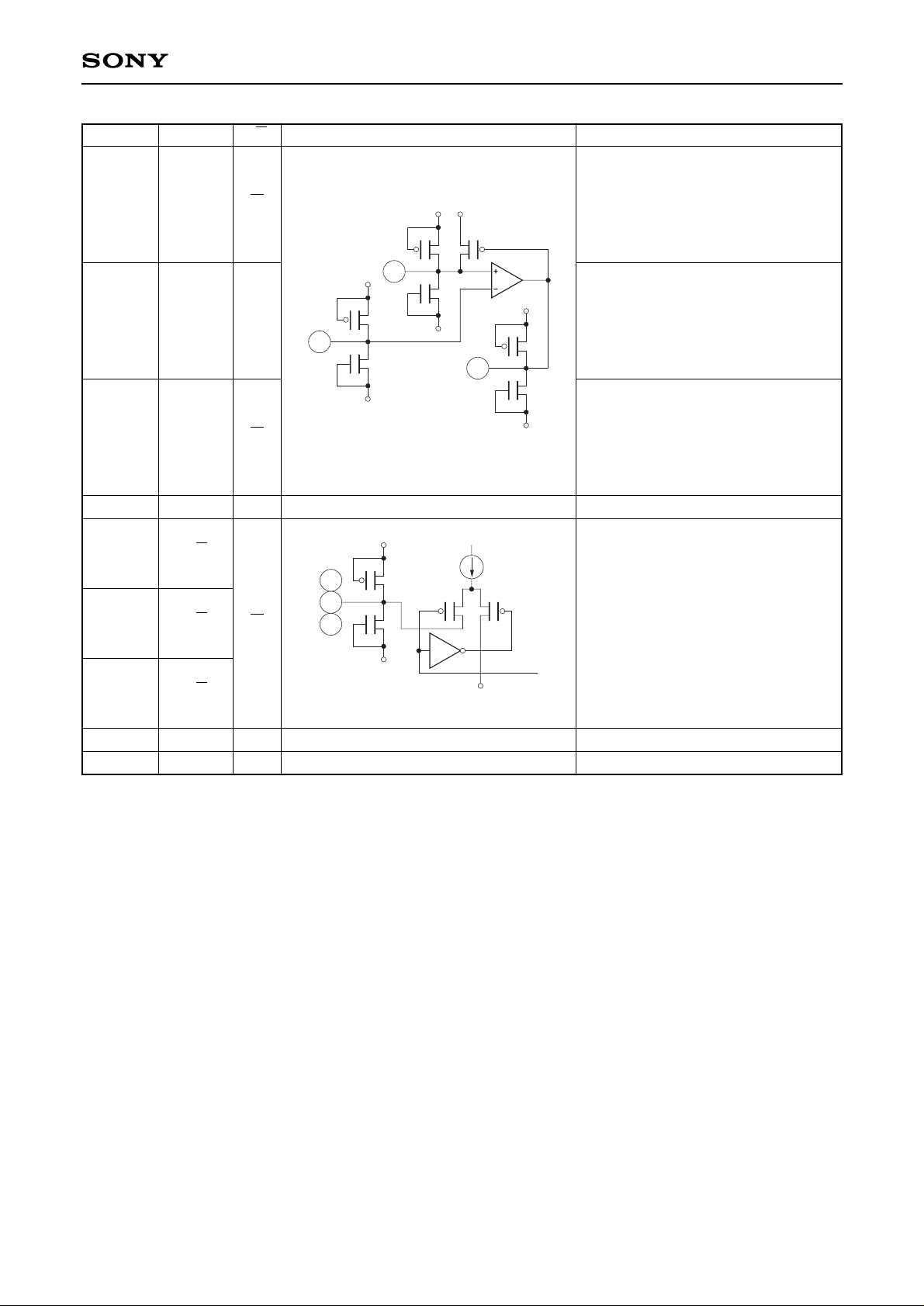
CXD2309Q
Pin No. Symbol I/O Equivalent circuit Description
36
37
38
39 to 41
42
44
46
43, 45, 47
48
IREF
VREF
VG
AVDD
RO
GO
BO
AVSS
DVDD
O
I
O
—
O
—
—
AVDD
AVSS
AVDD
AVSS
37
36
AVDD
AVDD
AVSS
38
AVDD
AVSS
44
46
42
AVSS
Reference current output.
Connect an “RIR” resistor which are
16 times the output resistance
“ROUT”.
Reference voltage input.
Sets an output full-scale value.
Connect an approximately 0.1µF
capacitor.
Analog power supply.
Current output. Output can be
obtained by connecting a resistor
(200 Ω typ.).
Analog ground.
Digital power supply.
—5—
CXD2309Q
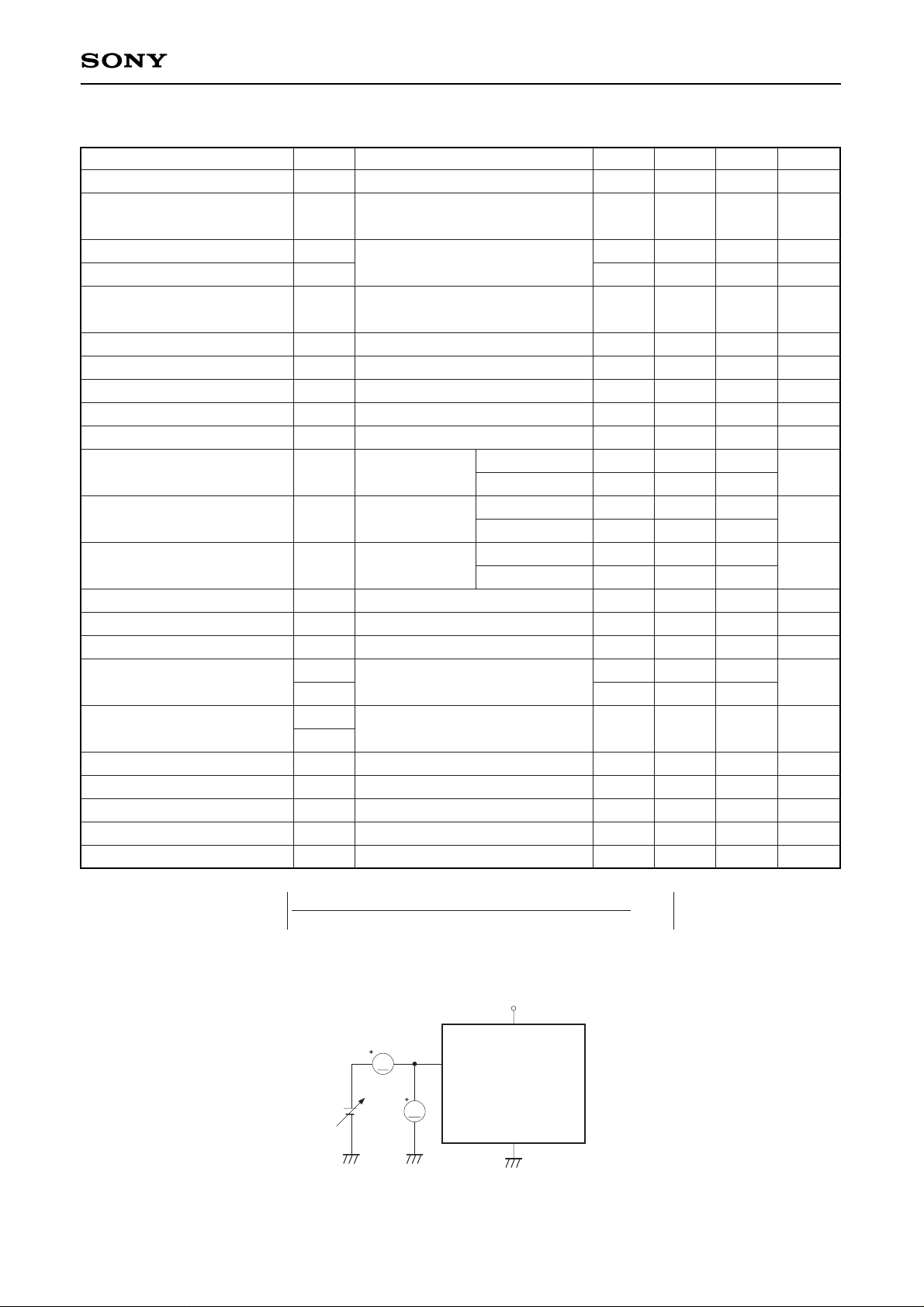
Electrical Characteristics (fCLK=85 MHz, AVDD=DVDD=5 V, ROUT=200 Ω, VREF=2.0 V, RIR=3.3 kΩ, Ta=25°C)
Item
Resolution
Conversion speed
Integral non-linearity error
Differential non-linearity error
Precision guaranteed
output voltage range
Output full-scale voltage
Output full-scale ratio
∗1
Output full-scale current
Output offset voltage
Glitch energy
Crosstalk
SN ratio
Supply current
Analog input resistance
Input capacitance
Output capacitance
Digital input voltage
Digital input current
Setup time
Hold time
Propagation delay time
Rise time
Fall time
Symbol
n
fCLK
EL
ED
VOC
VFS
FSR
IFS
VOS
GE
CT
SNR
IDD
RIN
CI
CO
VIH
VIL
IIH
IIL
ts
th
tPD
tr
tf
Measurement conditions
AVDD=DVDD=4.75 to 5.25 V
Ta=–20 to +85 °C
Endpoint
When “0000000000” data input
ROUT=100 Ω, 1 Vp-p output
When 10 MHz FCLK=50 MHz
sin wave input FCLK=85 MHz
When 1 MHz FCLK=50 MHz
sin wave input FCLK=85 MHz
When 10 MHz FCLK=50 MHz
sin wave output FCLK=85 MHz
VREF
AVDD=DVDD=4.75 to 5.25 V
Ta=–20 to +75 °C
AVDD=DVDD=4.75 to 5.25 V
Ta=–20 to +75 °C
Min.
0
–2.0
–0.5
1.8
1.8
0
9.0
40
50
1
2.15
–5
4
1
Typ.
10
1.92
1.92
9.6
50
42
40
55
50
48
55
125
14
26.5
26.0
Max.
85
2.0
0.5
2.0
2.0
3
10
1
58
9
0.85
5
Unit
bit
MSPS
LSB
LSB
V
V
%
mA
mV
pV•s
dB
dB
mA
MΩ
pF
pF
V
µA
ns
ns
ns
ns
ns
Electrical Characteristics Measurement Circuit
Analog Input Resistance
Measurement Circuit
Digital Input Current
CXD2309Q
+5.25V
AVDD, DVDD
AVSS, DVSS
V
A
}
Full-scale voltage of channel
∗1
Full-scale output ratio =
Average of the full-scale voltage of the channels
–1 × 100 (%)
 Loading...