

Sony CXD2307R Datasheet

—1—
E92928D01
Sony reserves the right to change products and specifications without prior notice. This information does not convey any license by
any implication or otherwise under any patents or other right. Application circuits shown, if any, are typical examples illustrating the
operation of the devices. Sony cannot assume responsibility for any problems arising out of the use of these circuits.
Absolute Maximum Ratings (Ta=25 °C)
• Supply voltage AVDD, DVDD 7V
•Input voltage (All pins)
VIN VDD+0.5 to VSS–0.5 V
• Output current (for each channel)
IOUT 0 to 15 mA
• Storage temperature
Tstg –55 to +150 °C
Recommended Operating Conditions
• Supply voltage AVDD, AVSS 4.75 to 5.25 V
DVDD, DVSS 4.75 to 5.25 V
• Reference input voltage
VREF 1.8 to 2.0 V
• Clock pulse width
TPW1,TPW0 9 ns (min.) to 1.1 µs (max.)
• Operating temperature
Topr –20 to +85 °C
Description
The CXD2307R is a 10-bit high-speed D/A
converter for video band, featuring RGB 3-channel
I/O. This is ideal for use in high-definition TVs and
high-resolution displays.
Features
• Resolution 10-bit
• Maximum conversion speed 50MSPS
• RGB 3-channel I/O
• Differential linearity error ±0.5LSB
• Low power consumption; 300 mW (max.)
• Single +5 V power supply
• Low glitch
• Stand-by function
Structure
Silicon gate CMOS IC
10-bit 50MSPS RGB 3-channel D/A Converter
64 pin LQFP (Plastic)
CXD2307R

—2—
CXD2307R
Block Diagram
4LSB'S
CURRENT
CELLS
6MSB'S
CURRENT
CELLS
CLOCK
GENERATOR
CURRENT CELLS
(FOR FULL SCALE)
4LSB'S
CURRENT
CELLS
6MSB'S
CURRENT
CELLS
CLOCK
GENERATOR
CURRENT CELLS
(FOR FULL SCALE)
4LSB'S
CURRENT
CELLS
6MSB'S
CURRENT
CELLS
CLOCK
GENERATOR
CURRENT CELLS
(FOR FULL SCALE)
BIAS VOLTAGE
GENERATOR
DECODER
LATCHES
DECODER
DECODER
LATCHES
DECODER
DECODER
LATCHES
DECODER
40
39
38
37
36
35
34
33
41
42
43
45
46
47
48
49
52
53
54
55
56
57
58
59
63
64
60
61
62
32
9
10
11
12
13
14
15
16
17
18
19
20
21
22
23
24
25
26
27
28
29
30
2
3
4
5
6
7
8
1
44
50
51
31
(LSB) R0
R1
R2
R3
R4
R5
R6
R7
R8
(MSB) R9
(LSB) G0
G1
G2
G3
G4
G5
G6
G7
G8
(MSB) G9
(LSB) B0
B1
B2
B3
B4
B5
B6
B7
B8
(MSB) B9
BLK
CE
DV
DD
AVDD
AVDD
VGR
RO
RO
RCK
ROR
VRR
IRR
AV
DD
AVDD
VGG
GO
GO
GCK
ROG
VRG
IRG
AVDD
AVDD
VGB
BO
BO
BCK
ROB
VRB
IRB
VB
AV
SS
AVSS
DVSS

—3—
CXD2307R
Pin Configuration
52
53
54
55
56
57
58
59
60
63
64
61
62
49
50
51
20
21
22
23
24
25
26
27
28
29
30
31
32
17
18
19
40
39
38
37
36
35
34
33
4142
43
44
45
46
47
48
2
3
4
5
6
7
8
9
10
11
12
13
14
15
16
1
AVss
RO
RO
AV
DD
AVDD
GO
GO
AV
DD
AVDD
BO
BO
AV
DD
AVDD
DVDD
(LSB) R0
R1
GCK
RCK
CE
BLK
B9
B8
B7
B6
B5
B4
B3
B2
B1
B0 (LSB)
G9
G8
VGB
ROB
VGG
ROG
VGR
ROR
VRB
VRG
VRR
IRB
IRG
IRR
AVss
VB
DVss
BCK
R2
R3
R4
R5
R6
R7
R8
R9
(LSB) G0
G1
G2
G3
G4
G5
G6
G7
Pin Description and Equivalent Circuit
63 to 8
9 to 18
19 to 28
29
30
31
32
33
34
R0 to R9
G0 to G9
B0 to B9
BLK
CE
RCK
GCK
BCK
DVSS
I
—
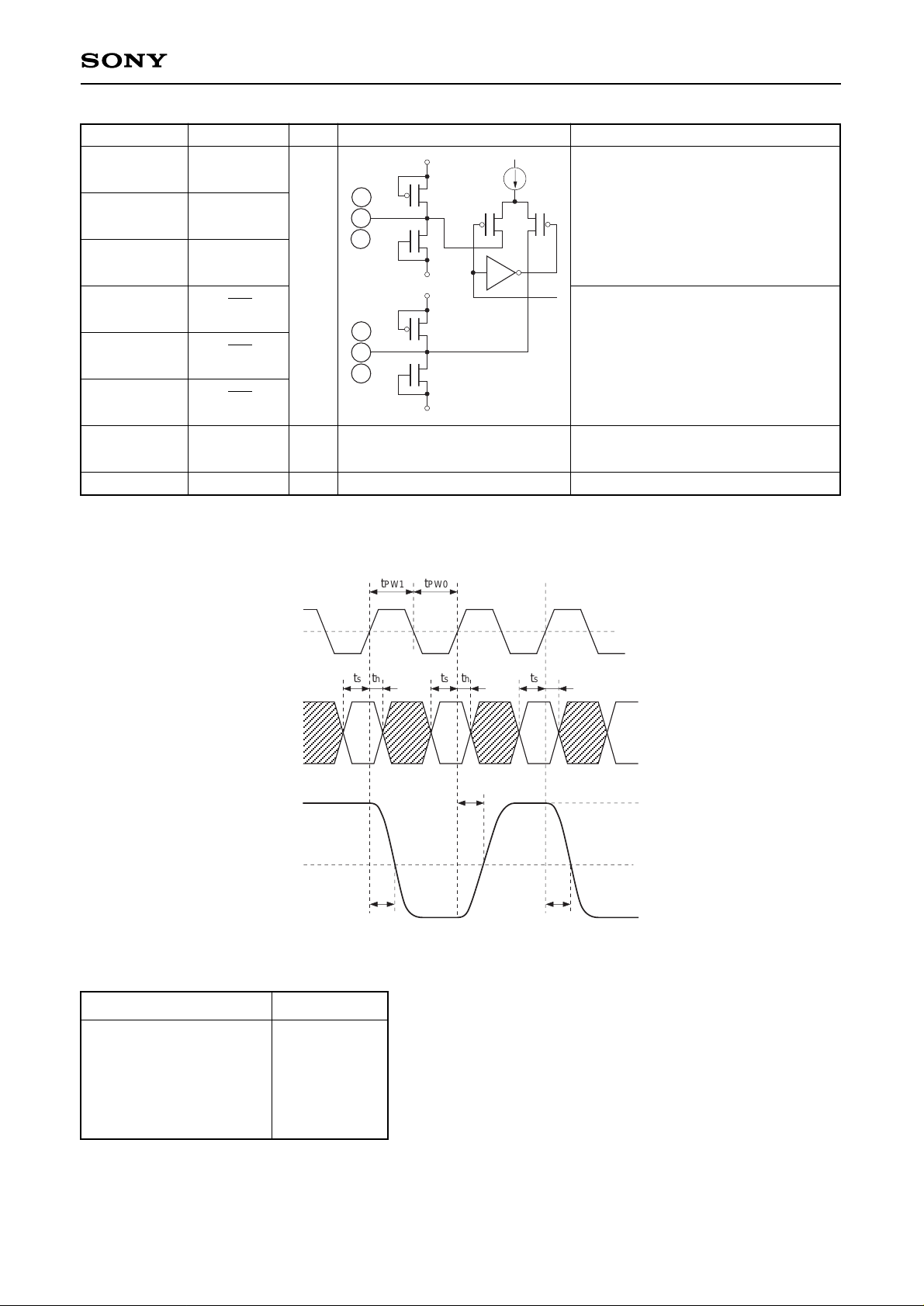
Pin No. Symbol I/O Equivalent circuit Description
DVDD
DVSS
to
33
63
Digital input.
R0 (LSB) to R9 (MSB)
G0 (LSB) to G9 (MSB)
B0 (LSB) to B9 (MSB)
Blanking input.
This is synchronized with the clock
input signal for each channel.
No signal for High (0 V output).
Output generated for Low.
Chip enable pin.
This is not synchronized with the clock
input signal.
No signal at for High (0 V output) to
minimize power consumption.
Clock input.
Digital ground.

—4—
CXD2307R
35
36, 49
43
45
47
44
46
48
37
38
39
40
41
42
VB
AVSS
ROR
ROG
ROB
VGR
VGG
VGB
IRR
IRG
IRB
VRR
VRG
VRB
O
—
O
I
O
I
Pin No. Symbol I/O Equivalent circuit Description
DVDD
DVSS
DVDD
35
AVSS
AVSS
AVDD
AVDD
AVSS
AVDD
AVSS
AVDD
45
47
43
46
48
44
39
37
38
42
41
40
Connect to DVSS with a capacitor of
approximately 0.1 µF.
Analog grounds.
Connect to VGR, VGG, and VGB
with the control method of output
amplitude. See Application Circuit.
Connect a capacitor of approximately
0.1 µF.
Connect to AVSS with a resistance of
3.3 kΩ .
Set output full-scale value (2.0 V).
—5—
CXD2307R
50
54
58
51
55
59
52, 53, 56,
57, 60, 61
62
RO
GO
BO
RO
GO
BO
AVDD
DVDD
O
—
—
Pin No. Symbol I/O Equivalent circuit Description
AVDD
AVSS
AVDD
AVSS
50
54
58
51
55
59
Current output pins. Output can be
retrieved by connecting a resistance
of 200 Ω to AVSS.
Reverse current output pins.
Normally connected to AVSS.
Analog VDD.
Digital VDD.
tPW1 tPW0
ts th ts th ts th
tPD
tPD tPD
CLK
DATA
D/A OUT
1.5V
100%
50%
0%
I/O Correspondence Table (output full-scale voltage: 2.00 V)
Input code Output voltage
MSB LSB
1 1 1 1 1 1 1 1 1 1
:
1 0 0 0 0 0 0 0 0 0
:
0 0 0 0 0 0 0 0 0 0
2.0 V
1.0 V
0 V
Timing Chart
 Loading...