

Sony CXD2303AQ Datasheet

—1—
E98220A89
Sony reserves the right to change products and specifications without prior notice. This information does not convey any license by
any implication or otherwise under any patents or other right. Application circuits shown, if any, are typical examples illustrating the
operation of the devices. Sony cannot assume responsibility for any problems arising out of the use of these circuits.
Absolute Maximum Ratings (Ta=25 °C)
• Supply voltage
AVDD, DVDD 7V
•Input voltage Vin
Digital output pins DVDD+0.5 to DVSS–0.5 V
Other pins AVDD+0.5 to AVSS–0.5 V
• Storage temperature
Tstg –55 to +150 °C
Recommended Operating Conditions
• Supply voltage
AVDD, AVSS 4.75 to 5.25 V
DVDD, DVSS 3.0 to 5.5 V
| DVSS–AVSS | 0 to 100 mV
• Reference input voltage
VARB, VBRB, VCRB 0 or more V
VART, VBRT, VCRT 2.7 or less V
• Analog input
AIN, BIN, CIN 1.7 Vp-p or more
• Clock pulse width
Tpw1, Tpw0 9 ns (min.) to 1.1 µs (max.)
• Operating ambient temperature
Topr –20 to +85 °C
Description
The CXD2303AQ is an 8-bit 3-channel CMOS A/D
converter for video with synchronizing digital clamp
function. The adoption of 2 step-parallel method
achieves low power consumption and a maximum
conversion rates of 50 MSPS.
Features
• Resolution : 8 bit±1/2 LSB (DL)
• Maximum sampling frequency : 50 MSPS
• Low power consumption : 400 mW (at 50 MSPS
Typ.) (Reference current excluded)
• Synchronizing digital clamp function
• Clamp ON/OFF function
• Reference voltage self-bias circuit
• Input CMOS/TTL compatible
• 3-state TTL compatible output
• Single 5 V power supply or dual 5 V/3.3 V power
supplies
• Low input capacitance 15 pF
• Reference impedance : 370 Ω (Typ.)
• Different digital output multiplex format:
– 4 : 4 : 4 format
– 4 : 2 : 2 format
– 4 : 1 : 1 format
Applications
Wide range of applications that require high-speed
A/D conversion such as monitor, TV and VCR.
Structure
Silicon gate CMOS IC
8-bit 3-channel 50 MSPS Video A/D Converter with clamp function
80 pin QFP (Plastic)
CXD2303AQ
—2—
CXD2303AQ
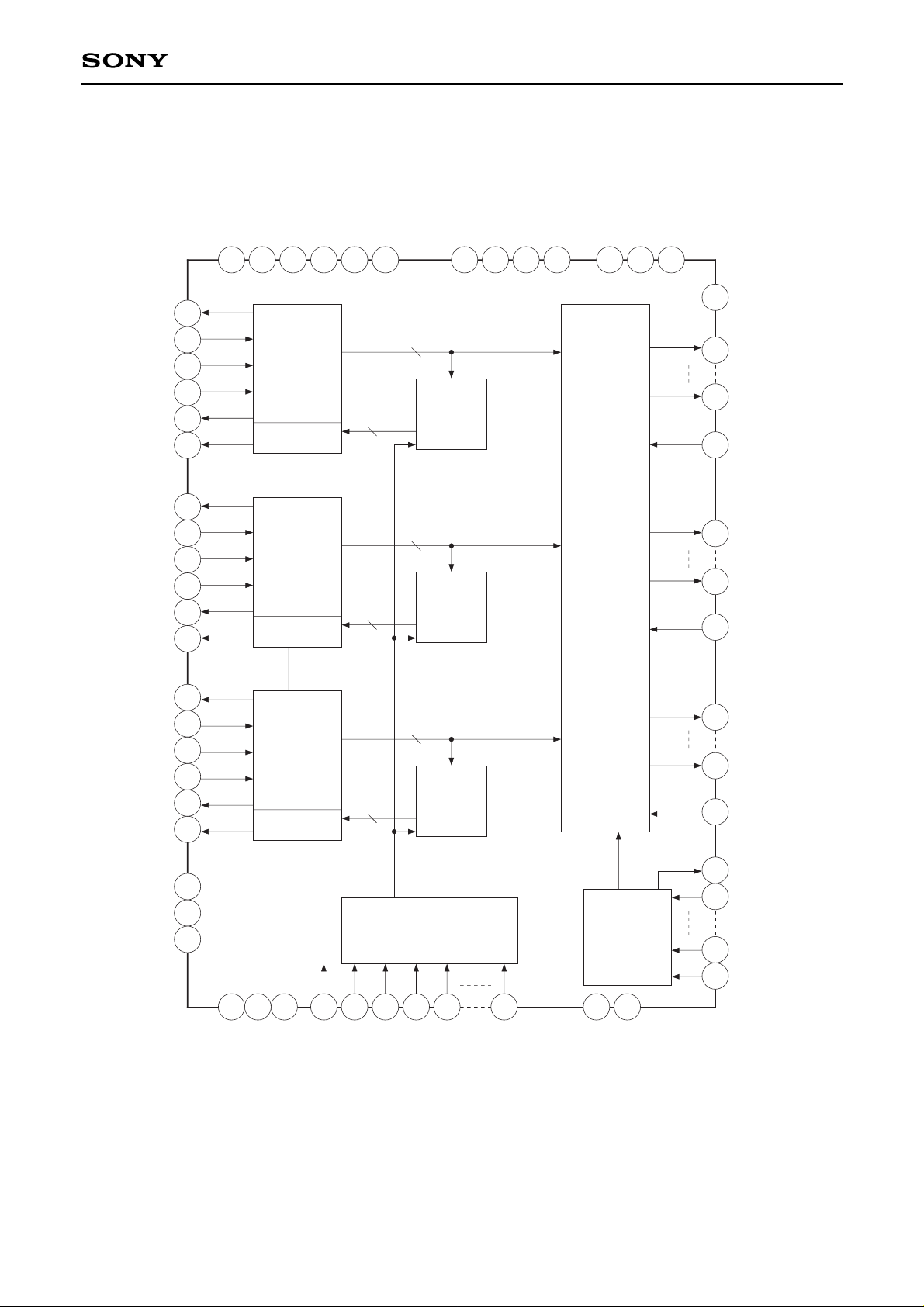
Block Diagram
1 2 1211232235 4241 6862 7130
29
27
25
24
40
38
36
28
26
31
32
39
37
34
33
70
69
67
66
64
63
Decoder
13
72
50
49
21
47
46
80
73
10
3
44
20
45
60 6561 58 43595453 51 5752
Data
Selector
+
Latch
9
9
8
8
9
8
ARTS
ART
AIN
ARB
ARBS
AIO
BRTS
BRT
BIN
BRB
BRBS
BIO
CRTS
CRT
CIN
CRB
CRBS
CIO
AV
SS
AVSS
AVSS
AV
DD
AV
DD
AV
DD
AV
DD
AV
DD
AV
DD
DV
DD
DV
DD
DV
DD
DV
DD
DV
SS
DV
SS
DV
SS
DVSS
A0 (LSB)
A7 (MSB)
XAOE
B0 (LSB)
B7 (MSB)
XBOE
C0 (LSB)
C7 (MSB)
XCOE
TGR
CTL0
CTL2
SY
AV
SS
AV
SS
AV
SS
CLK
CLE
CLP
SEL
REF0
REF3
TEST
TEST
9-bit
DAC
A-ch
8-bit ADC
Digital
Clamp
Circuit
Digital
Clamp
Circuit
9-bit
DAC
B-ch
8-bit ADC
Digital
Clamp
Circuit
9-bit
DAC
C-ch
8-bit ADC
Clamp Control

—3—
CXD2303AQ
Pin Configuration
24
23
22
21
20
19
18
17
16
15
14
13
12
11
10
9
8
7
6
5
4
3
2
1
25
26
27
28
29
30
31
32
33
34
35
36
37
38
39
40
46
45
44
43
42
59
60
61
62
63
50
51
52
53
54
55
56
57
58
64
49
47
48
41
80
79
78
77
76
75
74
73
72
71
70
69
68
67
66
65
BRBS
BRB
AV
SS
BIN
BIO
AV
DD
BRT
BRTS
ARTS
ART
AV
DD
AIO
AIN
AV
SS
ARB
ARBS
AV
SS
CIN
CIO
AV
DD
CRT
CRTS
DV
SS
DV
SS
C0
C1
C2
C3
C4
C5
C6
C7
DV
DD
DV
DD
B0
B1
B2
B3
B4
B5
B6
B7
DV
SS
DV
SS
A0
A1
A2
A3
A4
A5
A6
A7
TGR
DV
DD
DV
DD
AV
SS
CRB
CRBS
AV
DD
AV
SS
AV
SS
TEST
CLE
REF3
REF2
REF1
REF0
CLP
CLK
SEL
SY
CTL2
CTL1
CTL0
XCOE
XBOE
XAOE
TEST
AV
DD
AV
DD
—4—
CXD2303AQ
Pin Description
Pin No. Symbol I/O Equivalent circuit Description
1, 2, 22, 23
13 to 20
3 to 10
73 to 80
21
11, 12, 71, 72
24, 27, 38,
60, 61, 65
25
40
63
26
39
64
31
34
69
32
33
70
28
37
66
DVDD
A0 to A7
B0 to B7
C0 to C7
TGR
DVSS
AVSS
ARBS
BRBS
CRBS
ARB
BRB
CRB
ART
BRT
CRT
ARTS
BRTS
CRTS
AIN
BIN
CIN
—
O
O
—
—
—
—
—
—
I
DVDD
DVSS
Digital power supply.
+5 V or +3.3 V
Digital output.
A0 (LSB) to A7 (MSB)
B0 (LSB) to B7 (MSB)
C0 (LSB) to C7 (MSB)
Trigger output.
See the Tables
and Timing Chart
II
described in the Output Format
section.
Digital ground.
Analog ground.
Shorting these pins to AVSS
generates voltage of about 0.5 V at
the ARB, BRB and CRB pins.
Reference voltage (bottom).
Reference voltage (top).
Shorting these pins to AVDD
generates voltage of about 2.5 V at
the ART, BRT and CRT pins.
Analog input.
AVDD
AVSS
26
40
39
34
33
32
69
63
31
RT
70
64
RB
25
RREF
AVDD
AVSS
28
37
66
—5—
CXD2303AQ
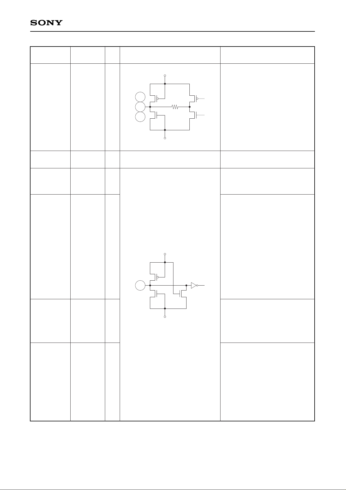
Pin No. Symbol I/O Equivalent circuit Description
29
36
67
30, 35, 41,
42, 62, 68
43
59
44
45
46
47
48
49
50
AIO
BIO
CIO
AVDD
TEST
XAOE
XBOE
XCOE
CTL0
CTL1
CTL2
SY
O
I
I
I
I
AVDD
AVSS
29
36
67
about 200Ω
Analog output.
The digital clamp circuit comprises
a D/A converter whose outputs are
available on these pins.
Analog +5 V power supply.
Normally open.
Pull-down resistors are
incorporated.
Output enable input.
When these pins are Low, data is
output from the digital output pins.
When these pins are High, the
digital output pins are high
impedance.
The A, B and C channels can be
controlled separately.
Also, these pins are not
synchronized with the clock signal.
Pull-down resistors are
incorporated.
Determines the digital output
mode. See the Mode Tables and
Timing Charts.
Pull-down resistors are
incorporated.
Controls the digital output mode
switching timing. The mode is
switched by detecting the transition
point where this pin changes from
Low to High. See the Mode
Tables and Timing Charts for
details.
A pull-down resistor is
incorporated.
AVDD
AVSS
—6—
CXD2303AQ
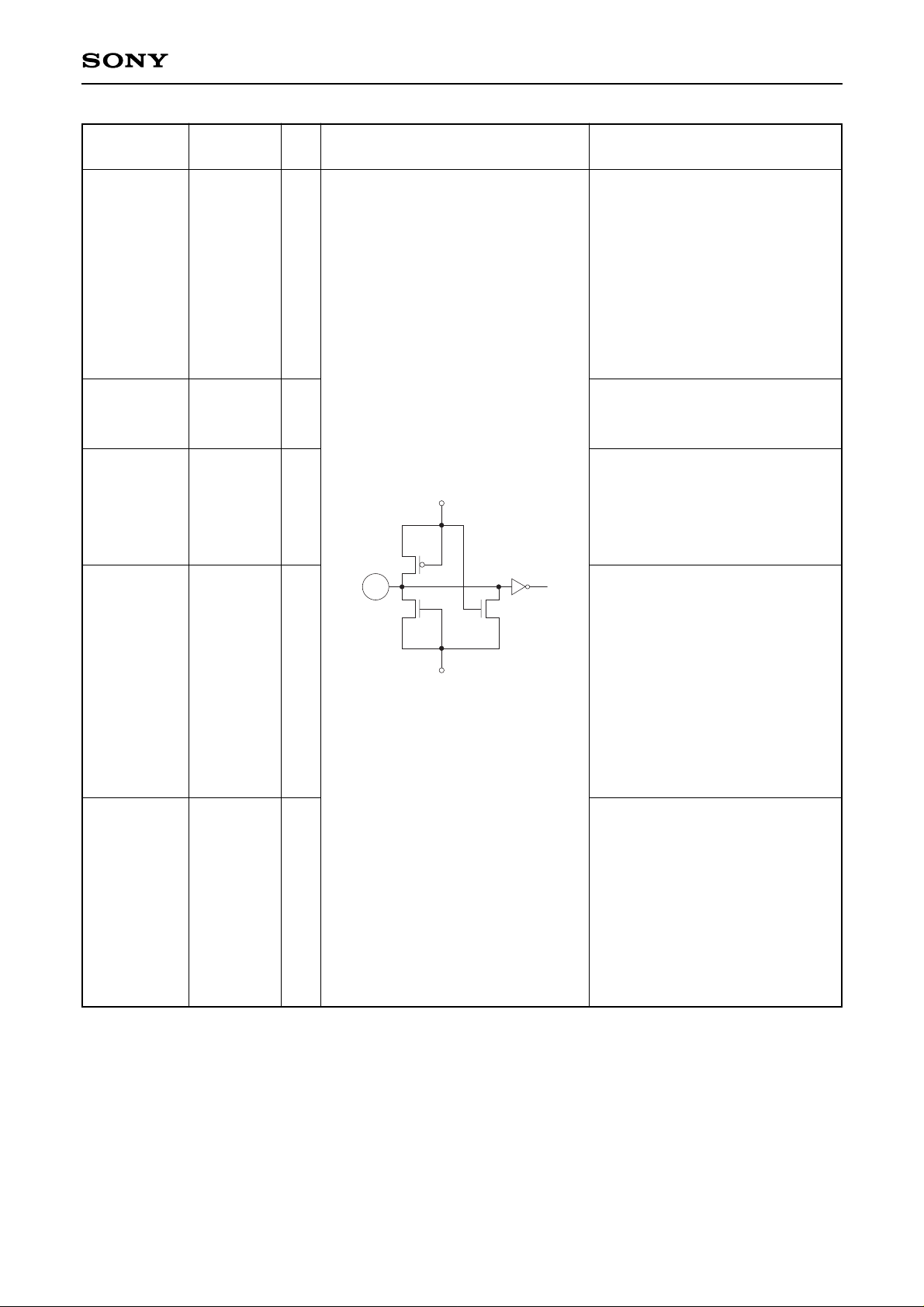
Pin No. Symbol I/O Equivalent circuit Description
51
52
53
54
55
56
57
58
SEL
CLK
CLP
REF0
REF1
REF2
REF3
CLE
I
I
I
I
I
AVDD
AVSS
Controls the CLP signal polarity.
When this pin is Low, CLP is High
active.
When this pin is High, CLP is Low
active.
This pin has a built-in pull-down
resistor.
Clock input.
A pull-down resistor is
incorporated.
Clamp pulse input.
The polarity can be set to either
High or Low by setting SEL.
This pin has a built-in pull-down
resistor.
Determines the clamp circuit
reference data.
See the Mode Tables for the set
data.
These pins are not synchronized
with the clock input signal.
Pull-down resistors are
incorporated.
Clamp enable.
When this pin is Low, the clamp
circuit does not operate.
When this pin is High, the clamp
circuit operates.
A pull-down resistor is
incorporated.
—7—
CXD2303AQ
Digital output
The following table shows the relationship between analog input voltage and digital output code.
Input signal
voltage
VART, VBRT, VCRT
:
:
:
:
VARB, VBRB, VCRB
Step
0
:
127
128
:
255
Digital output code
MSB LSB
1 1 1 1 1 1 1 1
:
1 0 0 0 0 0 0 0
0 1 1 1 1 1 1 1
:
0 0 0 0 0 0 0 0
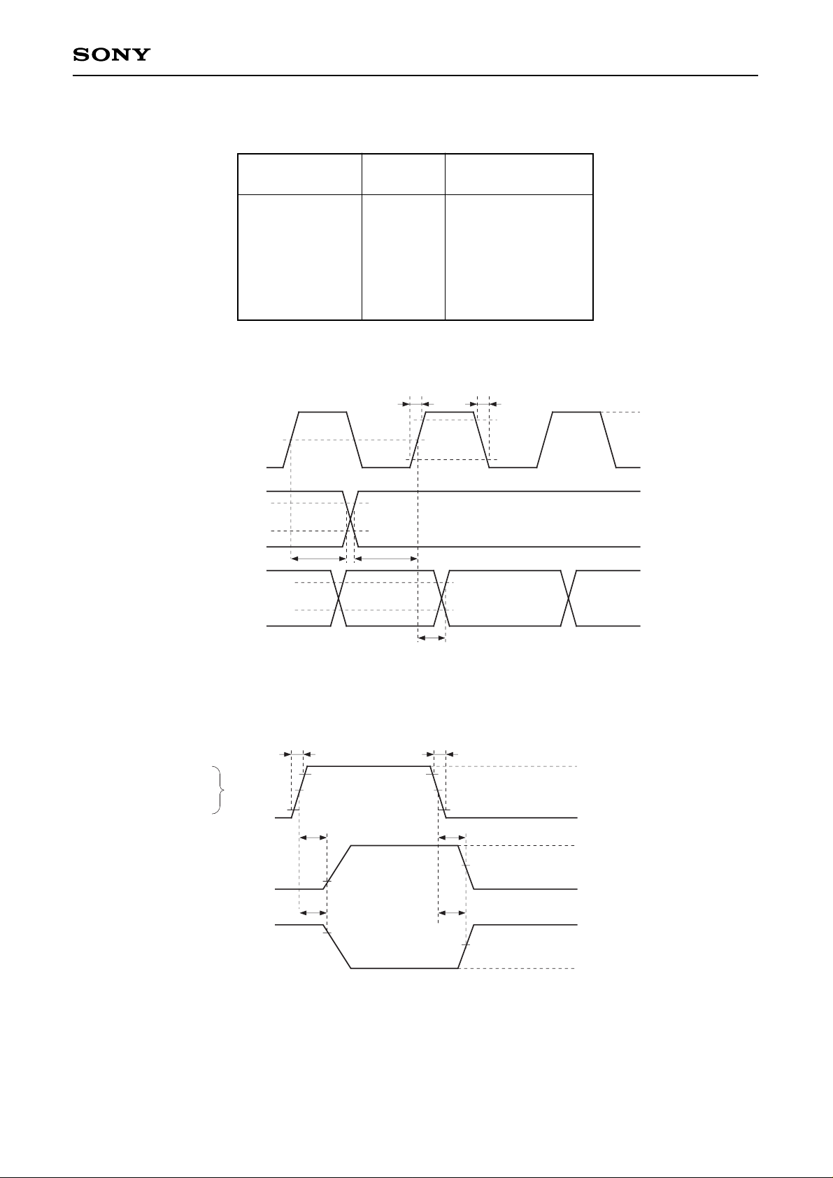
Timing Chart I
Timing Chart I-1.
Timing Chart I-2.
tr
4ns
tf
4ns
90%
10%
3V
0V
1.3V
3V
0V
tH tS
2.2V
0.8V
0.7VDD
0.3VDD
tpLH,
tpHL
Clock
input
Digital
input
Digital
output
90%
10%
3V
0V
1.3V
tr=4.5ns tf=4.5ns
10%
tp
HZ tpZH
1.3V
tpZLtpLZ
VOH
VOL (≠DVSS)
1.3V
90%
VOH (≠DVDD)
V
OL
XAOE
XBOE
XCOE
Output 1
Output 2
input
—8—
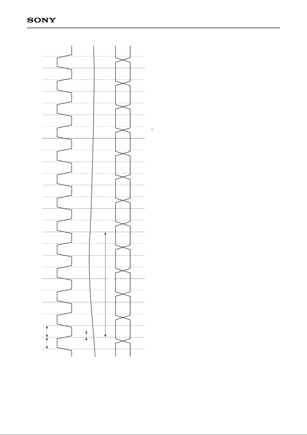
CXD2303AQ
1.3V
Tpw1 Tpw0
tsd
N
N+1
N+2 N+3 N+4
N+5 N+6 N+7
N+8 N+9 N+10 N+11
N–5 N–4 N–3 N–2 N–1 N N+1 N+2 N+3 N+4 N+5 N+6
4.5CLK
Clock
input
Analog
input
Digital
output
: Analog signal sampling point
Timing Chart I-3
—9—
CXD2303AQ
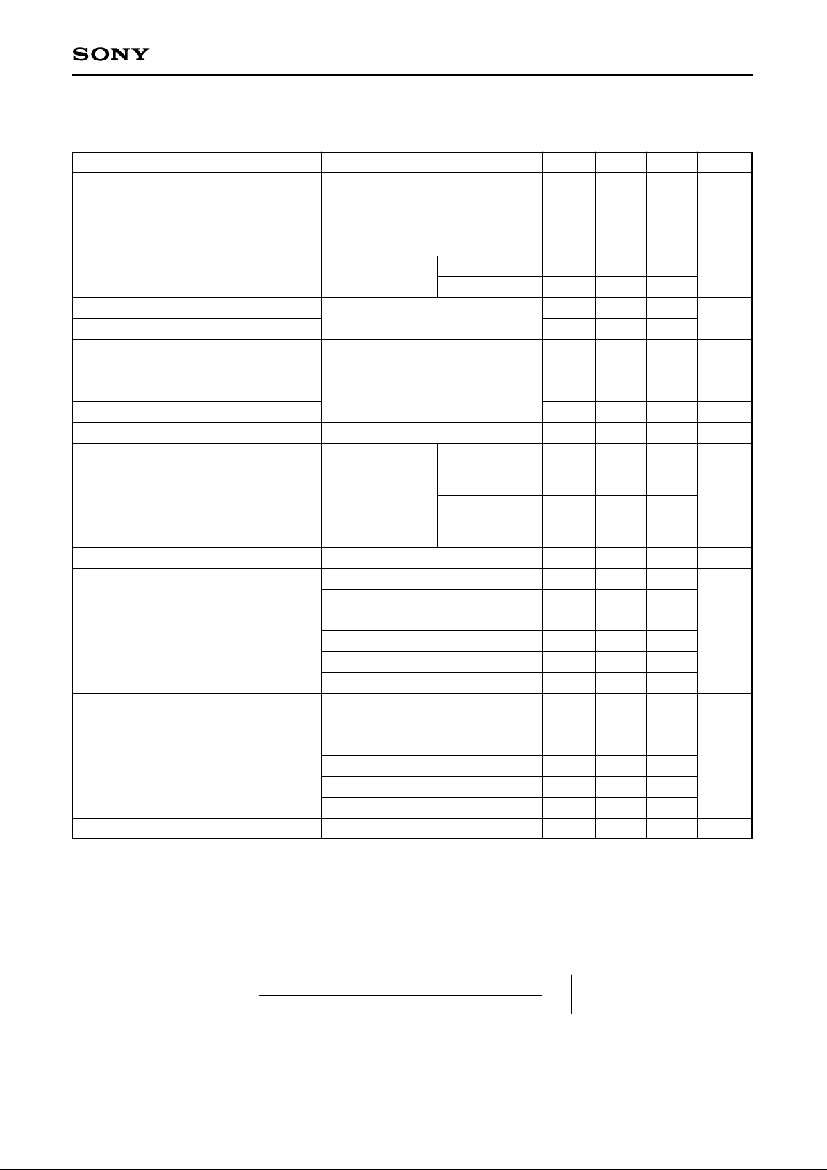
Electrical Characteristics
Analog characteristics (Fc=50 MSPS, AVDD=5 V, DVDD=3 to 5.5 V, VRB=0.5 V, VRT=2.5 V, Ta=25 °C)
Item
Conversion rate
Analog input band width
Differential non-linearity error
Integral non-linearity error
Offset voltage (∗1)
Differential gain error
Differential phase error
Sampling delay
Clamp offset voltage
Full-scale input ratio (∗2)
Signal-to-noise ratio
Spurious free dynamic
range
Cross talk
Symbol
Fc
BW
ED
EL
EOT
EOB
DG
DP
tsd
EOC
SNR
SFDR
CT
Conditions
AVDD=4.75 to 5.25 V
Ta=–20 to +85 °C
VIN=0.5 to 2.5 V
FIN=1 kHz triangular wave
Envelop –1 dB
RIN=33 Ω –3 dB
End point
Potential difference to ART, BRT, CRT
Potential difference to ARB, BRB, CRB
NTSC 40 IRE mod ramp,
Fc=14.3 MSPS
VIN=DC
Ref. Data=
CIN=10 µF
“00010000”
tpcw=2.75 µs
FC=14.3 MHz
Ref. Data=
FCLP=15.75 kHz
“10000000”
FIN=150 kHz
FIN=500 kHz
FIN=1 MHz
FIN=3 MHz
FIN=10 MHz
FIN=20 MHz
FIN=150 kHz
FIN=500 kHz
FIN=1 MHz
FIN=3 MHz
FIN=10 MHz
FIN=20 MHz
FIN=1 MHz sin wave
Min. Typ. Max. Unit
0.5 50 MSPS
60
MHz
100
±0.3 ±0.5
LSB
±0.7 ±1.5
–50 –10
mV
0 40
3 %
1.5 deg
3 ns
±1
LSB
±1
0.5 %
43
42
42
dB
41
38
35
59
59
55
dB
49
44
41
52 dB
(∗1) The offset voltage EOB is a potential difference between ARB, BRB, CRB and a point of position where the
voltage drops equivalent to 1/2 LSB of the voltage when the output data changes from “00000000” to
“00000001”. EOT is a potential difference between ART, BRT, CRT and a potential of point where the
voltage rises equivalent to 1/2 LSB of the voltage when the output data changes from “11111111” to
“11111110”.
(∗2) Full-scale input ratio =
(2 V+EOT–EOB) of each channel
–1 ×100 (%)
Average of (2 V+EOT–EOB) of each channel
—10—
CXD2303AQ
DC characteristics (Fc=50 MSPS, AVDD=5 V, DVDD=5 V or 3.3 V, VRB=0.5 V, VRT=2.5 V, Ta=25 °C)
Item
Analog
Digital
Supply current
Analog
Digital
Reference current
Reference resistance
(RT to RB)
Self-bias
Analog input resistance
Input capacitance
Output capacitance
Digital input voltage
Digital input current
Digital output current
Symbol
IAD+IDD
IAD
IDD
IAD+IDD
IAD
IDD
IREF
R
REF
VRB1
VRT1–VRB1
RIN
CAI1
CAI2
CDIN
CAO
CDO
VIH
VIL
IIH
IIL
IOH
IOL
IOH
IOL
IOZH
IOZL
Conditions
DVDD=5 V
DVDD=3.3 V
NTSC ramp DVDD=5 V
wave input
DVDD=3.3 V
CLE=Low
For every channel
For every channel
Shorts AVSS and ARBS, BRBS,
CRBS.
Shorts AVDD and ARTS, BRTS,
CRTS.
Fc=50 MHz
AIN, BIN, CIN Fc=35 MHz
Fc=20 MHz
AIN, BIN, CIN,
VIN=1.5 V+0.07 Vrms
ARTS, ART, ARB, ABFS,
BRTS, BRT, BRB, BRBS,
CRTS, CRT, CRB, CRBS
Digital input pin
AIO, BIO, CIO
Digital output pin
AVDD=4.75 to 5.25 V
DVDD=3 to 5.5 V
Ta=–20 to +75 °C
VI=0 V to AVDD
Ta=–20 to +75 °C
XOE=0 V
VOH=DV
DD–0.8 V
DVDD=5 V
VOL=0.4 V
Ta=–20 to 75 °C
XOE=0 V
VOH=DV
DD–0.8 V
DVDD=3.3 V
VOL=0.4 V
Ta=–20 to 75 °C
XOE=3 V
VOH=DV
DD
DVDD=3 to 5.5 V
Ta=–20 to 75 °C
VOL=0 V
Min. Typ. Max. Unit
80 100
70 90
5 10 mA
70 90
60 80
5 10
4.1 5.4 7.7 mA
260 370 480 Ω
0.50 0.54 0.58
V
1.80 1.92 2.04
13
16 kΩ
30
15
pF
9
9
11
pF
11
2.2
V
0.8
–40 240 µA
–2
4
mA
–1.2
2.4
–40 40 µA
NTSC ramp
wave input
CLE=High
F
CLP
=15.75 kHz
—11—
CXD2303AQ
Timing (Fc=50 MSPS, AVDD=5 V, DVDD=5 V or 3.3 V, VRB=0.5 V, VRT=2.5 V, Ta=25 °C)
DC Characteristic (Continue)
Item
Output data delay
Tri-state output
enable time
Tri-state output
disable time
Setup time
Hold time
Pulse width
Symbol
tpLH
tpHL
tpLH
tpHL
tpZH
tpZL
tpZH
tpZL
tpHZ
tpLZ
tpHZ
tpLZ
tS
tH
tH
Conditions
DVDD=5 V
CL=15 pF
XOE=0 V
DVDD=3.3 V
RL=1 kΩ DVDD=5 V
CL=15 pF
XOE=3 V → 0 V DVDD=3.3 V
RL=1 kΩ DVDD=5 V
CL=15 pF
XOE=0 V → 3 V DVDD=3.3 V
CTL0 to 2, CLP, SY
CLK conversion
CLP
SY
Min. Typ. Max. Unit
4.5
8.5
11.0
7.4
ns
3.8
10.0
13.8
6.7
4.2
7.1
11.3
8.0
ns
3.5
8.4
12.8
7.2
3.6
6.8
9.5
6.3
ns
2.9
6.8
10.5
6.0
3.5 ns
4.5 ns
2
Cycle
1
Electrical Characteristics Measurement Circuit
Output data delay measurement circuit Tri-state output measurement circuit
CL
To output pin
Measurement
point
CL
To output pin
RL
RL
Measurement point DVDD
Note) CL includes capacitance of probes.
Conditions
XOE=0 V IOH=–2 mA
DVDD=5 V
Ta=–20 to 75 °C IOL=4 mA
XOE=0 V IOH=–1.2 mA
DVDD=3.3 V
Ta=–20 to 75 °C IOL=2.4 mA
Item
Digital output voltage
Symbol
VOH
VOL
VOH
VOL
Min. Typ. Max. Unit
DVDD
–0.8
0.4
V
DVDD
–0.8
0.4
—12—
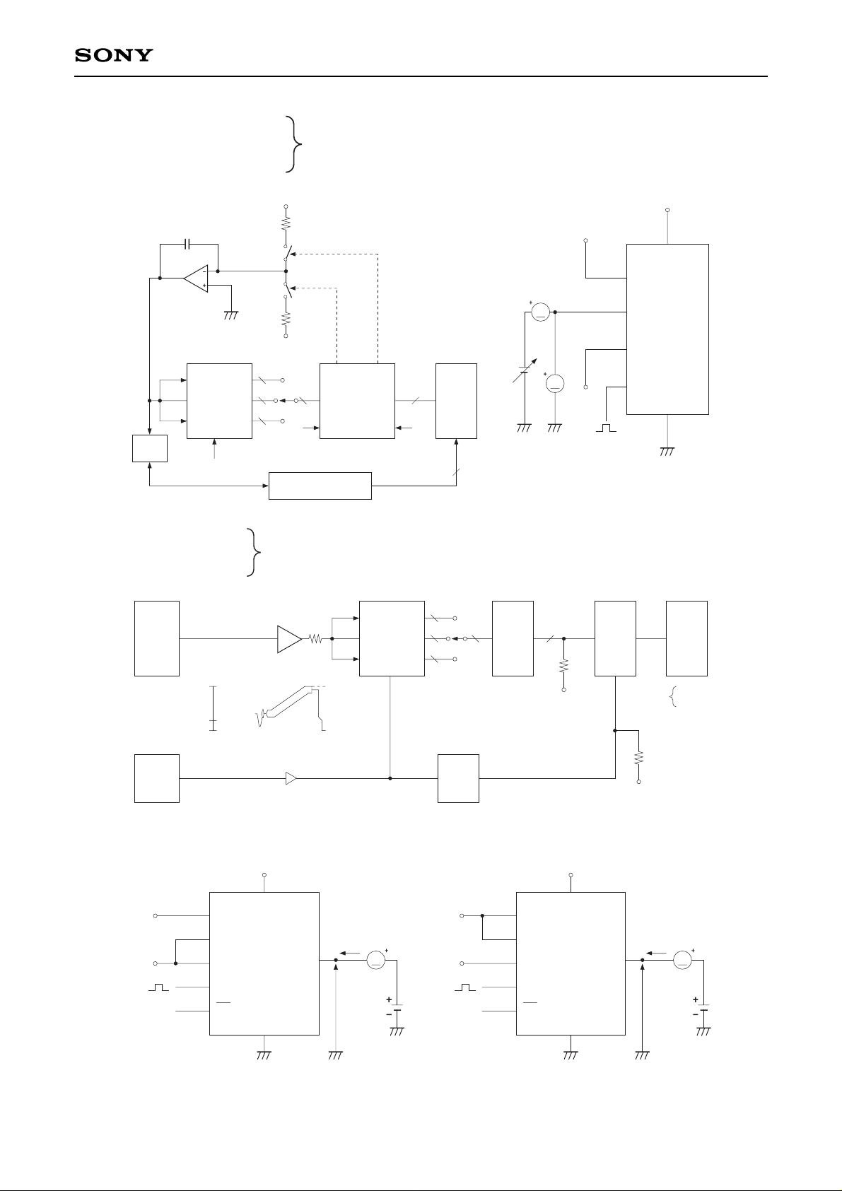
CXD2303AQ
Integral non-linearity error Analog input resistance measurement circuit
Differential non-linearity error
measurement
Offset voltage
circuit
Differential gain error
measurement circuit
Differential phase error
Digital output current measurement circuit
DVM
+V
–V
AIN
A8
to
A1
A0
B8
to
B1
B0
A<B A>B
COMPARATOR
8
S1
S2
S1 : ON
IF A<B
S2 : ON IF B>A
BUFFER
8
“1”
CLK (50MHZ)
CONTROLLER
8
000···00
TO
111···10
BIN
CIN
8
8
A
B
C
8
“0”
ART, BRT, CRT
AIN, BIN, CIN
ARB, BRB, CRB
CLK
AV
DD, DVDD
AVSS, DVSS
+5V
0.5V
A
V
2.5V
DUT
CXD2303AQ
AIN
8
BIN
CIN
8
8
A
B
C
8
TTL
↓
ECL
AMP
2.5V
0.5V
40 IRE
MODULATION
BURST
SYNC
100
0
–40
IRE
NTSC
SIGNAL
SOURCE
620
–5.2V
8
CX20202A-1
VECTOR
SCOPE
D.G
D.P.
S.G.
(CW)
TTL
↓
ECL
FC
CLK
620
–5.2V
10-bit
D/A
DUT
CXD2303AQ
ART, BRT, CRT
AIN, BIN, CIN
ARB, BRB, CRB
CLK
AV
DD, DVDD
AVSS, DVSS
2.5V
OE
0.5V
Data
out
A
IOL
VOL
ART, BRT, CRT
AIN, BIN, CIN
ARB, BRB, CRB
CLK
2.5V
OE
0.5V
Data
out
A
IOH
VOL
AVDD, DVDD
AVSS, DVSS
+4.75V+4.75V
 Loading...