


CXD2302Q
8-bit 50MSPS Video A/D Converter with Clamp Function
Description
The CXD2302Q is an 8-bit CMOS A/D converter
for video with synchronizing clamp function. The
adoption of 2 step-parallel method achieves low
power consumption and a maximum conversion rate
of 50MSPS.
Features
• Resolution: 8 bit ± 1/2LSB (DL)
• Maximum sampling frequency: 50MSPS
• Low power consumption: 125mW (at 50MSPS typ.)
(reference current excluded)
• Synchronizing clamp function
• Clamp ON/OFF function
• Reference voltage self-bias circuit
• Input CMOS/TTL compatible
• 3-state TTL compatible output
• Single 5V power supply or dual 5V/3.3V power supply
• Low input capacitance: 15pF
• Reference impedance: 370Ω (typ.)
Absolute Maximum Ratings (Ta = 25°C)
• Supply voltage VDD 7V
•Reference voltage VRT,VRBVDD + 0.5 to Vss – 0.5V
• Input voltage VIN VDD + 0.5 to Vss – 0.5V
(Analog)
• Input voltage VI VDD + 0.5 to Vss – 0.5V
(Digital)
• Output voltage VO VDD + 0.5 to Vss – 0.5V
(Digital)
• Storage temperature
32 pin QFP (Plastic)
Tstg –55 to +150 °C
Applications
Wide range of applications that require high-speed
A/D conversion such as TV and VCR.
Structure
Silicon gate CMOS IC
Recommended Operating Conditions
• Supply voltage AVDD, AVss 4.75 to 5.25 V
DVDD, DVss 3.0 to 5.5 V
| DVss – AVss | 0 to 100 mV
• Reference input voltage
VRB 0 and above V
VRT 2.7 and below V
• Analog input VIN 1.7Vp-p above
• Clock pulse width
TPW1, TPW0 9ns (min) to 1.1µs (max)
• Operating ambient temperature
Topr –40 to +85 °C
Sony reserves the right to change products and specifications without prior notice. This information does not convey any license by
any implication or otherwise under any patents or other right. Application circuits shown, if any, are typical examples illustrating the
operation of the devices. Sony cannot assume responsibility for any problems arising out of the use of these circuits.
– 1 –
E94102E78-PS
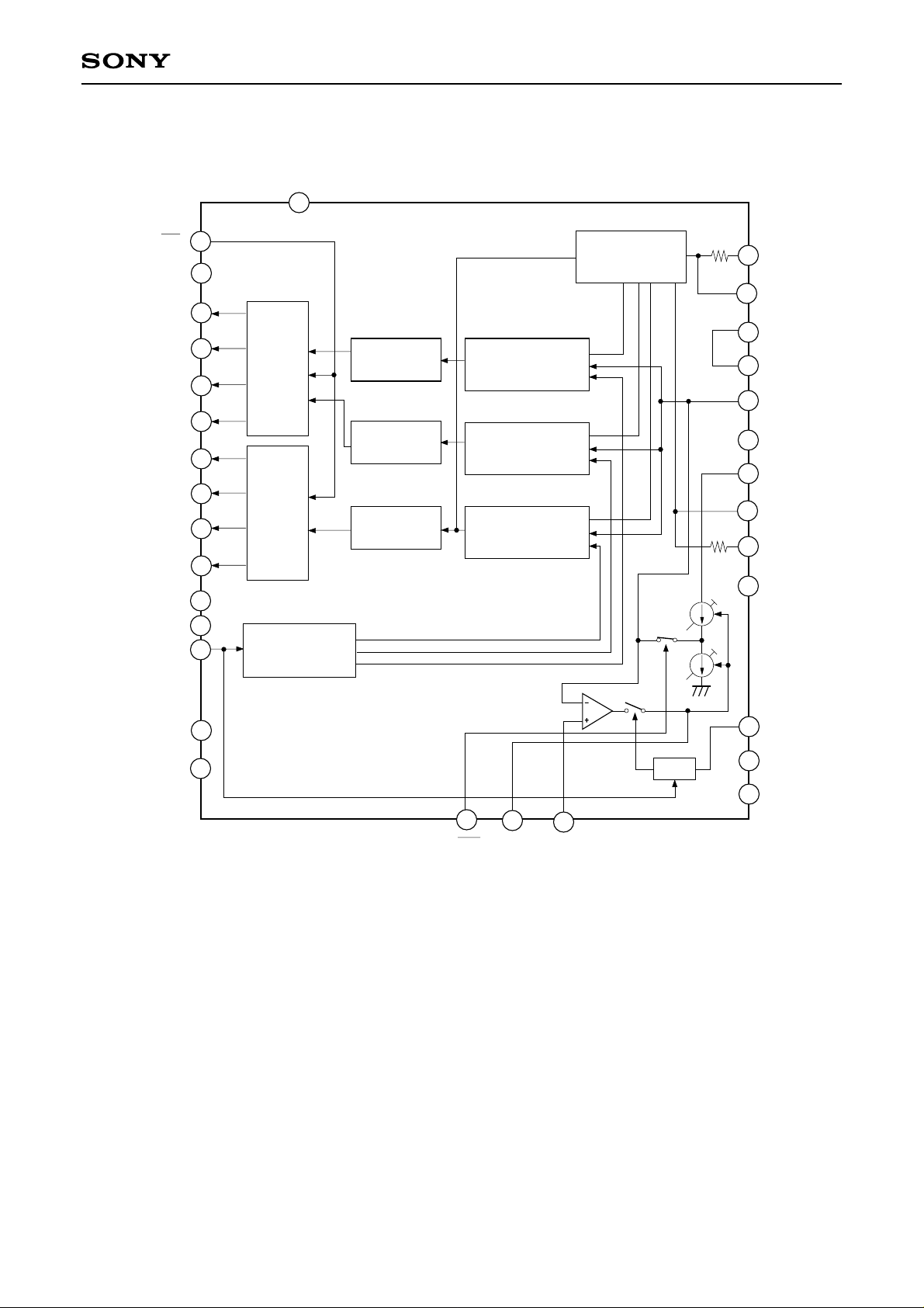
Block Diagram
OE
DVss
D0 (LSB)
D1
D2
D3
D4
D5
D6
D7 (MSB)
DVDD
TEST (OPEN)
CLK
30
10
12
31
11
CXD2302Q
DVss
28
Reference supply
1
2
3
4
5
6
7
8
Lower
data
latch
Upper
data
latch
Clock generator
Lower encoder
(4 BIT)
Lower encoder
(4 BIT)
Upper encoder
(4 BIT)
Lower
sampling comparator
(4 BIT)
Lower
sampling comparator
(4 BIT)
Upper
sampling comparator
(4 BIT)
25
24
23
22
21
20
19
18
17
16
VRBS
VRB
AVss
AVss
VIN
AVDD
AVDD
VRT
VRTS
AVDD
TEST (OPEN)
NC
32
15
14
13
CLP
NC
NC
9
D-FF
29
CLE CCP V
27
26
REF
– 2 –
Pin Description
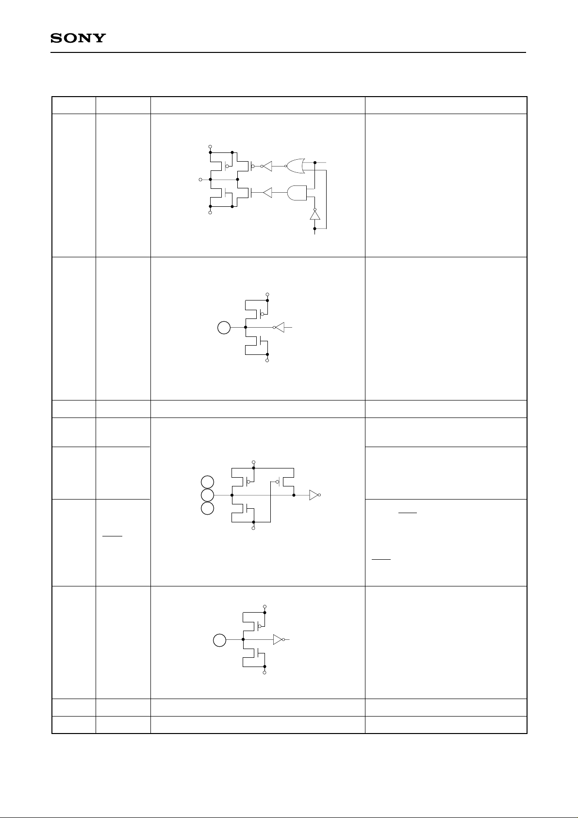
Pin No. Symbol Equivalent circuit Description
DVDD
Di
1 to 8
D0 to D7
D0 (LSB) to D7 (MSB) output
DVSS
DVDD
CXD2302Q
9
10
11
TEST
DVDD
TEST
15 CLP
29 CLE
11
15
29
9
DVSS
Leave open for normal use.
Digital power supply +5V or +3.3V
Leave open for normal use.
Pull-up resistor is built in.
AVDD
Input the clamp pulse.
Clamps the signal voltage during
Low interval. Pull-up resistor is
built in.
The clamp function is enabled
when CLE = Low.
AVSS
The clamp function is set to off
and the converter functions as a
normal A/D converter when
CLE = High.
Pull-up resistor is built in.
AVDD
12
13, 14, 32
16, 19, 20
CLK
12
Set to Low level when no clock is
input.
Clock input.
AVSS
NC
AVDD Analog power supply +5V
– 3 –
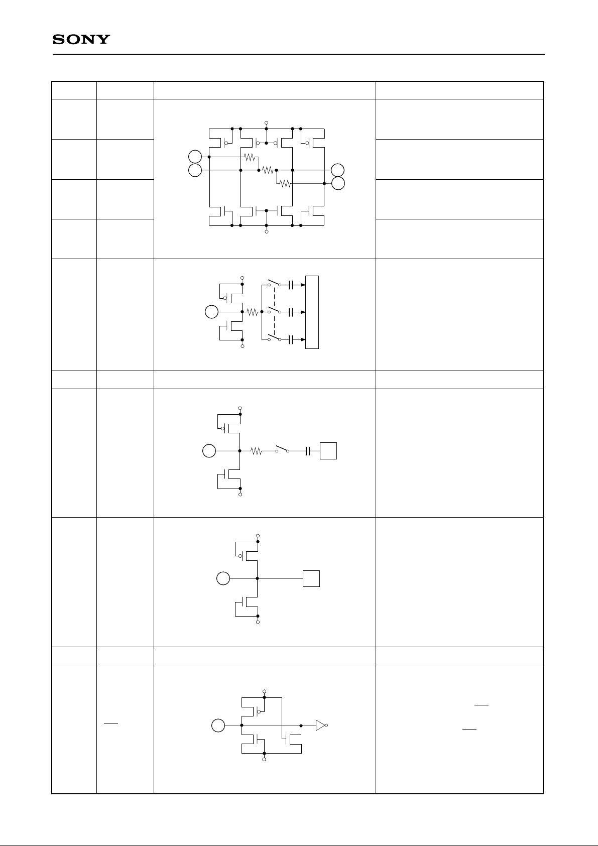
Pin No. Symbol Equivalent circuit Description
CXD2302Q
Generates approximately +2.5V
when shorted with AVDD.
Reference voltage (top)
Reference voltage (bottom)
Generates approximately +0.6V
when shorted with AVSS.
AVDD
AVSS
AVDD
RT
AVDD
Rref
AVSS
24
B
R
25
17 VRTS
18 VRT
17
18
24 VRB
25 VRBS
21 VIN Analog input
22, 23
AVSS Analog ground
21
26 VREF
27 CCP
28, 31
DVSS Digital ground
30 OE
26
30
27
Clamp reference voltage input.
Clamps so that the reference
voltage and the input signal during
clamp interval are equal.
AVSS
AVDD
Integrates the clamp control
voltage.
The relationship between the
changes in CCP voltage and in VIN
voltage is positive phase.
AVSS
AVDD
Data is output when OE = Low.
Pins D0 to D7 are at high
impedance when OE = High.
Pull-down resistor is built in.
AVSS
– 4 –
Digital output
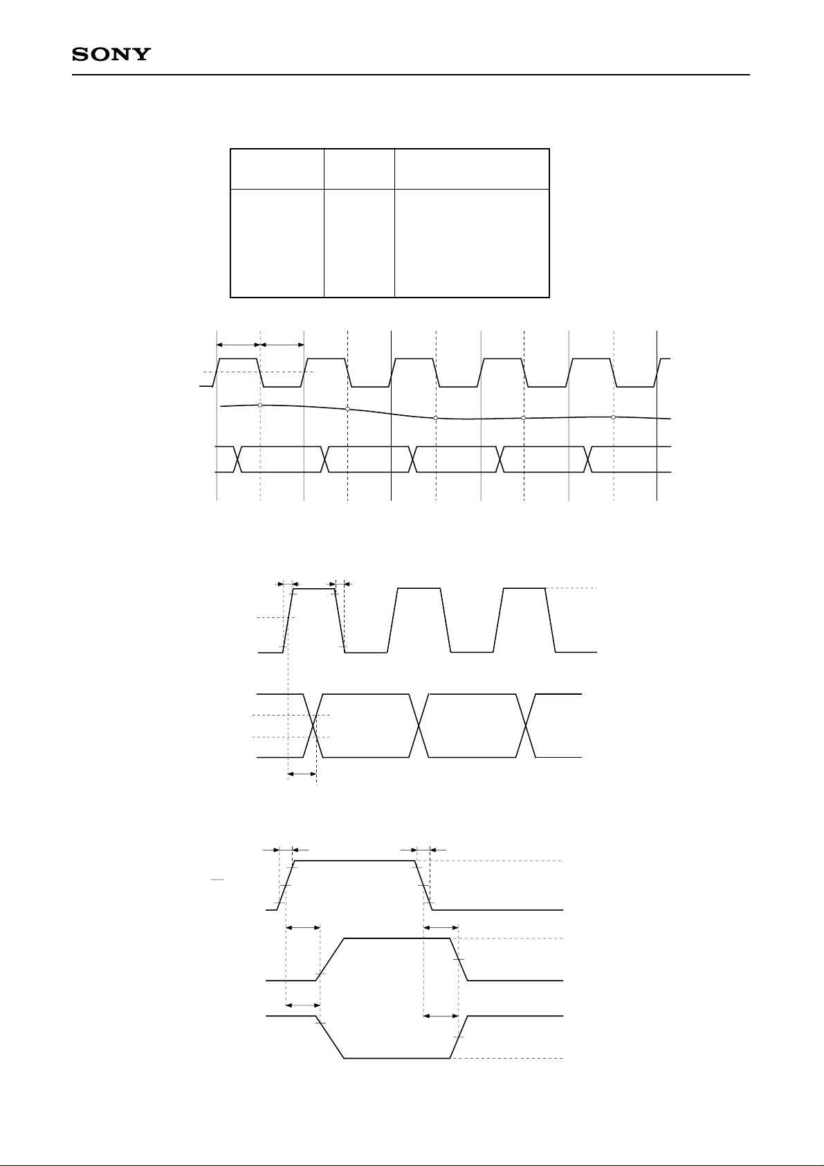
The following table shows the relationship between analog input voltage and digital output code.
CXD2302Q
Timing Chart I
Clock 1.3V
Analog input
Data output
Clock
Input signal
voltage
TPW1 TPW0
1.3V
VRT
:
:
:
:
VRB
N
4ns
Step
0
:
127
128
:
255
N + 1
Digital output code
MSB LSB
1 1 1 1 1 1 1 1
:
1 0 0 0 0 0 0 0
0 1 1 1 1 1 1 1
:
0 0 0 0 0 0 0 0
N + 2 N + 3 N + 4
N + 1NN – 1N – 2N – 3
O: Analog signal sampling point
Timing Chart I-1.
tr
tf
4ns
90%
3V
Data output
DD
0.7DV
0.3DVDD
OE input
Output 1
Output 2
10%
tpLH,
tpHL
Timing Chart I-2.
tr = 4.5ns tf = 4.5ns
90%
1.3V
tpZLtpLZ
10%
tpHZ
tpZH
90%
10%
1.3V
1.3V
0V
3V
0V
OH
V
VOL (≠ DVSS)
V
OH (≠ DVDD)
V
OL
Timing Chart I-3.
– 5 –
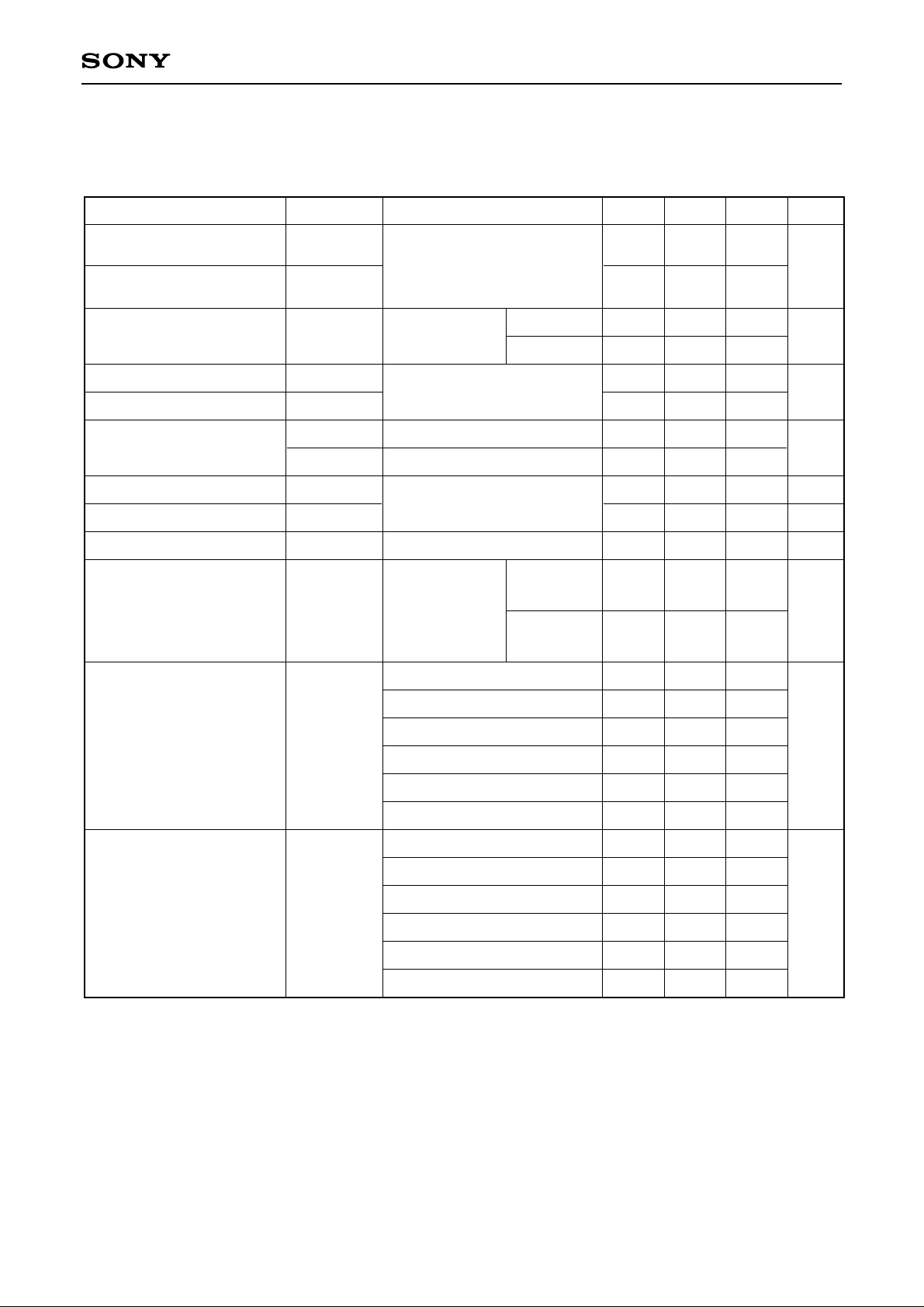
Electrical Characteristics
CXD2302Q
Analog characteristics
Item Symbol Conditions Min. Typ. Max. Unit
Max. conversion rate
Min. conversion rate
Analog input band width
Differential non-linearity error
Integral non-linearity error
Offset voltage
Differential gain error
Differential phase error
Sampling delay
Clamp offset voltage
∗1
∗2
(Fc = 50MHz, AVDD = 5V, DVDD = 3 to 5.5V, VRB = 0.5V, VRT = 2.5V, Ta = 25°C)
Fc max.
Fc min.
BW
ED
EL
EOT
EOB
DG
DP
tsd
EOC
AVDD = 4.75 to 5.25V
Ta = –40 to +85°C,
VIN = 0.5 to 2.5V
fIN = 1kHz triangular wave
Envelope
RIN = 33Ω
End point
Potential difference to VRT
Potential difference to VRB
NTSC 40 IRE mod ramp
Fc =14.3MSPS
VIN = DC
CIN = 10µF
–1dB
–3dB
VREF = 0.5V
tpcw = 2.75µs
Fc = 14.3MHz
Fclp = 15.75kHz
VREF = 2.5V
50
–70
20
02040
02040
65
60
100
±0.3
+0.7
–50
40
3
1.5
0
0.5
±0.5
±1.5
–30
60
MSPS
MHz
LSB
mV
%
deg
ns
mV
FIN = 100kHz
FIN = 500kHz
Signal-to-noise ratio
Spurious free dynamic
range
∗1
The offset voltage EOB is a potential difference between VRB and a point of position where the voltage
drops equivalent to 1/2 LSB of the voltage when the output data changes from “00000000” to “00000001”.
EOT is a potential difference between VRT and a potential of point where the voltage rises equivalent to
1/2LSB of the voltage when the output data changes from “11111111” to “11111110”.
∗2
Clamp offset voltage varies individually. When using with R, G, B 3 channels, color sliding may be
generated.
SNR
FSDR
FIN = 1MHz
FIN = 3MHz
FIN = 10MHz
FIN = 25MHz
FIN = 100kHz
FIN = 500kHz
FIN = 1MHz
FIN = 3MHz
FIN = 10MHz
FIN = 25MHz
45
44
44
43
38
32
51
46
49
46
45
45
dB
dB
– 6 –
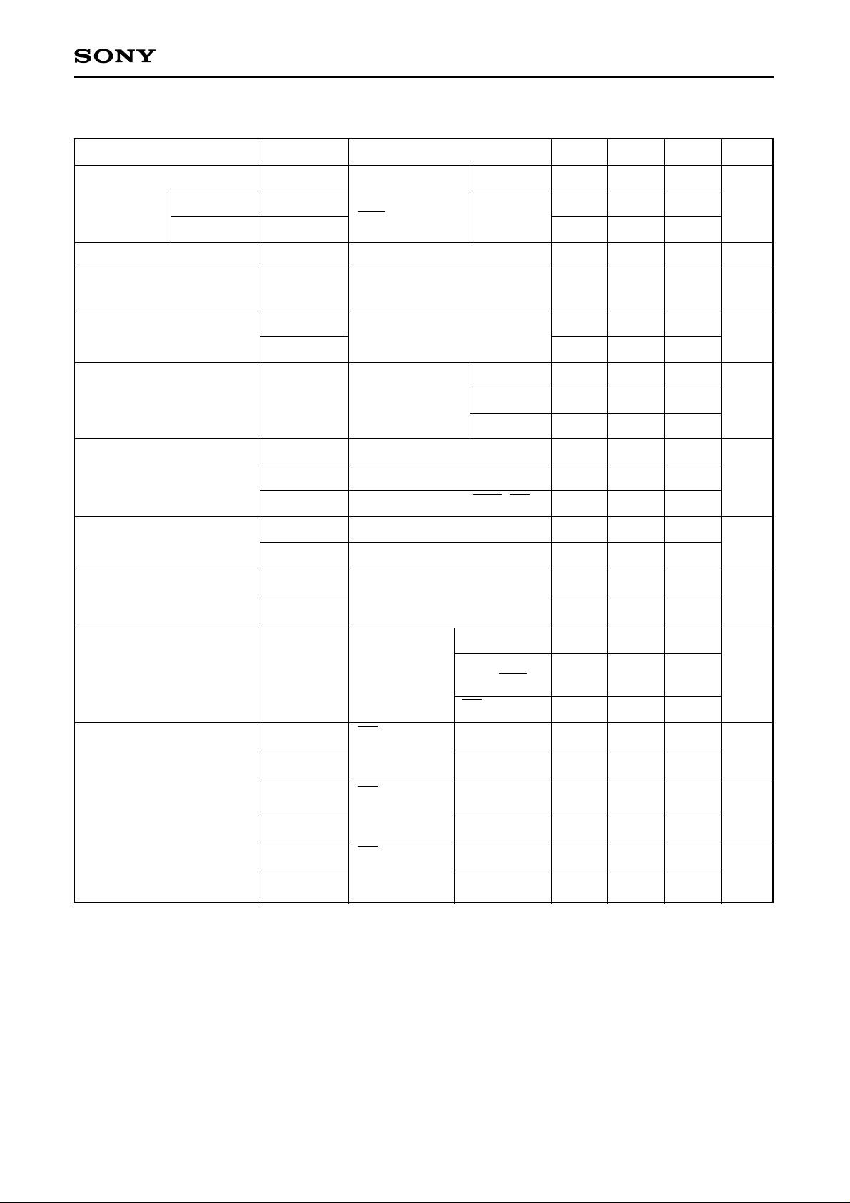
CXD2302Q
DC characteristics
Item Symbol Conditions Min. Typ. Max. Unit
Supply
current
Analog
Digital
Reference current
Reference resistance
(VRT – VRB)
Self-bias voltage
Analog input resistance
Input capacitance
Output capacitance
(Fc = 50MHz, AVDD = 5V, DVDD = 5V or 3.3V, VRB = 0.5V, VRT = 2.5V, Ta = 25°C)
IAD + IDD
IAD
IDD
IREF
RREF
VRB
VRT – VRB
RIN
CAI1
CAI2
CDIN
CAO
NTSC ramp
DVDD = 5V
wave input
CLE = 0V
DVDD = 3.3V
Shorts VRTS and AVDD
Shorts VRBS and AVSS
Fc = 50MHz
VIN
Fc = 35MHz
Fc = 20MHz
VIN, VIN = 1.5V + 0.07Vrms
VRTS, VRT, VRB, VRBS, VREF
TEST, CLK, CLP, CLE, OE
CCP
4.1
260
0.52
1.80
25
23
2
5.4
370
0.56
1.92
13
16
30
15
36
33
3
7.7
480
0.60
2.04
11
11
11
mA
mA
Ω
V
kΩ
pF
pF
CDO
D0 to D7, TEST
11
Digital input voltage
Digital input current
Digital output current
VIH
VIL
IIH
IIL
IOH
IOL
IOH
IOL
IOZH
IOZL
AVDD = 4.75 to 5.25V
DVDD = 3 to 5.5V
Ta = –40 to +85°C
CLK
VI = 0V to AVDD
Ta = –40 to +85°C
TEST,
CLP, CLE
OE
OE = 0V
VOH = DVDD – 0.8V
DVDD = 5V
Ta = –40 to +85°C
OE = 0V
VOL = 0.4V
VOH = DVDD – 0.8V
DVDD = 3.3V
Ta = –40 to +85°C
OE = 3V
VOL = 0.4V
VOH = DVDD
DVDD = 3 to 5.5V
Ta = –40 to +85°C
VOL = 0V
2.2
–240
–240
–40
4
2.4
–40
–40
0.8
240
40
240
–2
–1.2
40
40
V
µA
mA
mA
µA
Note) The voltage of up to (AVDD + 0.5V) can be input when DVDD = 3.3V. But the output pin voltage is less
than the DVDD voltage. When the digital output is in the high impedance mode, the IC may be damaged
by applying the voltage which is more than the (DVDD + 0.5V) voltage to the digital output.
– 7 –
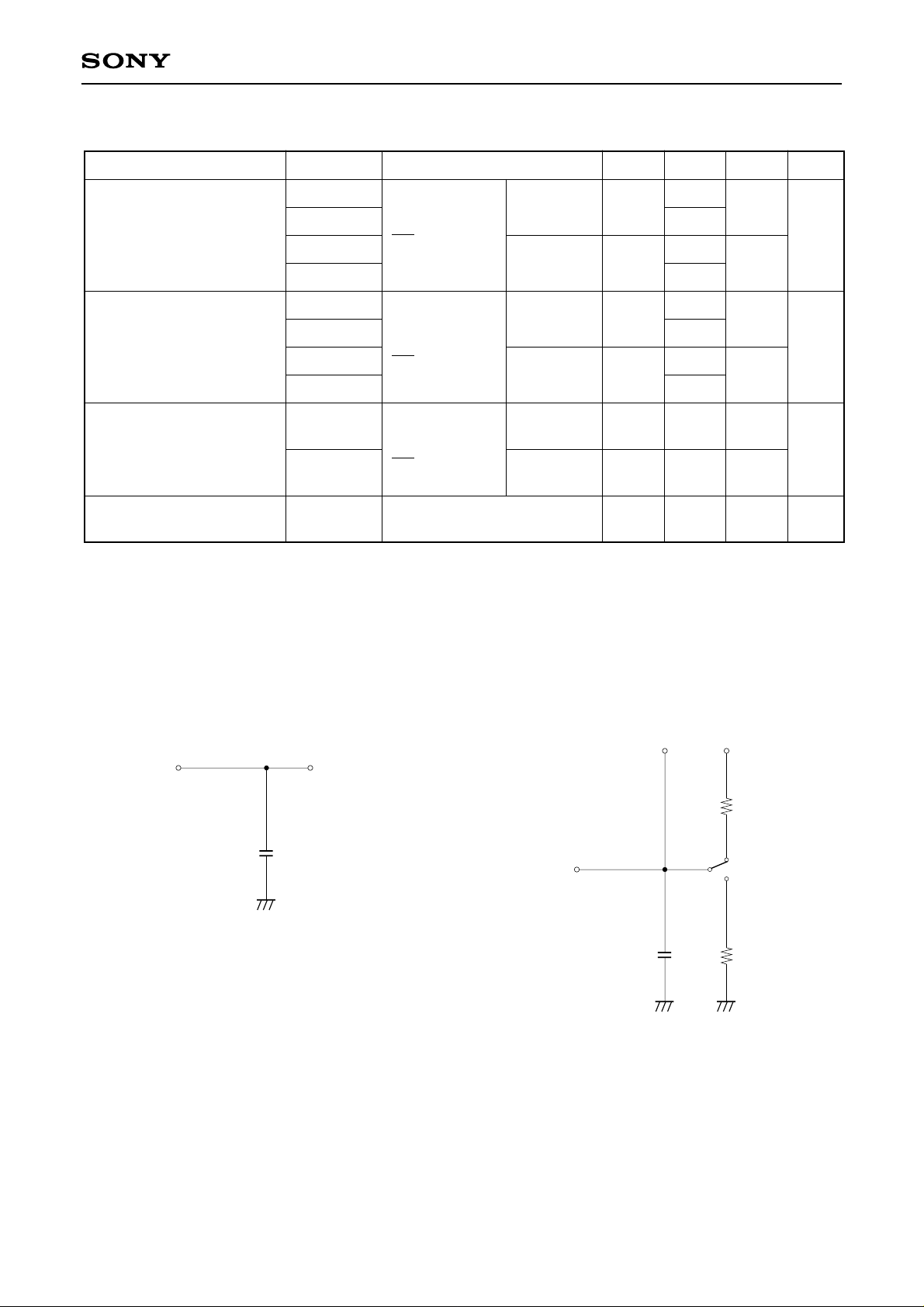
CXD2302Q
Timing
Item Symbol Conditions Min. Typ. Max. Unit
Output data delay
Tri-state
output enable time
Tri-state
output disable time
Clamp pulse width
∗
The clamp pulse width is for NTSC as an example. Adjust the rate to the clamp pulse cycle (1/15.75kHz for
NTSC) for other processing systems to equal the values for NTSC.
∗
(Fc = 50MHz, AVDD = 5V, DVDD = 5V or 3.3V, VRB = 0.5V, VRT = 2.5V, Ta = 25°C)
tpLH
tpHL
tpLH
tpHL
tpZH
tpZL
tpZH
tpZL
tpHZ
tpLZ
tpHZ
tpLZ
tCPW
DVDD = 5V
CL = 15pF
OE = 0V
DVDD = 3.3V
RL = 1kΩ
CL = 15pF
OE = 3V → 0V
RL = 1kΩ
CL = 15pF
OE = 0V → 3V
Fc = 14.3MHz, CIN = 10µF
for NTSC wave
DVDD = 5V
DVDD = 3.3V
DVDD = 5V
DVDD = 3.3V
5.5
4.3
2.5
3.0
3.5
2.5
1.75
9.5
8.5
11.8
7.6
4.5
6.0
7.0
5.0
5.5
5.5
2.75
12.0
16.3
8.0
9.0
7.5
8.0
3.75
ns
ns
ns
µs
Electrical Characteristics Measurement Circuit
Output data delay measurement circuit Tri-state output measurement circuit
Measurement point DVDD
To output pin
Note) CL includes capacitance of probes.
Measurement
point
CL
To output pin
CL RL
RL
– 8 –
 Loading...