

Sony CXD2301Q Datasheet

CXD2301Q
For the availability of this product, please contact the sales office.
8-bit 30MSPS Video A/D Converter with Built-in Amplifier/Clamp
Description
The CXD2301Q is an 8-bit CMOS A/D converter
for video applications with built-in amplifier/syncclamp circuits. A maximum conversion rate of
30MSPS is attained at a low power consumption by
adopting a 2-step parallel system.
Features
• Resolution: 8 bits ±1/2LSB (DL)
• Maximum sampling frequency: 30MSPS
• Low power consumption: 120mW (at 30MSPS
typ.)
(Including reference current)
• Standby function:
0.5mW power consumption in standby
• Amplifier functions:
provided
• Synchronous clamp function
• Clamp ON/OFF function
• Reference voltage self-bias circuit
• TTL compatible output
• 3V digital interface capability
• Single 5V or dual 4.75/3.3V power supplies
• Low input capacitance: 8pF
• Reference impedance: 330Ω (typ.)
Applications
Wide range of application fields where high-speed
A/D conversion is required such as in the digital
systems of TVs, VCRs, etc.
Structure
Silicon gate CMOS IC
Built-in 3x amplifier (15MHz band),
2-input selector function
Absolute Maximum Ratings (Ta = 25°C)
• Supply voltage VDD 7V
•Reference voltage VRT, VRB
• Input voltage (analog) VIN
• Input voltage (digital) VIH, VIL
• Output voltage (digital) VOH, VOL
• Storage temperature Tstg –55 to +150 °C
Recommended Operating Conditions
• Supply voltage IDVSS–AVSSI0 to 100 mV
Single power supply AVDD, DVDD5.0 ± 0.25 V
Dual power supply AVDD 4.75 ± 0.25 V
• Reference input voltage
• Analog input ADIN More than 1.2Vp-p
• Clock pulse width TPWI 16 (min) ns
• Operating ambient temperature
32 pin QFP (Plastic)
VDD +0.5 to VSS –0.5 V
VDD +0.5 to VSS –0.5 V
VDD +0.5 to VSS –0.5 V
VDD +0.5 to VSS –0.5 V
DVDD 3.3 ± 0.3 V
VRB 0 to V
VRT to 2.2 V
TPWO 16 (min) ns
Topr –20 to +75 °C
Sony reserves the right to change products and specifications without prior notice. This information does not convey any license by
any implication or otherwise under any patents or other right. Application circuits shown, if any, are typical examples illustrating the
operation of the devices. Sony cannot assume responsibility for any problems arising out of the use of these circuits.
– 1 –
E92Y50B4X-PK
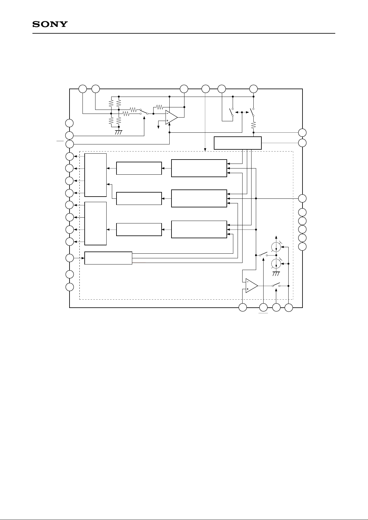
Block Diagram
27
25
30
21
22
CXD2301Q
AVDDADVADVOPOVIN2 VIN1
26
TEST
SS)
(DV
SEL
CE
D0(LSB)
D1
D2
D3
D4
D5
D6
D7(MSB)
CLK
DD
DV
DVSS
19
16
15
14
13
12
11
10
18
17
R
R
4
5
Lower
data
latch
Upper
data
latch
9
Clock generator
8
Lower encoder
(4 bit)
Lower encoder
(4 bit)
Upper encoder
(4 bit)
3R
VBI
A/D Converter
Lower
sampling comparator
(4 bit)
Lower
sampling comparator
(4 bit)
Upper
sampling comparator
(4 bit)
Block
Reference supply
RTS
ADV
23
29
28
31
VRT
VRB
1
ADIN
AVSS
2
AVSS
3
AVSS
7
AVSS
AVSS
24
VREF CLE CLP CCP
6
20
32
– 2 –
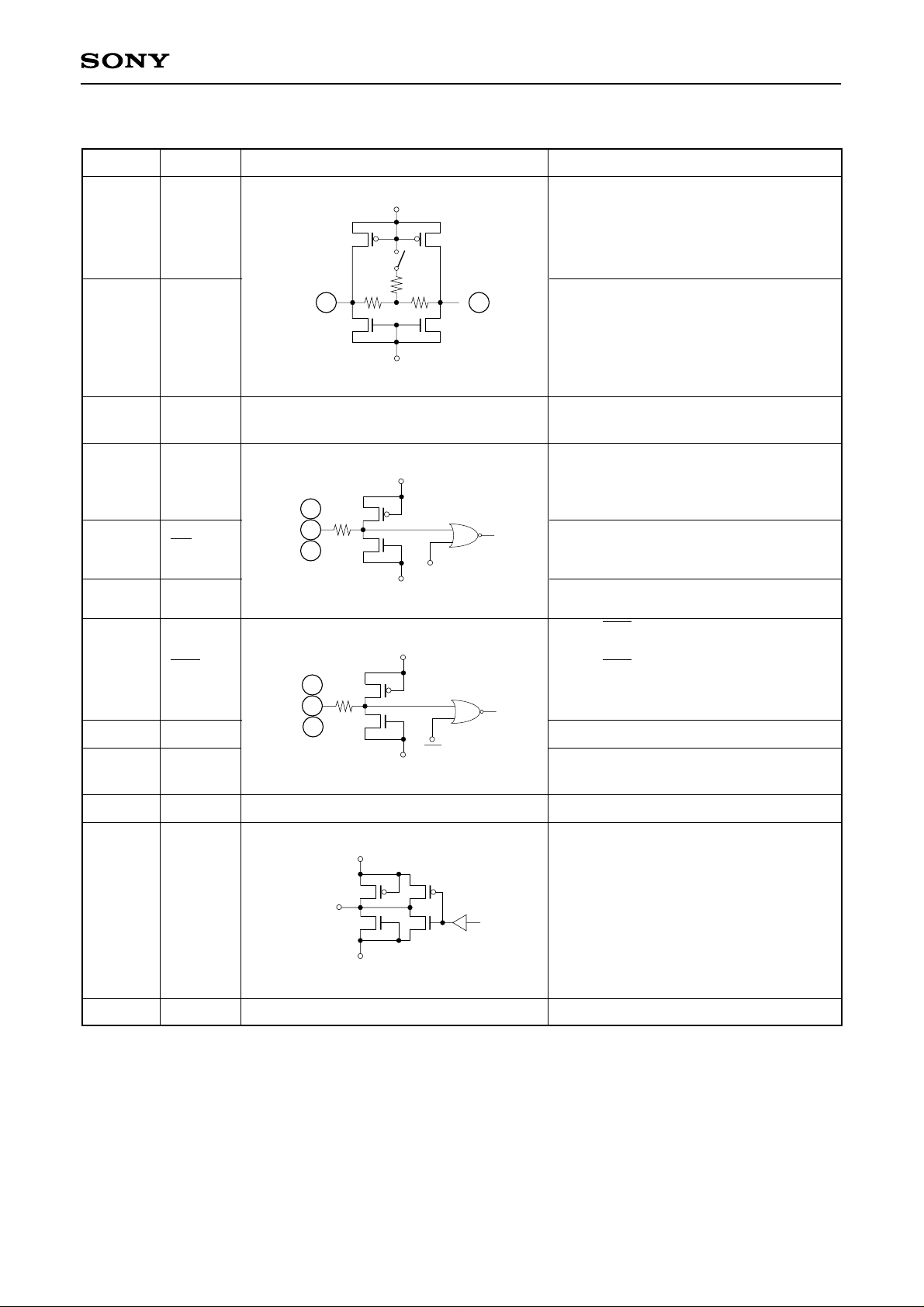
Pin Description
CXD2301Q
Pin No. Symbol
1VRB
23 VRT
2, 3, 7,
28, 31
AVSS
4 SEL
5CE
19 TEST
Equivalent circuit Description
AVDD
Reference voltage (bottom)
Connect to AVSS for normal use.
When another external voltage is input,
connect an external 0.1µF capacitor and
retain a 1.5V differential compared to the
top reference voltage.
Reference voltage (top)
By setting VRB to AVSS, outputs
23
TS
R
Rref
1
approximately 1.5V.
Connect only a 0.1µF external by-pass
capacitor for normal use.
AVSS
When another external voltage is input, it
must be 2.2V or lower.
Analog GND.
AVDD
4
5
19
DVSS
AVSS
Switches the input of the 3x amplifier.
When SEL is at Low level, VIN1 is selected.
When SEL is at High level, VIN2 is selected.
Standby function ON/OFF selector.
In standby state when High.
Fix to VSS for normal use.
6 CLE
18 CLK
20 CLP
8DVSS
9 to 16 D7 to D0
17 DVDD
20
18
AVDD
enabled.
When CLE = High: Clamp function is
When CLE = Low: Clamp functiion is
6
disabled, and only the normal A/D
converter function is enabled.
Clock input
CE
AVSS
Inputs the clamp pulse to Pin 20 (CLP).
Clamps the High interval signal voltage.
Digital GND.
D7 (MSB) to D0 (LSB) output
Outputs Low level in standby.
Di
In operation, the phase of D7 to D0
output is inverted against the phase of
ADIN.
5V or 3.3V
– 3 –
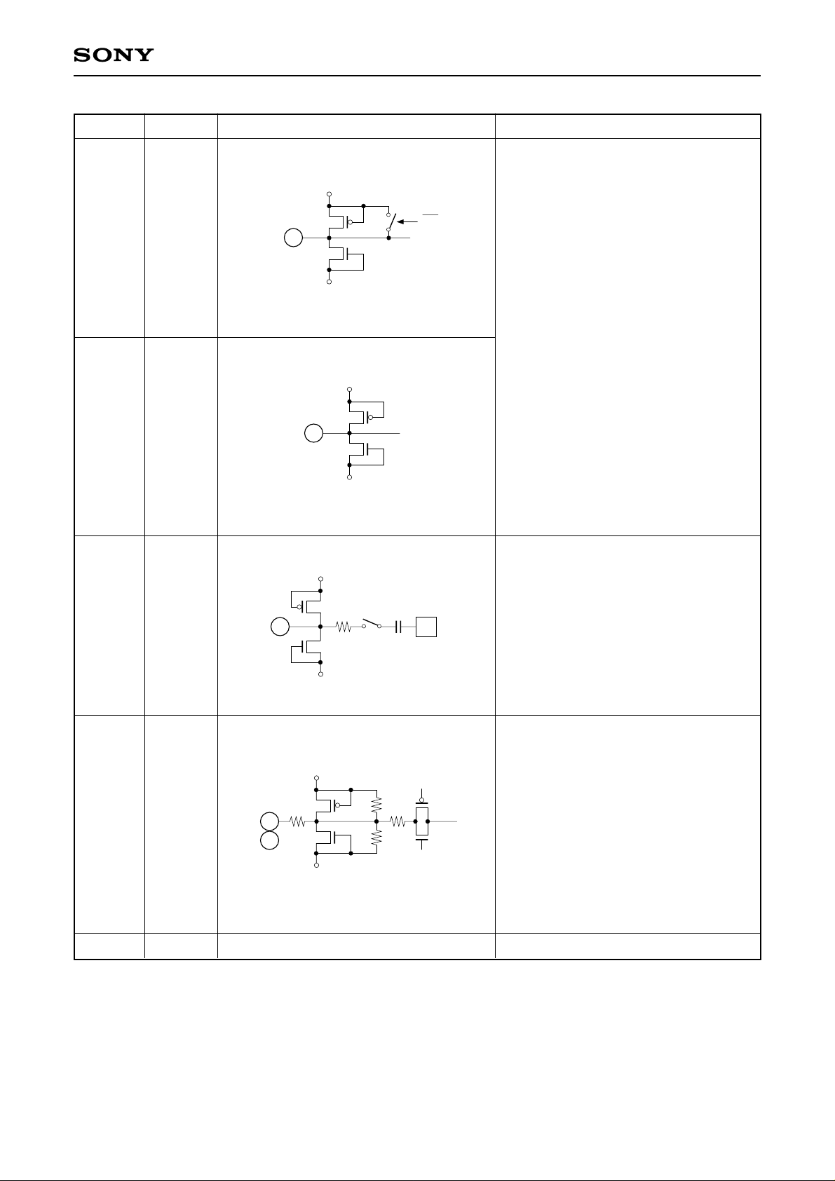
Pin No. Symbol Equivalent circuit Description
AVDD
CE
21 ADV
21
AVSS
Short Pins 21 and 22, and connect 0.1µF
external capacitor.
AVDD
CXD2301Q
22 ADV
24 VREF
25
27
VIN1
VIN2
22
AVSS
AVDD
24
AVSS
AVDD
200 R
25
27
AVSS
R11
R12
Clamp reference voltage input.
Clamps so that the reference voltage
and the clamp interval ADIN input signal
are equal.
The reference voltage is more than 0.5V.
Amplifier input pin.
Biased internally
at 1.9V (when AVDD = 5V) or
at 1.8V (when AVDD = 4.75V).
When in standby as well.
When SEL is at Low level, VIN1 is
selected for input;
When SEL is at High level, VIN2 is
selected for input.
26 AVDD
5V or 4.75V
– 4 –
Pin No. Symbol Equivalent circuit Description
AVDD
CXD2301Q
29 ADIN
30 OPO
32
CCP
29
32
30
A/D converter block analog input.
AVSS
AVDD
Amplifier output.
The phase of this output is inverted
against the phase of VIN1, 2.
In standby mode, it becomes
high-impedance output condition.
AVSS
AVDD
Integrates the clamp control voltage.
The relationship between the CCP
voltage variation and the ADIN voltage
is positive phase.
AVSS
• The following table shows the status of the digital output pins when the TEST pin is used with the CE and
SEL pins.
TEST
L
L
H
H
H
CE
L
H
L
H
H
SEL
X
X
X
L
H
D1 D2 D3 D4 D5 D6 D7 D8
D1 D2 D3 D4 D5 D6 D7 D8
LLLLLLLL
TEST mode
HLHLHLHL
LHLHLHLH
– 5 –
CXD2301Q
Digital Output
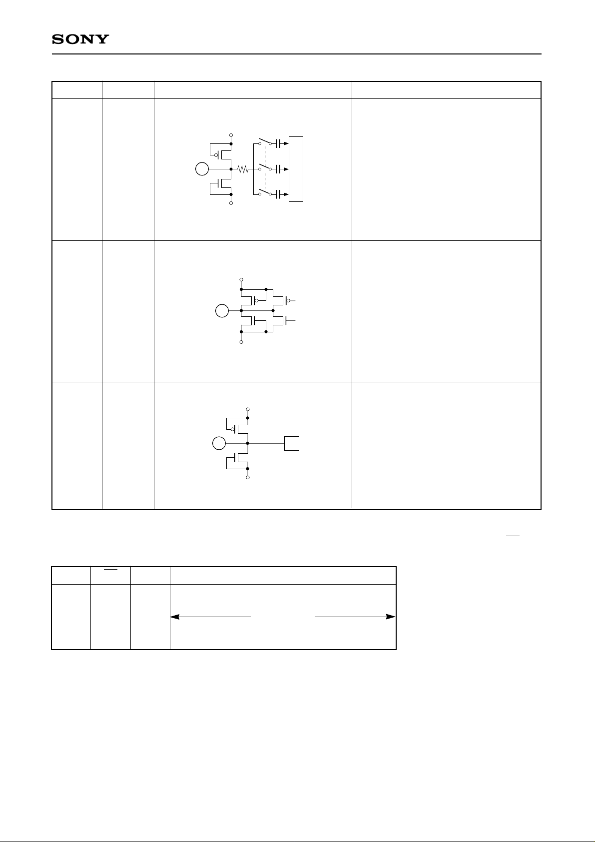
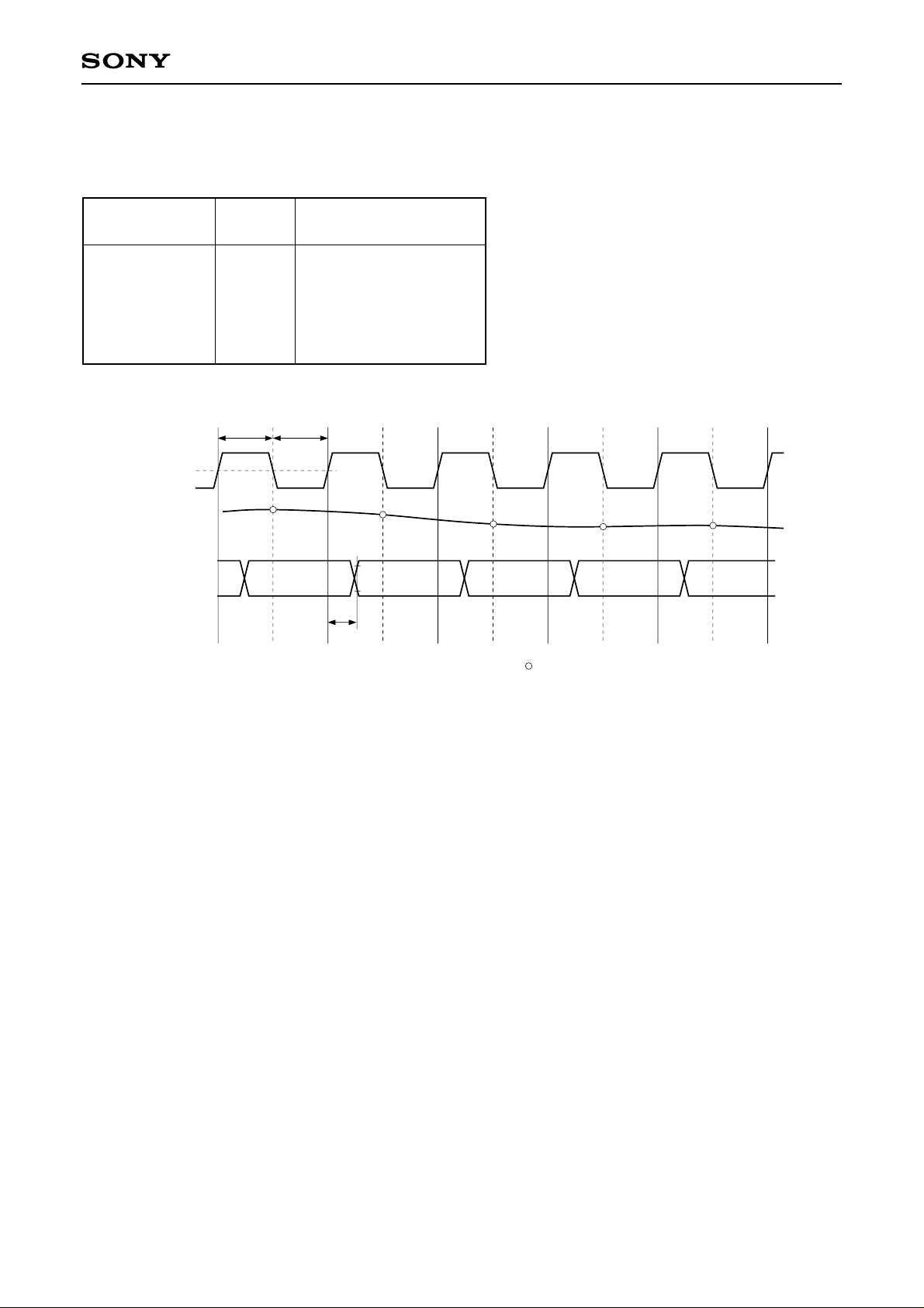
The following table shows the correlation between the ADIN input voltage and the digital output code.
Take notice that the phase of ADIN input signal voltage is inverted against the phase of the digital output.
ADIN
Input signal voltage
VRT
:
:
:
:
VRB
Clock 2V
ADIN input
Data output
Step
MSB LSB
0
:
127
128
:
255
TPW1 TPW0
N
N–3 N–2 N+1 N N–1
Digital output code
0 0 0 0 0 0 0 0
:
0 1 1 1 1 1 1 1
1 0 0 0 0 0 0 0
:
1 1 1 1 1 1 1 1
N+1
Td
N+2
N+3
N+4
Fig. 1. Timing Chart
: Indicates point at which input signal is sampled
– 6 –
CXD2301Q
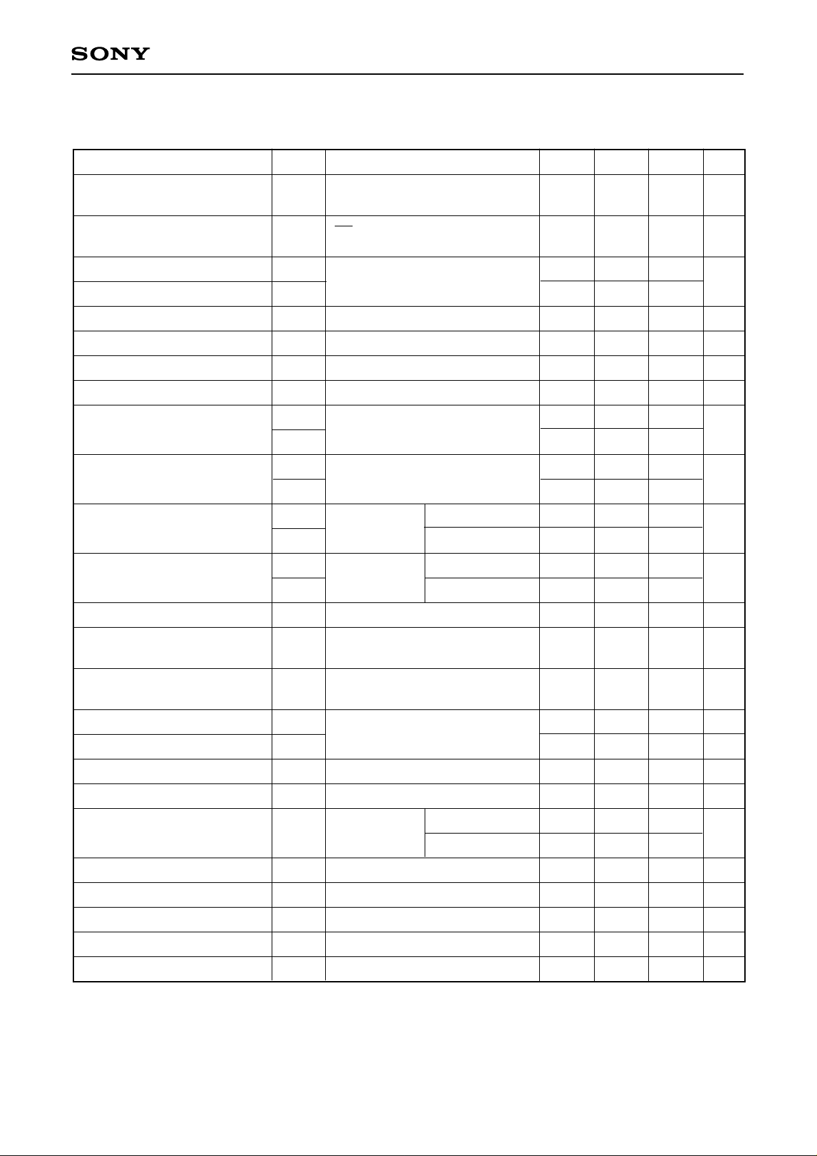
Electrical Characteristics
(1) When using a single power supply (Fc = 30MSPS, AVDD = DVDD = +5V, VRB = 0V, VRT = 1.5V, Ta = 25°C)
Item Symbol Conditions Min. Typ. Max. Unit
Supply current
Standby supply current
Max. conversion rate
Min. conversion rate
ADIN input band (at –1dB)
ADIN input capacitance
Reference resistance (VRT to VRB)
Self bias
Offset voltage
Digital input voltage
Digital input current
Digital output current
IAD +
IDD
ISTB
Fc max
Fc min
BW
CADIN
RREF
VRT
EOT
EOB
VIH
VIL
IIH
IIL
IOH
IOL
Fc = 35MSPS
NTSC ramp wave input
CE = DVDD
VIN = 0 to 1.5V
fIN = 1kHz ramp
VIN = 0.75V + 0.07Vrms
VRB = AVSS
VIH = VDD
DVDD = max.
VIL = 0V
VOH = VDD–0.5V
DVDD = min.
VOL = 0.4V
30
230
1.38
–40
+25
3.5
–1.1
3.7
27
130
20
8
330
1.52
–20
+45
–2.5
6.5
35
200
0.5
440
1.66
0
+65
0.5
5
5
mA
µA
MSPS
MHz
pF
Ω
V
mV
V
µA
mA
Output data delay
Integral nonlinearity error
Differential nonlinearity error
Differential gain error
Differential phase error
Aperture jitter
Sampling delay
Clamp offset voltage
Clamp pulse delay
Amplifier gain
VIN1 and VIN2 bias voltage
VIN1 and VIN2 input resistance
VIN1 and VIN2 input capacitance
TDL
EL
ED
DG
DP
taj
tsd
Eoc
tcpd
VBI1, 2
RI1, 2
CI1, 2
With TTL 1gate and 10pF load
Fc = 30MSPS
VIN = 0 to 1.5V
Fc = 30MSPS
VIN = 0 to 1.5V
NTSC 40IRE mod
ramp, Fc = 14.3MSPS
VADIN = DC,
PWS = 3µsec
VREF = 0.5V
VREF = 1.5V
DC to 15MHz
When open
7
0
–40
8.5
19
13
+0.5
±0.3
1
0.5
30
2
+20
–20
25
9.5
1.9
27
15
25
+1.3
±0.5
+40
0
10.5
35
ns
LSB
LSB
%
deg
ps
ns
mV
ns
dB
V
kΩ
pF
– 7 –
 Loading...