

Sony CXD2053AS, CXD2053AM Datasheet
CXD2053AM/AS
For the availability of this product, please contact the sales office.
Auto Wide, EDTV-II ID Detection, ID-1 Detection
Description
The CXD2053AM/AS is an IC which has the three
functions of identifying the wide video (auto wide),
detecting the EDTV-II ID, and detecting ID-1 (EIAJ,
CPX1024) from the video signal.
Features
• Video aspect ratio identification used with wide
TVs is realized with a single chip.
• I2C bus interface.
This IC can also be used without the bus.
• For auto wide function, 525/60 (NTSC) and 625/50
(PAL, SECAM) can be Supported.
Applications
Wide TV
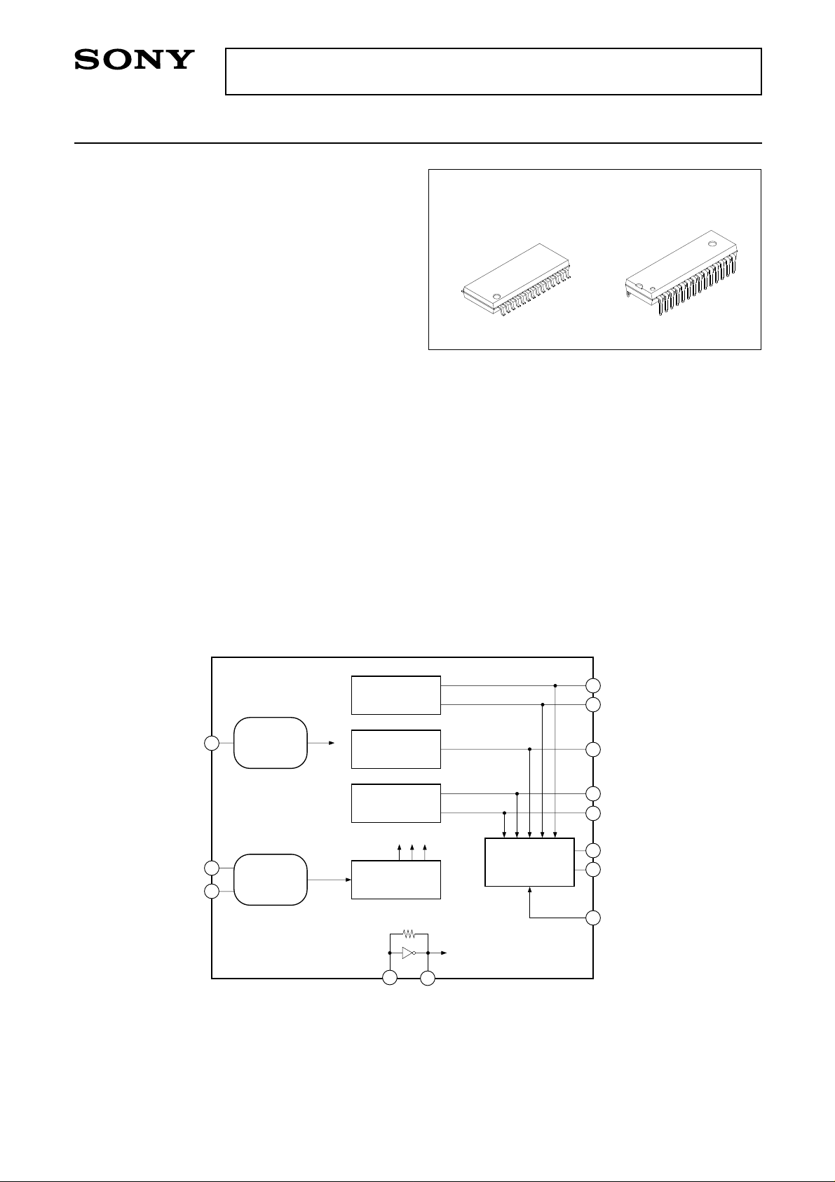
Structure
Silicon gate CMOS IC
CXD2053AM
28 pin SOP (Plastic)
CXD2053AS
28 pin SDIP (Plastic)
Absolute Maximum Ratings
• Supply voltage VDD VSS – 0.5 to +7.0 V
• Input voltage VI VSS – 0.5 to VDD + 0.5 V
• Output voltage VO VSS – 0.5 to VDD + 0.5 V
• Storage temperature
Tstg –55 to +150 °C
Recommended Operating Conditions
• Supply voltage VDD 4.5 to 5.5 V
• Operating temperature
Topr –20 to +70 °C
Block Diagram
ADIN
VDIN
VSIN
2
11
10
AD Converter
Data Slice Sync
Separator
Auto wide
Identification
EDTV-II
ID Decoder
ID-1 Decoder
Timing Signal
Generator
22
XI
26
OAW1
27
OAW2
OED
28
25
O164
24
OLBX
SCL
I2C Bus Interface
21
XO
15
16
SDA
19
MCON
Sony reserves the right to change products and specifications without prior notice. This information does not convey any license by
any implication or otherwise under any patents or other right. Application circuits shown, if any, are typical examples illustrating the
operation of the devices. Sony cannot assume responsibility for any problems arising out of the use of these circuits.
– 1 –
E96531-ST
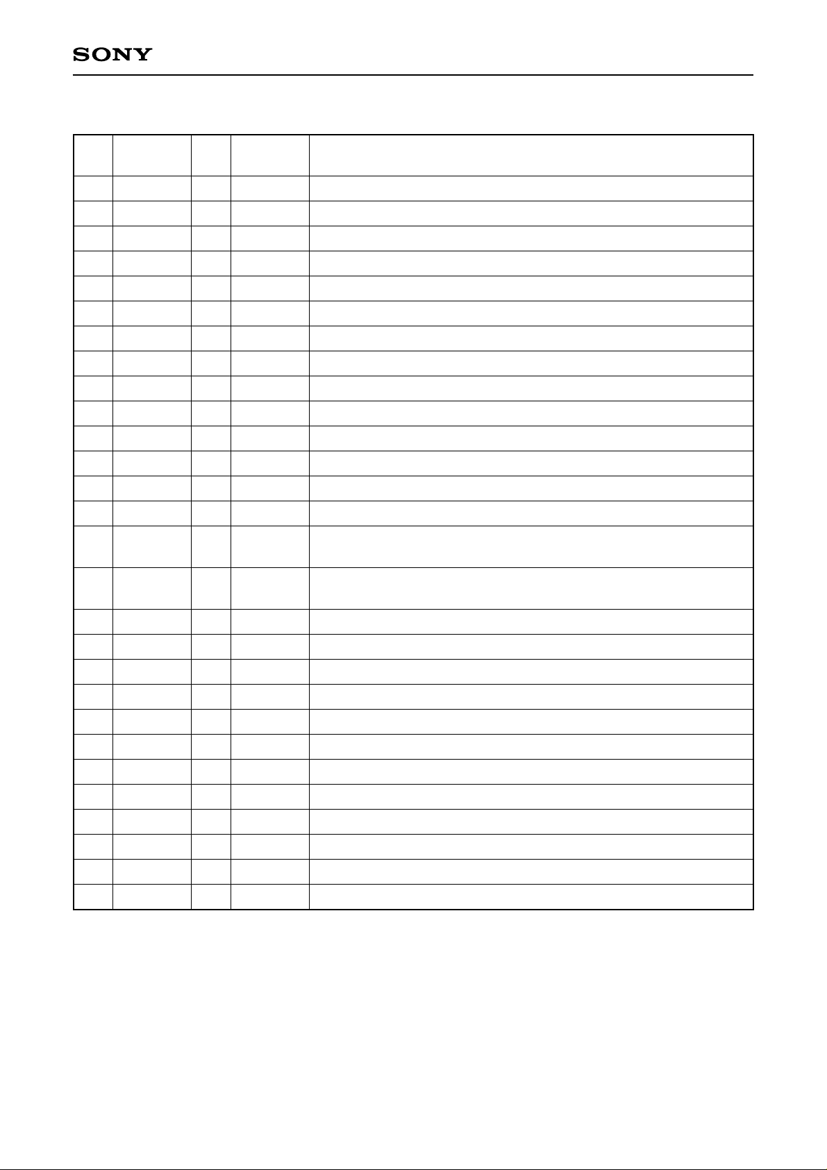
Pin Description
CXD2053AM/AS
Pin
No.
1
2
3
4
5
6
7
8
9
10
11
12
13
14
15
Symbol I/O I/O level Description
AVDD
ADIN
AVSS
CPV
VRB
VRT
CCP
ISET
AVDD
VSIN
VDIN
AVSS
TST1
TST2
SCL
[EDDEC2]
I
I
I
I
I
I
I
I
I
I
I
ANALOG
ANALOG
ANALOG
ANALOG
ANALOG
ANALOG
ANALOG
ANALOG
ANALOG
ANALOG
∗
2
TTL
∗
2
TTL
CMOS
∗1
Analog power supply.
AD converter input.
Analog ground.
Clamp voltage.
AD converter bottom voltage.
AD converter top voltage.
AD converter clamp integrating capacitor connection.
Bias current setting.
Analog power supply
Sync separation input.
Data slicer input.
Analog ground.
Test input; connect to VSS.
Test input; connect to VSS.
I2C bus clock [EDTV-II decoding identification switching]
SDA
16
[ED2FSC]
17
VSS
18
XRST
19
MCON
20
VDD
21
XO
22
XI
23
VSS
24
OLBX
25
O164
26
OAW1
27
OAW2
28
OED
∗1
Schmitt input
∗2
With pull-down resistor
∗3
Open drain
I/O
I
I
O
I
O
O
O
O
O
CMOS
TTL
TTL
CMOS
CMOS
CMOS
CMOS
CMOS
CMOS
CMOS
∗1, 3
I2C bus data [EDTV-II 3.58 M check existence]
Digital ground.
∗
1
Reset at 0.
I2C bus-free mode switching; 0 = I2C-free.
Digital system power supply.
Oscillator connection (14.318MHz).
Oscillator connection or clock input.
Digital ground.
VB-ID detection output; 1 = letter-box, 0 = normal.
VB-ID detection output; 1 = full mode.
Auto wide identification output; 1 = wide video subtitles not present.
Auto wide identification output; 1 = wide video subtitles present.
EDTV-II ID bit 3 detection output.
Note) In I2C-free mode when Pin 19 (MCON) = 0, Pins 15 and 16 switch to the functions in parentheses [ ].
– 2 –
CXD2053AM/AS
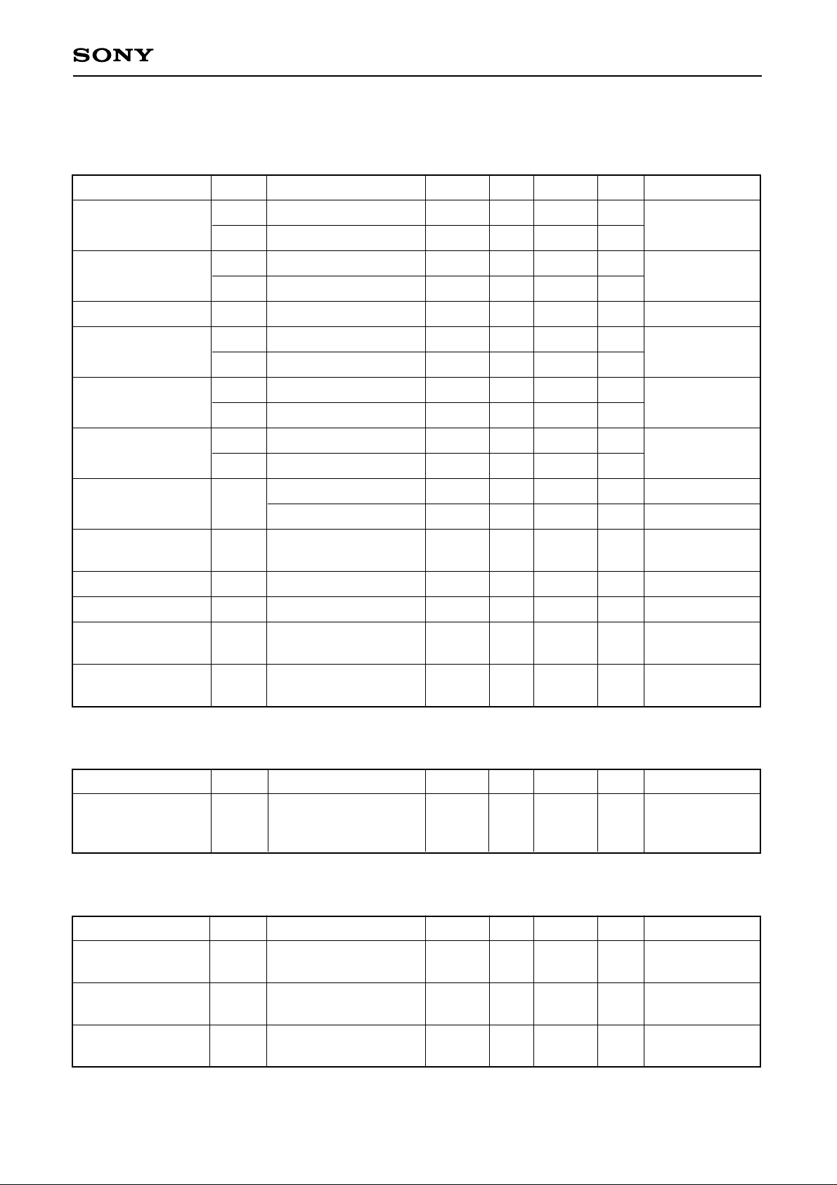
Electrical Characteristics
DC Characteristics (Logic Section) (VDD = 5.0V, VSS = 0V, Ta = 25°C)
Item
Output voltage
Output voltage
Output voltage
Input voltage
Input voltage
Input voltage
Input hysteresis
width
Input leak current
Output leak current
Symbol Condition Min. Typ. Max. Unit Remarks
VOH
VOL
VOH
IOH = –2mA
IOL = 4mA
IOH = –3mA
VDD – 0.8
VDD/2
0.4
V
Pins 24, 25, 26,
27 and 28
V
V
Pin 21 only
VOL
VOL
VIH
VIL
VIH
IOL = 3mA
IOL = 3mA
2.2
0.7 × VDD
VDD/2
0.4
0.8
V
V
Pin 16 only
V
Pins 13, 14, 18
and 19
V
V
Pin 22 only
VIL
VIH
0.8 × VDD
0.3 × VDD
V
V
Pins 15 and 16
VIL
0.05 ×VDD
0.2 × VDD
V
V
Pins 15 and 16
Vhys
Ii
IOZ
VIN = either VSS or VDD
VIN = eother VSS or VDD
–10
–40
0.4
+10
+40
V
Pin 18
Except for Pins
µA
13, 14 and 22
µA
Pin 16 only
Input current
Feedback resistor
Current consumption
Ii
Rfbk
IDD
VIN = VDD
XI (Pin 22) = either
VDD or VSS
Clock 14.318MHz
40
250k
100
1M
29
240
2.5M
µA
Ω
mA
Pins 13 and 14
Between Pins 21
and 22
Sum of Pins 1, 9
and 20
AC Characteristics (VDD = 5.0V, VSS = 0V, Ta = 25°C)
Item
Symbol Condition Min. Typ. Max. Unit Remarks
Pin 22 input, or
Clock frequency fxi
14.318
MHz
oscillator between
Pins 21 and 22
I/O Pin Capacitance
Item
Input pin
capacitance
Output pin
capacitance
Symbol Condition Min. Typ. Max. Unit Remarks
CIN
COUT
VDD = VI = 0V,
f = 1MHz
VDD = VI = 0V,
f = 1MHz
9
11
pF
pF
Input/output pin
capacitance
CI/O
VDD = VI = 0V,
f = 1MHz
– 3 –
11
pF
CXD2053AM/AS
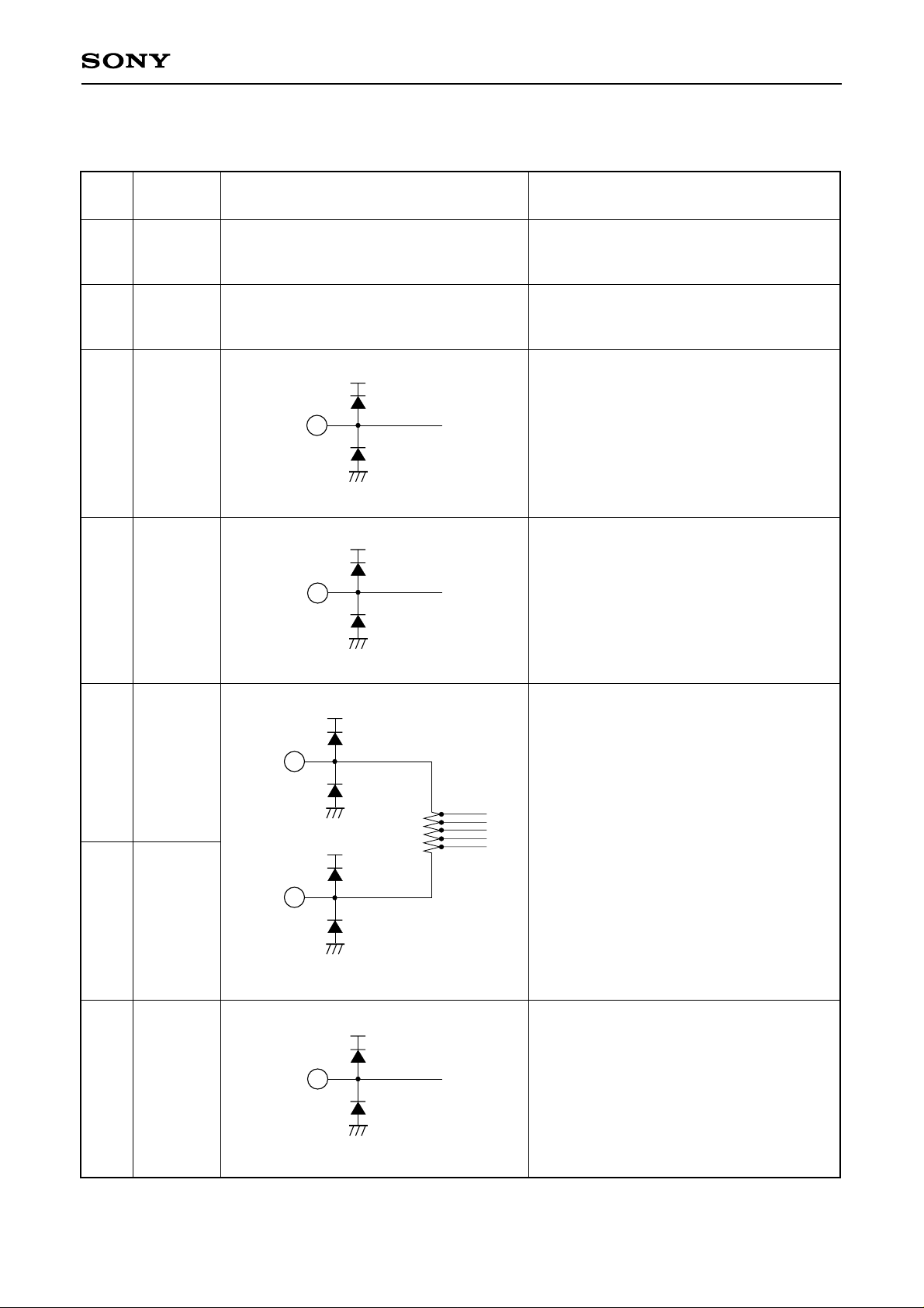
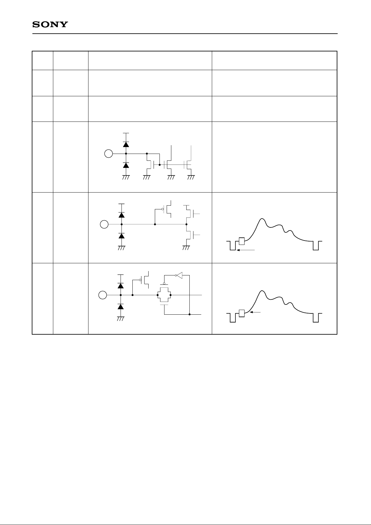
Pins and Electrical Characteristics
Analog Section (VDD = 5.0V, VSS = 0V, Ta = 25°C)
Pin
No.
1
3
2
4
Symbol Equivalent circuit Description
AD converter analog power supply.
Connect a low-noise power supply from the
digital system.
AD converter analog ground.
Connect to the same potential as other VSS
and AVSS.
AVDD
AVSS
Not connected to VDD (Pin 20) or AVDD
(Pin 9) inside the IC.
Not connected to VSS (Pins 17 and 23) or
AVSS (Pin 12) inside the IC.
AVDD
AD converter input.
ADIN
2
This pin is pedestal clamped to the
potential of CPV (Pin 4), so input the video
signal with capacitor coupled.
AVSS
AVDD
CPV
4
ADIN (Pin 2) pedestal clamp voltage
setting.
AVSS
AVDD
5
VRB
6
AVSS
AVDD
AD converter input range setting.
The resistor between Pins 5 and 6 is 310Ω
(Typ.).
5
6
VRT
AVSS
AVDD
7
CCP
7
Clamp circuit integrating capacitor
connection. Connect 0.022µF between this
pin and AVSS (Pin 3).
AVSS
– 4 –
CXD2053AM/AS
Pin
No.
9
12
8
10
Symbol Equivalent circuit Description
Sync separation system analog power supply.
Connect a low-noise power supply from the
digital system.
Sync separation system analog ground.
Connect to the same potential as other VSS
and AVSS.
Bias setting.
Connect to AVDD (Pin 9) with 33kΩ.
Chip clamp, sync separation input.
AVDD
AVSS
ISET
Not connected to VDD (Pin 20) or AVDD
(Pin 1) inside the IC.
Not connected to AVSS (Pin 3) or VSS
(Pins 17 and 23) inside the IC.
AVDD
8
AVSS
AVDD
Input with capacitor coupled.
VSIN
10
11
VDIN
11
AVSS
AVDD
AVSS
Clamp voltage 1.5V
Pedestal clamp, ID-1 data slicer input.
Input with capacitor coupled.
Clamp voltage
1.5V
– 5 –
 Loading...