

Sony CXD2044Q Datasheet
CXD2044Q
For the availability of this product, please contact the sales office.
Digital Comb Filter (NTSC/PAL/PAL-M/PAL-N)
Description
The CXD2044Q is an adaptive intra-field comb
filter compatible with NTSC, PAL, PAL-M and PAL-N
systems, and can provide high-precision Y/C
separation with a single chip.
Features
• Intra-field Y/C separation by adaptive processing
• 8-bit A/D converter (1-channel)
• 8-bit D/A converter (2-channel)
• Four 1H delay lines
• Clock 4fsc
Absolute Maximum Ratings (Ta = 25°C, Vss = 0V)
• Supply voltage DVDD VSS – 0.5 to +7.0 V
AAVD VSS – 0.5 to +7.0 V
ADVD VSS – 0.5 to +7.0 V
YVDD VSS – 0.5 to +7.0 V
CVDD VSS – 0.5 to +7.0 V
• Input voltage VI VSS – 0.5 to VDD + 0.5 V
• Output voltage VO VSS – 0.5 to VDD + 0.5 V
• Storage temperature
Tstg –55 to +150 °C
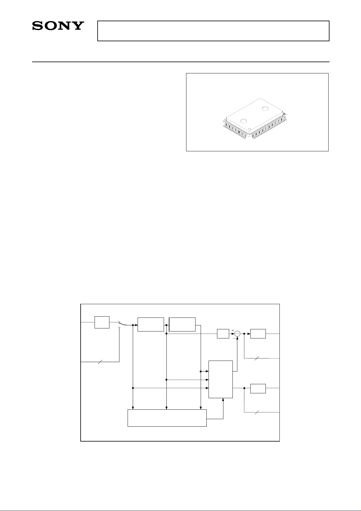
Block Diagram
Recommended Operating Conditions
• Supply voltage DVDD 5.0 ± 0.25 V
• Analog input ADIN 1.8 Vp-p
• Operating temperature
Applications
Y/C separation for color TVs and VCRs
Structure
Silicon gate CMOS IC
80 pin QFP (Plastic)
AAVD 5.0 ±0.25 V
ADVD 5.0 ± 0.25 V
YVDD 5.0 ± 0.25 V
CVDD 5.0 ± 0.25 V
Topr –20 to +75 °C
Analog Vin
Digital Vin
Sony reserves the right to change products and specifications without prior notice. This information does not convey any license by
any implication or otherwise under any patents or other right. Application circuits shown, if any, are typical examples illustrating the
operation of the devices. Sony cannot assume responsibility for any problems arising out of the use of these circuits.
A/D
8
NTSC: 1H
PAL: 2H
Logic operation
NTSC: 1H
PAL: 2H
– 1 –
DL D/A
Adaptive
filter
operation
8
D/A
8
A-Yout
D-Yout
A-Cout
D-Cout
E95418-ST
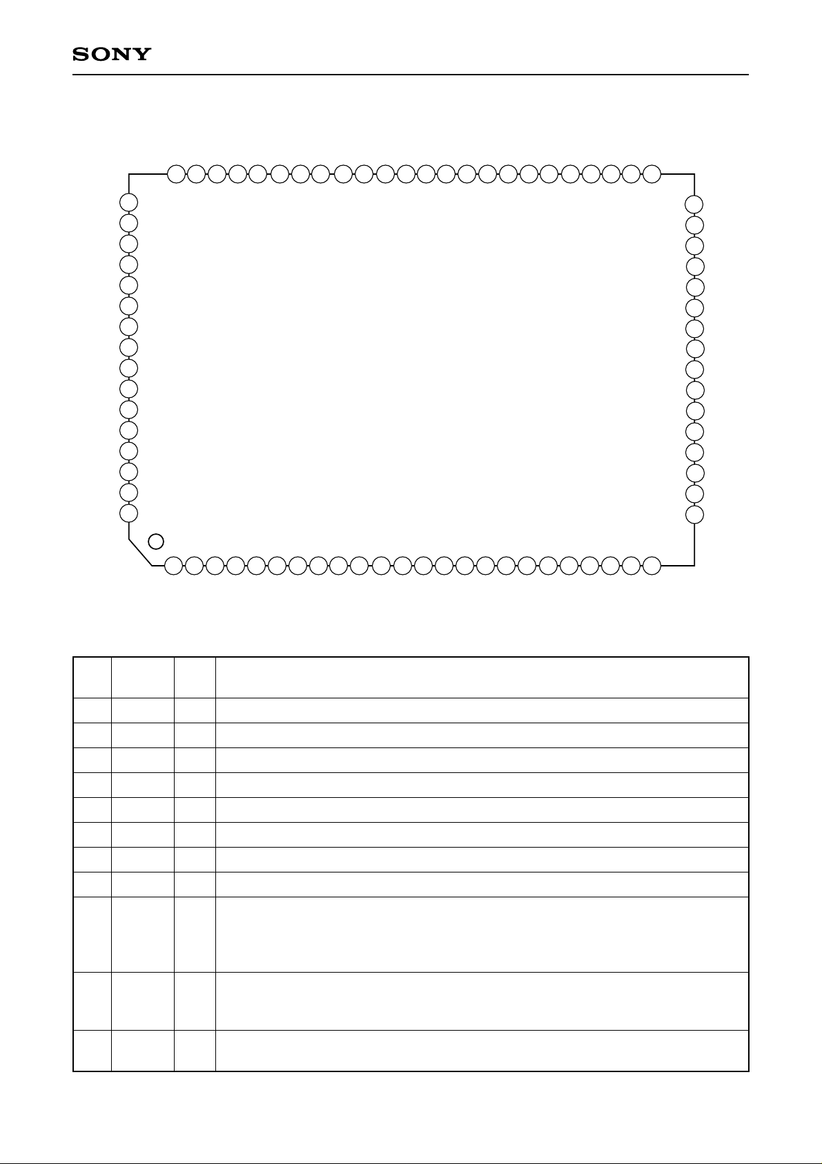
Pin Configuration
64
TEST
65
TEST
66
XCOE
67
APCN
68
RATI
69
NTPL
70
YOT
71
DVss
72
DV
DD
73
DTR
74
TEST
75
PMN
76
TEST
77
TEST
78
BPF
79
TEST
80
C1
63
C2
62
C3
61
C4
60
C5
59
C6
58
C7
57
C8
XYOE
56
CONT
55
54
TEST
53
DD
DV
52
DVss
51
Y1
50
Y2
49
Y3
48
Y4
47
Y5
46
Y6
45
Y7
44
Y8
43
CVss
42
CIRF
41
CVRF
CXD2044Q
40
CVG
39
ACO
38
XACO
37
CVDD
36
VB
35
YVss
34
YIRF
33
YVRF
32
YVG
31
AYO
30
XAYO
29
YVDD
28
ADVD
27
RT
26
AAVD
25
ADIN
Pin Description
Pin
Symbol
No.
1
VI8
2
VI7
3
VI6
4
VI5
5
VI4
6
VI3
7
VI2
8
VI1
9
ADCO
6
VI6
5
4
VI3
VI4
VI5
1
2
3
VI7
VI8
9
10
8
7
VI1
VI2
INSL
ADCO
11
12
OCLK
13
DVss
14 15
DD
DV
CLKO
MCK
I/O Description
I
Digital input (MSB). Connect to DVDD or DVss when not in use.
I
Digital input. Connect to DVDD or DVss when not in use.
I
Digital input. Connect to DVDD or DVss when not in use.
I
Digital input. Connect to DVDD or DVss when not in use.
I
Digital input. Connect to DVDD or DVss when not in use.
I
Digital input. Connect to DVDD or DVss when not in use.
I
Digital input. Connect to DVDD or DVss when not in use.
I
Digital input (LSB). Connect to DVDD or DVss when not in use.
A/D converter output through mode.
High: Video signals taken into the A/D converter (input pin: ADIN) are output without
I
change from the Y output pins as 8-bit digital data with a 3.5 clock delay.
Low: Standard mode
16
17
ADCK
18
CLPI
19
ADVS
XCPON
20
ICP
21
22
CRV
RB
23
24
GR
AAVS
10
11
INSL
OCLK
Input switching. Switches the input data fed to the comb filter.
I
High: Digital input
Low: Analog input
Clock amplifier input.
I
Input 0.8Vp-p or more, eliminating the DC components with a capacitor.
– 2 –
Pin
Symbol I/O Description
No.
12
13
14
DVSS
DVDD
CLKO
—
Digital ground.
—
Digital power supply. (5V)
O
Clock amplifier output.
Master clock input.
15
MCK
I
Input the 4fsc clock locked to the color burst.
Normally, connect the clock amplifier output (CLKO: Pin 14).
Clock input for the A/D converter.
16
ADCK
I
Input the same clock as the master clock (MCK: Pin 15).
Normally, connect the clock amplifier output (CLKO: Pin 14).
Clamp pulse input for the A/D converter.
17
CLPI
I
Clamps the signal voltage during the low period of the clamp pulse signal.
When the clamp function is off, connect to the digital power supply (DVDD).
Clamp setting for the A/D converter.
18
XCPON
I
High: Clamp function is set to off, and the normal A/D converter function is only enabled.
Low: Clamp function is enabled.
CXD2044Q
19
20
21
22
23
24
25
26
27
28
29
30
31
ADVS
ICP
CRV
RB
GR
AAVS
ADIN
AAVD
RT
ADVD
YVDD
XAYO
AYO
—
Digital ground for the A/D converter.
Clamp control voltage integral pin.
I
Connect a capacitor of approximately 0.01µF.
When not using clamp, connect to the analog ground (AAVS).
Clamp reference voltage input.
I
Operates to make the analog input voltage equal to the clamp reference voltage during
the clamp period. When not using clamp, connect to the analog ground (AAVS).
O
Reference voltage (bottom): 0.5V (typ.)
—
Guard ring. Connect to the analog ground (AAVS).
—
Analog ground for the A/D converter.
I
Comb filter analog input (A/D converter input).
—
Analog power supply for the A/D converter. (5V)
O
Reference voltage (top): 2.6V (typ.)
—
Digital power supply for the A/D converter. (5V)
—
Analog power supply for the Y D/A converter. (5V)
AYO inverted current output.
O
Connect to the analog ground (YVss).
Analog luminance signal output.
O
Output can be obtained by connecting a resistor between this pin and the analog ground.
32
33
34
35
36
37
38
YVG
YVRF
YIRF
YVss
VB
CVDD
XACO
O
Connect a capacitor of approximately 0.1µF.
I
Sets the full-scale value of the analog luminance output signal.
O
Connect a resistor of “16R” (16 times the output resistor “R” of the AYO pin).
—
Analog ground for the Y D/A converter.
O
Connect a capacitor of approximately 0.1µF.
—
Analog power supply for the C D/A converter. (5V)
ACO inverted current output.
O
Connect to the analog ground (CVss).
– 3 –
Pin
No.
Symbol
CXD2044Q
I/O Description
39
40
41
42
43
44
45
46
47
48
49
50
51
52
53
54
ACO
CVG
CVRF
CIRF
CVss
Y8
Y7
Y6
Y5
Y4
Y3
Y2
Y1
DVss
DVDD
TEST
Analog chroma signal output.
O
Output can be obtained by connecting a resistor between this pin and the analog ground.
O
Connect a capacitor of approximately 0.1µF.
I
Sets the full-scale value of the analog chroma output signal.
O
Connect a resistor of “16R” (16 times the output resistor “R” of the ACO pin).
—
Analog ground for the C D/A converter.
O
Digital luminance signal output (MSB).
O
Digital luminance signal output.
O
Digital luminance signal output.
O
Digital luminance signal output.
O
Digital luminance signal output.
O
Digital luminance signal output.
O
Digital luminance signal output.
O
Digital luminance signal output (LSB).
—
Digital ground.
—
Digital power supply. (5V)
I
Test. Normally open or fix to “Low”.
55
56
57
58
59
60
61
62
63
64
65
66
67
CONT
XYOE
C8
C7
C6
C5
C4
C3
C2
C1
TEST
TEST
XCOE
I
Normally open or fix to “High”.
Digital luminance signal output control.
High: High impedance
I
Low: Standard output
However, during PAL-M/N mode (Pins 70 and 76 are both “High”), the digital chroma
signal output is also controlled simultaneously. See Table 1.
O
Digital chroma signal output (MSB).
O
Digital chroma signal output.
O
Digital chroma signal output.
O
Digital chroma signal output.
O
Digital chroma signal output.
O
Digital chroma signal output.
O
Digital chroma signal output.
O
Digital chroma signal output (LSB).
I
Test. Normally open or fix to “Low”.
I
Test. Normally open or fix to “Low”.
Digital chroma signal output control. See Table 1.
I
High: High impedance
Low: Standard output
68
APCN
Aperture compensation circuit setting.
High: Compensates for the aperture-induced frequency response characteristics degradation.
I
Even in through mode (YOT: H), aperture compensation is performed for the Y output.
Low: Standard mode
– 4 –
 Loading...