

Sony CXD2043Q Datasheet
Description
The CXD2043Q is an adaptive comb filter compatible
with NTSC system, and can provide high-precision Y/C
separation with a single-chip.
Features
• Y/C separation by adaptive processing
• Horizontal aperture compensation circuit
• 8-bit A/D converter (1-channel)
• 8-bit D/A converter (2-channel)
• Two 1H delay lines
• 4-PLL
Absolute Maximum Ratings (Ta = 25°C, Vss = 0V)
• Supply voltage DVDD VSS – 0.5 to +7.0 V
YVDD VSS – 0.5 to +7.0 V
CVDD VSS – 0.5 to +7.0 V
PVDD VSS – 0.5 to +7.0 V
• Input voltage VI VSS – 0.5 to VDD + 0.5 V
• Output voltage VO VSS – 0.5 to VDD + 0.5 V
• Operating temperature
Topr –20 to +75 °C
• Storage temperature
Tstg –55 to +150 °C
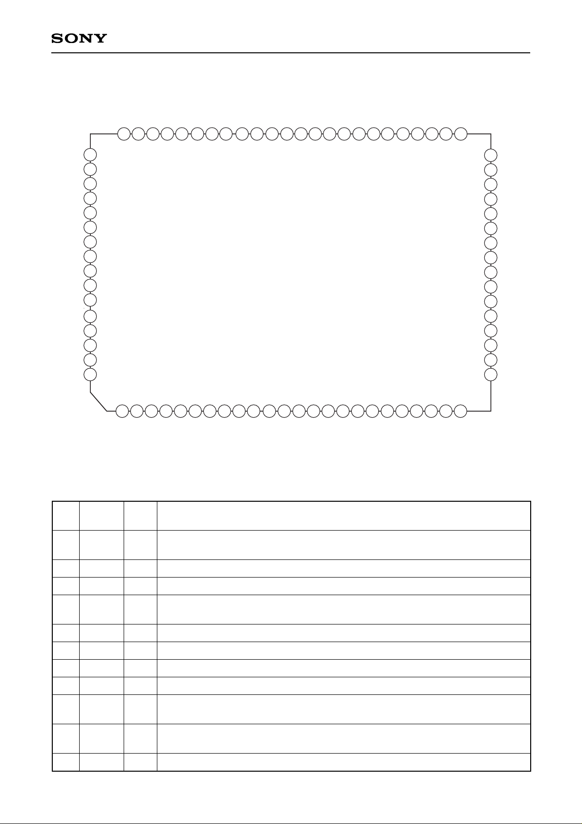
Block Diagram
Recommended Operating Conditions
• Supply voltage DVDD 5.0 ± 0.25 V
YVDD 5.0 ± 0.25 V
CVDD 5.0 ± 0.25 V
PVDD 5.0 ± 0.25 V
• Operating temperature
Topr –20 to +75 °C
Structure
Silicon gate CMOS IC
Applications
Y/C separation for color TVs and VCRs
– 1 –
CXD2043Q
E95812-ST
Digital Comb Filter (NTSC)
Sony reserves the right to change products and specifications without prior notice. This information does not convey any license by
any implication or otherwise under any patents or other right. Application circuits shown, if any, are typical examples illustrating the
operation of the devices. Sony cannot assume responsibility for any problems arising out of the use of these circuits.
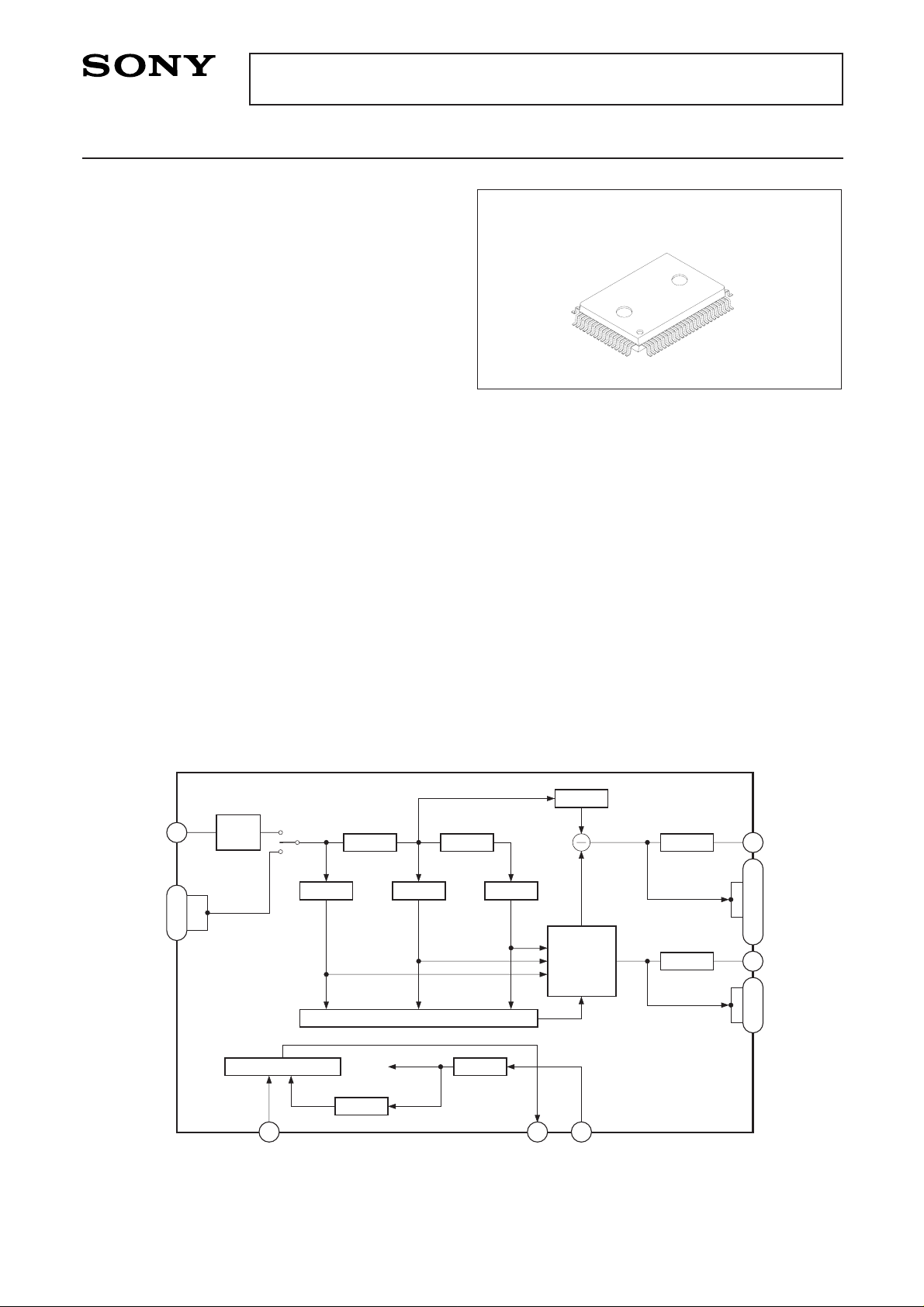
80 pin QFP (Plastic)
27
71
to
78
31
41
VI8 to VI1
ADIN
A/D
BPF BPF BPF
1HDL1HDL
DL
DAC
DAC
Adaptive
Filter
Operation
Logic Operation
VCO
Phase Comparison
1/4
4FSC
C8 to C1
ACO
Y8 to Y1
AYO
43
to
48
·
51
·
52
54
to
61
9
10
12
VCVCPOFIN
For the availability of this product, please contact the sales office.
– 2 –
CXD2043Q
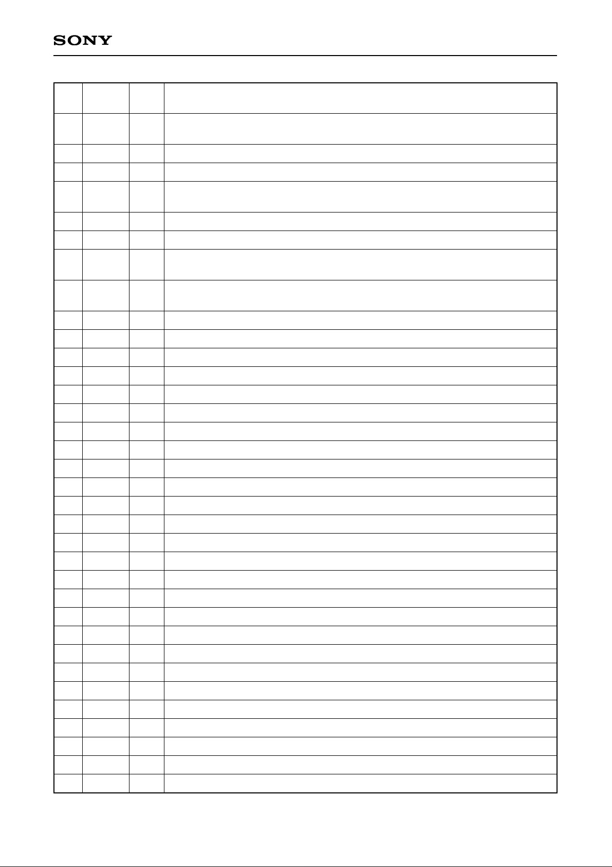
Pin Configuration
Pin Description
Pin
No.
1
2
3
4
5
6
7
8
9
10
11
OCLK
DVSS
DVDD
CLKO
MCK
ADCK
CK4
TEST
FIN
CPO
PVSS
I
—
—
O
I
I
O
I
I
O
—
Clock amplifier input.
Input at 0.8Vp-p or more by eliminating DC components with a capacitor.
Digital ground
Digital power supply
Clock amplifier output.
Left open when the clock amplifier is not used.
Master clock input
Clock input for A/D converter. Input the same clock signal as for Pin 5.
4FSC clock output. Generated from the built-in 4-PLL.
Test. Fix to Low.
FSC clock input. Input FSC which is burst-locked.
Connect to DVss when the PLL is not used.
Phase comparison output for the built-in PLL.
Left open when the PLL is not used.
PLL analog ground
Symbol I/O Description
2
3
4
5
6
7
8
9
10
11
12
13
14 15
16
17
18
19
20
21
22
23
24
25
26
27
28
29
30
40
39
38
37
36
35
34
31
32
33
41
42
43
44
45
46
47
48
49
50
51
52
53
54
55
56
57
58
59
60
70
69
68
67
63
64
65
66
61
62
71
72
73
74
75
76
77
78
79
80
1
OCLK
DV
SS
DV
DD
CLKO
MCK
ADCK
CK4
TEST
FIN
CPO
PV
SS
VCV
TEST
TEST
VCEN
TEST
PV
DD
CLPI
CPON
ADVD
ADVS
ICP
CRV
GR
TST
APCN
XCOE
C1
C2
C3
C4
C5
C6
C7
C8
XYOE
Y1
Y2
DV
DD
DV
SS
Y3
Y4
Y5
Y6
Y7
Y8
CVSS
ACO
CVDD
CVG
CVRF
CIRF
VB
YIRF
YVRF
YVG
YVDD
AYO
YVSS
RT
AAVD
ADIN
AAVS
RB
DV
SS
DVDD
TEST
TEST
TEST
BPF
VI8
VI7
VI6
VI5
VI4
VI3
VI2
VI1
ADCO
INSL
– 3 –
CXD2043Q
Pin
No.
12
13
14
15
16
17
18
19
20
21
22
23
24
25
26
27
28
29
30
31
32
33
34
35
36
37
38
39
40
41
42
43
44
45
VCV
TEST
TEST
VCEN
TEST
PVDD
CLPI
CPON
ADVD
ADVS
ICP
CRV
GR
RB
AAVS
ADIN
AAVD
RT
YVSS
AYO
YVDD
YVG
YVRF
YIRF
VB
CIRF
CVRF
CVG
CVDD
ACO
CVSS
Y8
Y7
Y6
I
I
I
I
O
—
I
I
—
—
I
I
—
O
—
I
—
O
—
O
—
O
I
I
O
O
I
O
—
O
—
O
O
O
Control voltage input for the built-in VCO oscillation.
Connect to PVss when the PLL is not used.
Test. Fix to Low.
Test. Fix to Low.
Built-in VCO oscillation enable. Connect to PVDD when using the PLL.
Connect to PVss when the PLL is not used.
Test. Left open.
PLL analog power supply
Clamp pulse input for A/D converter (negative polarity).
Connect to DVDD when the clamp is off.
High: Clamp function is set to off, and only the normal A/D converter function is enabled.
Low: Clamp function is enabled.
Digital power supply for A/D converter
Digital ground for A/D converter
Clamp control voltage
Clamp reference voltage input
Connect to analog ground.
A/D converter reference voltage (bottom)
Analog ground for A/D converter
Comb filter analog input (A/D converter input)
Analog power supply for A/D converter
A/D converter reference voltage (top)
Analog ground for Y-D/A converter
Analog luminance signal output
Analog power supply for Y-D/A converter
Connect to YVDD via a capacitor of approximately 0.1µF.
VRF for Y. Sets the output full-scale value for Y.
Connect a resistor of 16 times (16R) that of the output resistor "R" of AYO pin.
Connect to YVss via a capacitor of approximately 0.1µF.
Connect a resistor of 16 times (16R) that of the output resistor "R" of ACO pin.
VRF for C. Sets the output full-scale value for C.
Connect to CVDD via a capacitor of approximately 0.1µF.
Analog power supply for C-D/A converter
Analog chroma signal output
Analog ground for C-D/A converter
Digital luminance signal output (MSB)
Digital luminance signal output
Digital luminance signal output
Symbol I/O Description
– 4 –
CXD2043Q
Pin
No.
46
47
48
49
50
51
52
53
54
55
56
57
58
59
60
61
62
63
64
65
66
67
68
69
70
71
72
73
74
75
76
Y5
Y4
Y3
DVSS
DVDD
Y2
Y1
XYOE
C8
C7
C6
C5
C4
C3
C2
C1
XCOE
APCN
TST
DVSS
DVDD
TEST
TEST
TEST
BPF
VI8
VI7
VI6
VI5
VI4
VI3
O
O
O
—
—
O
O
I
O
O
O
O
O
O
O
O
I
I
I
—
—
I
I
I
I
I
I
I
I
I
I
Digital luminance signal output
Digital luminance signal output
Digital luminance signal output
Digital ground
Digital power supply
Digital luminance signal output
Digital luminance signal output (LSB)
Digital luminance signal output control
High: High impedance
Low: Standard output
Digital chroma signal output (MSB)
Digital chroma signal output
Digital chroma signal output
Digital chroma signal output
Digital chroma signal output
Digital chroma signal output
Digital chroma signal output
Digital chroma signal output (LSB)
Digital chroma signal output control.
High: High impedance
Low: Standard output
Aperture compensation switching.
High: Aperture compensation ON
Low: Aperture compensation OFF
Y output through mode.
High: Outputs the input composite video signal from the Y output. At this time,
there is 1H + 18 clock delay from the input.
Low: Y/C separation mode
Digital ground
Digital power supply
Test. Fix to Low.
Test. Fix to Low.
Test. Fix to Low.
High: Fixed to BPF separation
Low: Standard mode
Digital composite video input (MSB)
Digital composite video input
Digital composite video input
Digital composite video input
Digital composite video input
Digital composite video input
Symbol I/O Description
 Loading...