


CXD1961Q
For the availability of this product, please contact the sales office.
DVB-S Front-end IC (QPSK demodulator + FEC)
Description
The CXD1961Q is a single chip DVB Satellite
Broadcasting Front-end IC, including dual ADC for
analog I/O inputs, QPSK demodulator, Viterbi
decoder, de-interleaver, Reed-Solomon decoder
and Energy Dispersal descrambler.
It is suitable for use in a DVB Integrated Receiver
Decoder.
Features
• Dual 6 bit A/D converters
• QPSKdemodulator
Multi-symbol rate operation
Nyquist roll off filter (α = 0.35)
Clock recovery circuit
Carrier recovery circuit
AGC control circuit
• Viterbi decoder
Constraint length K =7
Punctured rate R = 1/2 –7/8
Truncation length 144
Punctured rate search function
BER monitor
• De-interleaver
Packet synchronization
Convolutional de-interleaver
• Reed-Solomon decoder (204, 188)
• Energy dispersal descrambler
• CPU interface
l2C bus interface/8 bit CPU bus
TTL interface level (5V input capability)
• JTAG(IEEE std 1149.1–1990) test mode
• Package : QFP-100pin
• Single +3.3V Power Supply
• Symbol rate max:32MSPS min:TBD
• Power consumption TBD
• 0.4um CMOS Technology
Absolute Maximum Ratings (Ta=25°C, GND=0V)
• Supply voltage VDD –0.5 to 4.6 V
• Input voltage VIN –0.5 to VDD+0.5 V
• Output voltage VOUT –0.5 to VDD+0.5 V
• I/O voltage VI/O –0.5 to VDD+0.5 V
• CPU I/F pin VCPUIF –0.5 to 5.5 V
• Operating temperature Topr 0 to +75 °C
• Storage temperature Tstg –55 to +150 °C
DC Recommended Operating Conditions
(Ta=0°C to 75°C, GND=0 V)
• Supply voltage VDD 3.15 to 3.45 V
• Input Hi-level VIH VDD–0.7 to VDD+0.5V
• Input Lo-level VIL 0.3 to VDD +0.2 V
100 pin QFP (Plastic)
Preliminary
Applications
• DVB-S Set Top Box (Satellite)
Sony reserves the right to change products and specifications without prior notice. This information does not convey any license by
any implication or otherwise under any patents or other right. Application circuits shown, if any, are typical examples illustrating the
operation of the devices. Sony cannot assume responsibility for any problems arising out of the use of these circuits.
—1—
PE96417-TE

Block Diagram
CXD1961Q
81828384858687888990919293949596979899100
1
2
3
Analog I/Q
2ch ADC
Sampling
Clock
VCO
4
5
PLL
6
7
8
Digital
Filter
QPSK
Demodulator
9
10
11
12
Decoder
Viterbi Decoder
CPU I/F
13
14
15
16
17
18
19
20
21
22
23
24
25
26
27
28
29
30
JTAG
Decoded
data & clock
De-interleaver
Reed-Solomon
Energy Dispersal
NCO
l2C
bus
8bit CPU bus
Oscillator
80
79
78
77
76
75
74
73
72
71
70
69
68
67
66
65
64
63
62
61
60
59
58
57
56
55
54
53
52
51
31 32 33 34 35 36 37 38 39 40 41 42 43 44 45 46 47 48 49 50
Typical Application Block Diagram
LNB
VCO
Reference
SAW
PLL
Amp
I/Q
Detector
OSC
Micro Controller
—2—
90°
LPF
LPF
QPSK+FEC
CXD1961Q
LPF
Data
SONY
Clock
Crystal

Pin Configuration
IIN
AVD0
RT0
RB1
AVS1
QIN
AVD1
RT1
92 91 90 89 88 87 86 85 84 83 82 81100 99 98 97 96 95 94 93
AVS2
VCOEN
OPOUT
OPX IN
VCOC
AVD2
11
SS
CPOUT
V
11
DD
V
TEST7
TEST6
10
SS
V
CXD1961Q
AVS0
RB0
V
DD0
V
SS0
CPUSEL
PLLSEL
TEST1
TEST2
TEST3
V
DD1
V
SS1
SDATA
SCLK
SEN
V
DD2
V
SS2
TCK
TMS
TDO
TDI
CK8OUT
RESET
TE
V
DD3
V
SS3
PKTCLK
BYTCLK
PKTERR
DATA0
DATA1
10
11
12
13
14
15
16
17
18
19
20
21
22
23
24
25
26
27
28
29
30
1
2
3
4
5
6
7
8
9
80
79
78
77
76
75
74
72
73
71
70
69
68
67
66
65
64
63
62
61
60
59
58
57
56
55
54
53
52
51
VDD10
CR7
CR6
CR5
CR4
SS9
V
DD9
V
CR3
CR2
CR1
CR0
CKV
AGCPWM
SS8
V
DD8
V
TEST5
TEST4
XI
XO
SS7
V
DD7
V
SDA
SCL
DD3
A
DD2
A
DD1
A
SS6
V
DD6
V
DD0
A
CS
31 32 33 34 35 36 37 38 39 40 41 42 43 44 45 46 47 48 49 50
5
D4
DD
V
5
SS
V
D5
D6
D7
RW
DATA2
DATA3
4
DD
V
DATA4
4
SS
V
DATA5
DATA6
D0
DATA7
D1
D2
D3
—3—
DS
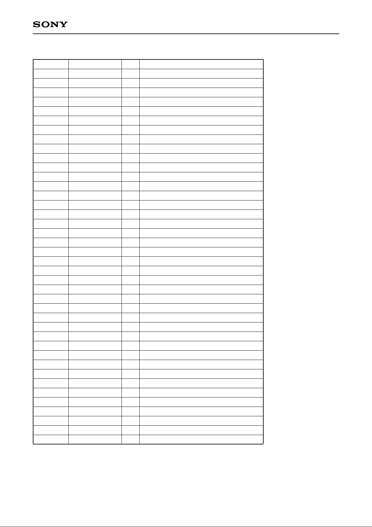
Pin Description
No. Symbol I/O Description
1 AVS0 — Analog Ground
2 RB0 — ADC0 bottom reference voltage
3VDD0 — Digital Power Supply (+3.3 V)
4VSS0 — Digital Ground
5 CPUSEL I CPU interface select (L : I2C bus)
6 PLLSEL I Connect Digital Ground
7–9 TEST1–3 I Test input (connect Digital Ground)
10 VDD1 — Digital Power Supply (+3.3 V)
11 VSS1 — Digital Ground
12 SDATA O SONY internal use
13 SCLK O SONY internal use
14 SEN O SONY internal use
15 VDD2 — Digital Power Supply (+3.3 V)
16 VSS2 — Digital Ground
17 TCK I JTAG test clock
18 TMS I JTAG test mode select
19 TDO O JTAG test data output
20 TDI I JTAG test data input
21 CK8OUT O Divide by 8 clock of Crystal clock
22 RESET I Reset input (L : reset)
23 TE I Test Enable (H : test enable)
24 VDD3 — Digital Power Supply (+3.3 V)
25 VSS3 — Digital Ground
26 PKTCLK O R/S Packet clock
27 BYTCLK O R/S Byte clock
28 PKTERR O R/S uncorrectable Packet flag
29–33 DATA0–4 O R/S data output (DATA0 : LSB)
34 VDD4 — Digital Power Supply (+3.3 V)
35 VSS4 — Digital Ground
36–38 DATA5–7 O R/S data output (DATA7 : MSB)
39–43 D0–D4 I/O 8 bit CPU bus data I/O (D0 : LSB)
44 VDD5 — Digital Power Supply (+3.3 V)
45 VSS5 — Digital Ground
46–48 D5–D7 I/O 8 bit CPU bus data I/O (D7 : MSB)
49 RW I 8 bit CPU bus Read/Write (H : Read)
50 DS I 8 bit CPU bus Data strobe
51 CS I 8 bit CPU bus Chip Select
52 ADD0 I 8 bit CPU bus Address0 (LSB)
53 VDD6 — Digital Power Supply (+3.3 V)
54 VSS6 — Digital Ground
CXD1961Q
—4—
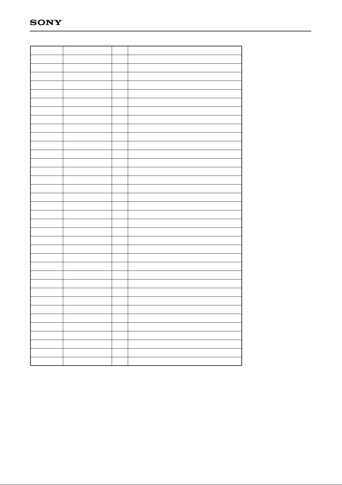
No. Symbol I/O Description
55–57 ADD1–3 I 8 bit CPU bus Address1–3 (ADD3 : MSB)
58 SCL I I2C bus serial clock
59 SDA I/O I2C bus serial data
60 VDD7 — Digital Power Supply (+3.3 V)
61 VSS7 — Digital Ground
62 XO O Oscillator output (for Crystal)
63 XI I Oscillator input (for Crystal)
64, 65 TEST4, 5 O Test output (VSS level)
66 VDD8 — Digital Power Supply (+3.3 V)
67 VSS8 — Digital Ground
68 AGCPWM O PWM output for AGC
69 CKV O Sampling Clock monitor output
70–73 CR0–3 O Clock Recovery data 0–3 (CR0 : LSB)
74 VDD9 — Digital Power Supply (+3.3 V)
75 VSS9 — Digital Ground
76–79 CR4–7 O Clock Recovery data 4–7 (CR7 : MSB)
80 VDD10 — Digital Power Supply (+3.3 V)
81 VSS10 — Digital Ground
82, 83 TEST6, 7 O Test output (VSS level)
84 VDD11 — Digital Power Supply (+3.3 V)
85 VSS11 — Digital Ground
86 CPOUT O PLL Charge pump output
87 AVD2 — Analog Power Supply (+3.3 V)
88 VCOC I VCO control voltage input
89 OPXIN I Embedded OP-Amp Negative input
90 OPOUT O Embedded OP-Amp output
91 AVS2 — Analog Ground
92 VCOEN I VCO enable (H : enable)
93 RT1 — ADC1 top reference voltage
94 AVD1 — Analog Power Supply (+3.3 V)
95 QIN I Analog Q input (ADC1 input)
96 AVS1 — Analog Ground
97 RB1 — ADC1 bottom reference voltage
98 RT0 — ADC0 top reference voltage
99 AVD0 — Analog Power Supply (+3.3 V)
100 IIN I Analog input (ADC0 input)
Note)
Apply 0.1 µF capacitor to every power supply terminal.
Apply 0.1µF capacitor to RB0, RT0, RB1, RT1 for stable A to D conversion.
CXD1961Q
—5—
 Loading...