

Sony CXD1961AQ Datasheet

CXD1961AQ
For the availability of this product, please contact the sales office.
DVB-S Frontend IC (QPSK demodulation + FEC)
Description
The CXD1961AQ is a single chip DVB compliant
Satellite Broadcasting Frontend IC, including dual
A/D converter for analog baseband I/Q input, QPSK
demodulator, Viterbi decoder Reed-Solomon decoder
and Energy Dispersal descrambler. It is suitable for
use in a DVB Integrated Receiver Decoder.
Features
• Dual 6 bit A/D converter
• QPSK demodulator
Multi-symbol rate operation
Nyquist Roll off filter (α = 0.35)
Clock recovery circuit
Carrier recovery circuit
AGC control (PWM output)
• Viterbi decoder
Constraint length 7
Truncation length 144
BER monitor of QPSK demodulator output
• Frame synchronization circuit
• Convolutional de-interleaver
• Reed-Solomon decoder (204,188)
BER monitor of Viterbi decoder output
• Energy dispersal descrambler
• CPU interface circuit
I2C bus interface (5V input capability)
• Package QFP 100pin
• Operating frequency 20 to 30MSPS
• Power consumption 750mW (@3.3V 30MSPS typical)
• Process 0.4µm CMOS Technology
Absolute Maximum Rating (Ta = 25°C, GND = 0V)
• Power Supply VDD –0.5 to +4.6 V
• Input Voltage VIN –0.5 to VDD + 0.5 V
• Output Voltage VOUT –0.5 to VDD + 0.5 V
• I/O Voltage VI/O –0.5 to VDD + 0.5 V
• CPU I/F pin Vcpuif –0.5 to +5.5 V
• Storage Temperature Tstg –55 to +150 °C
Recommended Operating Condition
• Power Supply VDD 3.15 to 3.45 V
• Input High level VIH 0.7 × VDD to VDD + 0.5V
• Input Low level VIL 0.3 to 0.2 × VDD V
100 pin QFP (Plastic)
Preliminary
(Ta = 0 to 75°C, GND = 0V)
Application
DVB-S Set Top Box (Satellite)
Sony reserves the right to change products and specifications without prior notice. This information does not convey any license by
any implication or otherwise under any patents or other right. Application circuits shown, if any, are typical examples illustrating the
operation of the devices. Sony cannot assume responsibility for any problems arising out of the use of these circuits.
– 1 –
PE97854-PS
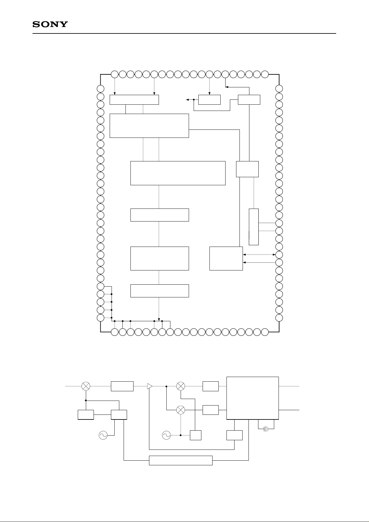
Block Diagram
AVS0
RB0
DD0
V
SS0
V
TEST1
TEST2
TEST3
TEST4
NC
DD1
V
SS1
V
SDAT/SCL
SCLK
SEN/SDA
DD2
V
SS2
V
TCK
TMS
TEST6
TEST7
CK8OUT
RESET
TE
DD3
V
SS3
V
PKTCLK
BYTCLK
PKTERR
DATA0
DATA1
1
2
3
4
5
6
7
8
9
10
11
12
13
14
15
16
17
18
19
20
21
22
23
24
25
26
27
28
29
30
AVD0
IIN
100
99
analog I/O
2ch ADC
decoded data
& clock
RT0
RB1
98
97
Demodulator
RT1
AVD1
QIN
AVS1
93
95
94
96
Sampling
Clock
QPSK
Viterbi Decoder
De-interleaver
Reed-Solomon
Decoder
Energy Dispersal
VCOEN
92
91
AVS2
90
OPXIN
OPOUT
89
VCO
VCOC
88
AVD2
87
CPU I/F
OPOUT
86
85
AVS4
84
AVD4
83
PLL
NCO
QSYNC
FSYNC
82
Oscillator
I2C bus
81
CXD1961AQ
9
SS
V
80
DD9
V
CR7
79
CR6
78
CR5
77
CR4
76
SS8
V
75
DD8
V
74
CR3
73
CR2
72
CR1
71
CR0
70
CKV
69
68
AGCPWM
SS7
V
67
66
DD7
V
65
VCK
VDT
64
XI
63
XO
62
AVS3
61
60
AVD3
SDA
59
SCL
58
TEST22
57
TEST21
56
55
TEST20
SS6
V
54
DD6
V
53
TEST19
52
TEST18
51
Typical Block Diagram
LNB
Reference OSC
31
DATA2
SAW
PLLVCO
32
DATA3
33
DATA4
34
35
37
36
4
4
SS
DD
V
V
DATA6
DATA5
Amp
38
DATA7
40
39
TEST8
I/Q
detector
41
TEST9
TEST10
43
42
TEST11
LPF
44
5
DD
V
TEST12
45
5
SS
V
46
47
TEST14
TEST13
QPSK + FEC
48
TEST15
49
TEST16
50
TEST17
Data
SONY
CXD1961AQ
LPF
Clock
479.5MHz
90°
LPF
Crystal
Micro Controller
– 2 –

CXD1961AQ
Functional Description
(1) A/D Converters
The CXD1961AQ has dual 6 bit A/D converters to quantize the analog baseband I/Q signal. The sampling rate
is two times the symbol rate. The input range is determined by the external resisters. See reference circuit (1).
The DC offset cancellation function is set by setting CPU I/F register 1E,1F(hex).
(2) Clock Recovery Circuit
The CXD1961AQ can operate at multiple symbol rates between 20 to 30MSPS. Initial sampling clock
frequency is set by a 24 bit control word via CPU I/F register 18, 19, 1A (hex). This control word is written to
the numerically controlled oscillator (NCO). The internal clock recovery loop feeds clock error data to the
above NCO to provide sampling timing correction. The relation between the symbol rate and the control word
is;
(symbol rate) = 4 × NCO [23:0] × Fcrystal ÷ 224(Hz)
where NCO [23:0] is the 24 bit control word and Fcrystal is crystal frequency (Hz).
The clock recovery loop coefficient and the loop gain are set by setting CPU I/Fregister 0C (hex) accordingly.
See reference circuit (2). The recovered symbol clock can be monitored at Pin 69.
There are three internal sub-registers to save the NCO control word. By setting the number of the preset subregister, the control word corresponded to the certain symbol rate is set to the internal NCO. Contents of the
sub-register are deleted by power off or reset by pin 22. Refer to the explanation of CPU I/F register 0D (hex).
(3) Carrier Recovery Circuit
Any carrier frequency offset which remains on the analog baseband I/Q input is compensated by the internal
digital costas loop. The capture range is ±Rs/8 (Rs: symbol rate). When the carrier capture is performed,
QPSK lock flag QSYNC goes high. QSYNC is output at Pin 82 and CPU I/F register 09 (hex). In QPSK
synchronization, the carrier offset estimation value is output at CPU I/F register 02 (hex) as AFC [7:0]. The
frequency offset is;
(carrier offset) = Rs × AFC [7:0] ÷ 512 (Hz)
where AFC7 is the sign bit that represents the direction of the offset.
(4) Nyquist Roll off Filter
The Nyquist roll off filter for each channel are embedded. The roll off factor is 0.35.
– 3 –

CXD1961AQ
(5) Auto Gain Control
By comparing the demodulated I/Q amplitude (I2+ Q2) and the reference level which is set via CPU I/F register
21 (hex), the AGC control signal is generated as PWM output at Pin 68. The polarity of the AGC can be
reversed by setting CPU I/F register 10 (hex). For the Tuner interface, see the reference circuit (4).
(6) Viterbi Decoder
The punctured decoding and Viterbi decoding are performed on the demodulated I and Q data. The punctured
rate is programmable from 1/2 to 7/8. When punctured mapping is performed, Viterbi lock flag at CPU I/F
register 09 (hex) goes one. Bit error count at QPSK demodulator output is estimated and output to CPU I/F
register 03, 04 (hex) as 16 bit data.
(7) Frame synchronization and Deinterleaver
By detecting the MPEG2 sync word 47 (hex), the synchronization of the data packet is achieved, and the
convolutional deinterleaver then recovers the original data order.
(8) Reed-Solomon Decoder
In DVB systems, 16 parity bytes are added to the 188 data bytes, so that up to 8 error bytes are correctable by
the Reed-Solomon decoder. If there are more than 8 error bytes in a packet, error correction is not performed
and the packet error flag PKTERR (Pin 28) goes high during the packet to indicate that the packet is not
correctable. The MSB of the second byte of the uncorrectable packet also becomes one. Bit error count at
Viterbi decoder output is estimated and output every 1280 packet (=204 × 8 × 1280 bit) to CPU I/F register 06,
07 (hex) at a resolution of 16 bits.
(9) Energy Dispersal Descrambler
Energy dispersal descrambling is represented by the polynomial X15+ X14+ 1. The initial sequence is loaded
when an inverted MPEG sync word B8 (hex) is detected. When MPEG sync word including inverted one is
detected every 204 bytes, the lock flag of the whole IC "FSYNC" goes high. FSYNC is output at Pin 83 and
CPU I/F register 09 (hex).
– 4 –
CXD1961AQ
(10) CPU Interface
The CXD1961AQ has an I2C bus interface. Serial clock SCL is Pin 58 and serial data in out SDA is Pin 59.
Slave address is "1101 111" (DChex).
<Write data>
During the write operation, the second byte is input as the sub-address of the start position. The third byte then
forms the data to be written to the start register. Successive data bytes are written to the successive subaddress registers up to 21 (hex). Note that registers of sub-addresses 00 (hex) to 0B (hex) are read only.
Slave address
STA
1101 111
0
Sub address
N (hex)
ACK
Input data for
sub-address
ACK
N (hex)
Input data for
sub-address
ACK
N + 1 (hex)
ACK
· · ·
STP
STA: start condition ACK: acknowledge
STP: stop condition XACK: no acknowledge
<Read operation>
Before the read operation, the sub-address of the start register to be read is input by using write operation, and
terminated with a stop condition. Read operation then begins with the second byte which is the data of the start
register. Data of the successive sub-address registers are read successively following the second byte. All
registers can be read.
Slave address
STA
Slave address
STA
1101 111
1101 111
0
1
Sub address
N (hex)
ACK
Output data for
sub-address
ACK
N (hex)
ACK
STP
Output data for
sub-address
ACK
N + 1 (hex)
ACK
· · ·
STP
XACK
Both SCL and SDA have 5V input capability.
– 5 –
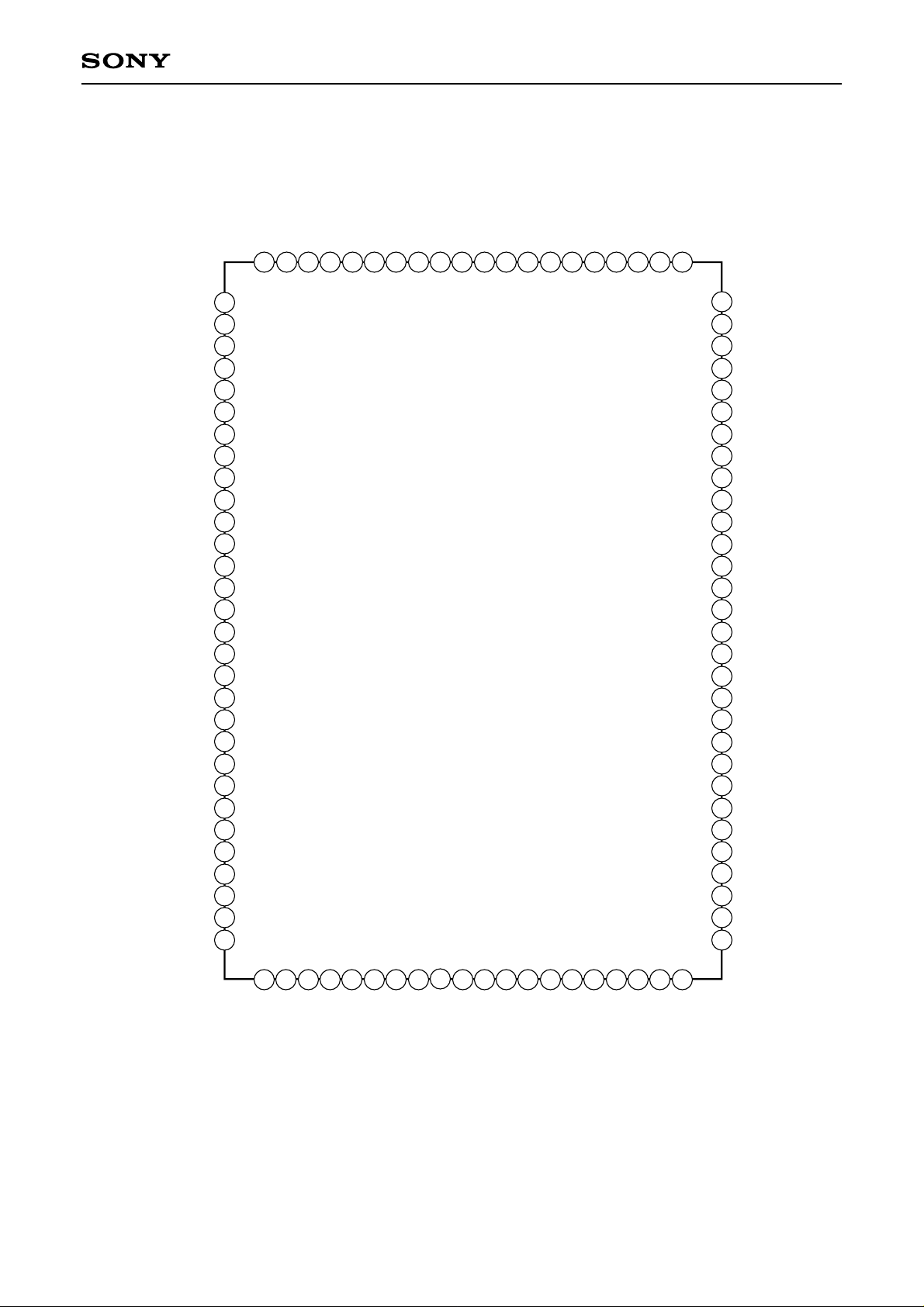
Pin Configuration
AVS0
RB0
DD0
V
SS0
V
TEST1
TEST2
TEST3
TEST4
NC
DD1
V
SS1
V
SDAT/SCL
SCLK
SEN/SDA
DD2
V
SS2
V
TCK
TMS
TEST6
TEST7
CK8OUT
RESET
TE
DD3
V
SS3
V
PKTCLK
BYTCLK
PKTERR
DATA0
DATA1
10
11
12
13
14
15
16
17
18
19
21
22
25
26
27
28
30
20
23
24
29
CXD1961AQ
9
QSYNC
FSYNC
82
81
SS
V
80
79
78
77
76
75
74
73
72
71
70
69
68
67
66
65
64
63
62
61
60
59
58
57
56
55
54
53
52
51
DD9
V
CR7
CR6
CR5
CR4
V
SS8
DD8
V
CR3
CR2
CR1
CR0
CKV
AGCPWM
SS7
V
DD7
V
VCK
VDT
XI
XO
AVS3
AVD3
SDA
SCL
TEST22
TEST21
TEST20
SS6
V
DD6
V
TEST19
TEST18
100
IIN
99
AVD0
98
RT0
97
RB1
96
AVS1
95
QIN
AVD1
94
93
RT1
92
AVS2
VCOEN
90
91
OPXIN
OPOUT
89
VCOC
88
87
AVD2
86
AVS4
OPOUT
84
85
AVD4
83
1
2
3
4
5
6
7
8
9
31
DATA2
32
DATA3
33
DATA4
34
4
DD
V
35
4
SS
V
36
DATA5
37
DATA6
38
DATA7
39
TEST8
– 6 –
40
TEST9
41
TEST10
43
42
TEST11
45
44
5
DD
V
TEST12
5
SS
V
46
48
47
TEST14
TEST13
49
50
TEST16
TEST15
TEST17

Pin List
CXD1961AQ
No.
1
2
3
4
5 to 8
9
10
11
12
13
14
15
16
17
18
19
Symbol I/O type
AVS0
RB0
VDD0
VSS0
TEST1 to 4
NC
VDD1
VSS1
SDAT/SCL
SCLK
SEN/SDA
VDD2
VSS2
TCK
TMS
TEST6
Analog VSS
Ref. voltage input
Digital VDD
Digital VSS
CMOS input
No Connection
Digital VDD
Digital VSS
3-state CMOS output
3-state CMOS output
In out with Pull up
Digital VDD
Digital VSS
Input with pull up
Input with pull up
CMOS input
20
21
22
23
24
25
26
27
28
29 to 33
34
35
36 to 38
39 to 43
44
45
46 to 48
TEST7
CK8OUT
RESET
TE
VDD3
VSS3
PKTCLK
BYTCLK
PKTERR
DATA0 to 4
VDD4
VSS4
DATA5 to 7
TEST8 to 12
VDD5
VSS5
TEST13 to 15
Input with pull up
CMOS output
Input with pull up
Input with pull down
Digital VDD
Digital VSS
3-state CMOS output
3-state CMOS output
3-state CMOS output
3-state CMOS output
Digital VDD
Digital VSS
3-state CMOS output
CMOS in out
Digital VDD
Digital VSS
CMOS in out
49 to 52
TEST16 to 19
CMOS input
– 7 –
CXD1961AQ
No.
53
54
55 to 57
58
59
60
61
62
63
64
65
66
67
68
69
70 to 73
Symbol I/O type
VDD6
VSS6
TEST20 to 22
SCL
SDA
AVD3
AVS3
XO
XI
VDT
VCK
VDD7
VSS7
AGCPWM
CKV
CR0 to 3
Digital VDD
Digital VSS
CMOS input
5V input
5V open drain in out
Crystal VDD
Crystal VSS
Oscillator output
Oscillator input
CMOS in out
CMOS in out
Digital VDD
Digital VSS
CMOS output
CMOS in out
CMOS output
74
75
76 to 79
80
81
82
83
84
85
86
87
88
89
90
91
92
93
VDD8
VSS8
CR4 to 7
VDD9
VSS9
QSYNC
FSYNC
AVD4
AVS4
CPOUT
AVD2
VCOC
OPXIN
OPOUT
AVS2
VCOEN
RT1
Digital VDD
Digital VSS
CMOS output
Digital VDD
Digital VSS
CMOS output
CMOS output
Analog VDD
Analog VSS
3-state CMOS output
Analog VDD
Analog input
Analog input
Analog output
Analog VSS
CMOS input
Ref. voltage input
94
AVD1
Analog VDD
– 8 –

CXD1961AQ
No.
95
96
97
98
99
100
Symbol I/O type
QIN
AVS1
RB1
RT0
AVD0
IIN
Analog input
Analog VSS
Ref. voltage input
Ref. voltage input
Analog VDD
Analog input
Note) Apply 0.1µF capacitor to every power supply terminal and reference voltage input (RB0, RB1, RT0, RT1).
– 9 –
Pin Explanation
1. A/D Converter
CXD1961AQ
Analog signal input
Top reference level input
Bottom reference level input
Analog power supply (+3.3V)
Analog ground
See reference circuit (1)
2. Clock Recovery
2-1. Crystal
Crystal oscillator (output)
Crystal oscillator (input)
Function
ADC for I input
ADC for Q input
Pin No. Pin name Pin No. Pin name
100
98
2
99
1
IIN
RT0
RB0
AVD0
AVS0
95
93
97
94
96
QIN
RT1
RB1
AVD1
AVS1
Pin No.Function Pin name
62
63
XO
XI
Crystal oscillator power supply (+3.3V)
Crystal oscillator ground
See reference circuit (3)
2-2. VCO · OP-Amp
Charge Pump output
Charge pump power supply (+3.3V)
Charge pump ground
VCO control voltage input
VCO enable (H: enable)
OP-Amp negative input
OP-Amp output
VCO · OP-Amp power supply (+3.3V)
VCO · OP-Amp ground
See reference circuit (2)
60
61
AVD3
AVS3
Pin No.Function Pin name
86
84
85
88
92
89
90
87
91
CPOUT
AVD4
AVS4
VCOC
VCOEN
OPXIN
OPOUT
AVD2
AVS2
– 10 –
 Loading...