


IEEE1394 Link Layer LSI for DVB and DSS
For the availability of this product, please contact the sales office.
Description
The CXD1948R is a Link Layer LSI conforming to
the IEEE1394 serial bus standard. During transmission,
the MPEG2 transport stream is time stamped,
transformed to IEEE1394 format and sent to the
IEEE1394 Phy IC.
During reception, the signal from IEEE1394 is kept
in the built-in FIFO, synchronized to the time stamp
value and output.
This IC utilizes Apple Computer’s Fire Wire
technology.
Features
• Conforms to IEEE1394 serial bus standard
• Supports DVB and DSS transport streams
• Dedicated ports for asynchronous data/isochronous
data
• Isochronous data inserted from asynchronous data
port
• Smoothing buffer function
• Large capacity FIFO
Isochronous transmit/receive FIFO 960 × 32 bits
Asynchronous transmit FIFO 30 × 33 bits
Asynchronous receive FIFO 36 × 33 bits
Isochronous Insert Packet Transmit Buffer
47 × 33 bits
• CIP header automatic attachment/detection
Absolute Maximum Ratings (Ta = 25°C)
• Supply voltage VDD Vss – 0.5 to +4.6 V
• Input voltage VI Vss – 0.5 to VDD + 0.5 V
• Output voltage VO Vss – 0.5 to VDD + 0.5 V
• Operating temperature
• Storage temperature
Recommended Operating Conditions
• Supply voltage VDD 3.0 to 3.6 V
• Operating temperature
CXD1948R
100 pin LQFP (Plastic)
Topr –20 to +75 °C
Tstg –55 to +150 °C
Topr –20 to +75 °C
Applications
• Digital interface for D-STB
• Digital interface for D-VHS
Structure
Silicon gate CMOS IC
Fire Wire is a registered trademark of Apple Computer Corporation, USA
Sony reserves the right to change products and specifications without prior notice. This information does not convey any license by
any implication or otherwise under any patents or other right. Application circuits shown, if any, are typical examples illustrating the
operation of the devices. Sony cannot assume responsibility for any problems arising out of the use of these circuits.
– 1 –
E96844-PS

CXD1948R
Contents
1. Block Diagram ............................................................................................................................................... 3
2. Pin Configuration ........................................................................................................................................... 4
3. Pin Description .............................................................................................................................................. 5
4. Electrical Characteristics ............................................................................................................................... 8
4-1. DC Characteristics ................................................................................................................................ 8
4-2. AC Characteristics ................................................................................................................................ 8
4-3. Timing Definitions ................................................................................................................................. 8
5. Isochronous Communication ......................................................................................................................... 9
5-1. Built-in FIFO ......................................................................................................................................... 9
5-2. Transport Stream I/F .......................................................................................................................... 10
5-3. Transport Stream Packet Split and Combine Functions ..................................................................... 18
5-4. Transport Stream ................................................................................................................................ 19
5-5. Isochronous Packet Structure ............................................................................................................ 20
5-6. Relationship between Additional Data and CFR Registers ................................................................ 27
5-7. 27MHz Time Stamp ............................................................................................................................ 27
5-8. Dummy Packet Transmission ............................................................................................................. 28
5-9. Time Stamp ........................................................................................................................................ 29
5-10. Error Processing ............................................................................................................................... 30
5-11. Late Processing ................................................................................................................................ 31
6. Asynchronous Communication .................................................................................................................... 31
6-1. Host/IF ................................................................................................................................................ 31
6-2. CFR .................................................................................................................................................... 34
6-3. Asynchronous Packet Transmission .................................................................................................. 44
6-4. Asynchronous Packet Reception ........................................................................................................ 47
6-5. CXD1948R Data Format .................................................................................................................... 52
6-6. Self-ID Packet Receiving Error Processing ........................................................................................ 62
7. Insert Packet ............................................................................................................................................... 63
7-1. Insert Packet Transmission ................................................................................................................ 63
7-2. Adding a Time Stamp to the Insert Packet ......................................................................................... 66
8. Link-Phy Communication ............................................................................................................................ 67
8-1. Link-Phy Interface Specifications ....................................................................................................... 67
8-2. Communication ................................................................................................................................... 67
9. Parallel Input/Output Port ............................................................................................................................ 74
10. System Configuration Example ................................................................................................................. 75
Annex. Corresponding Table for CFR Access Address And Host Interface I/O Data ..................................... 76
– 2 –
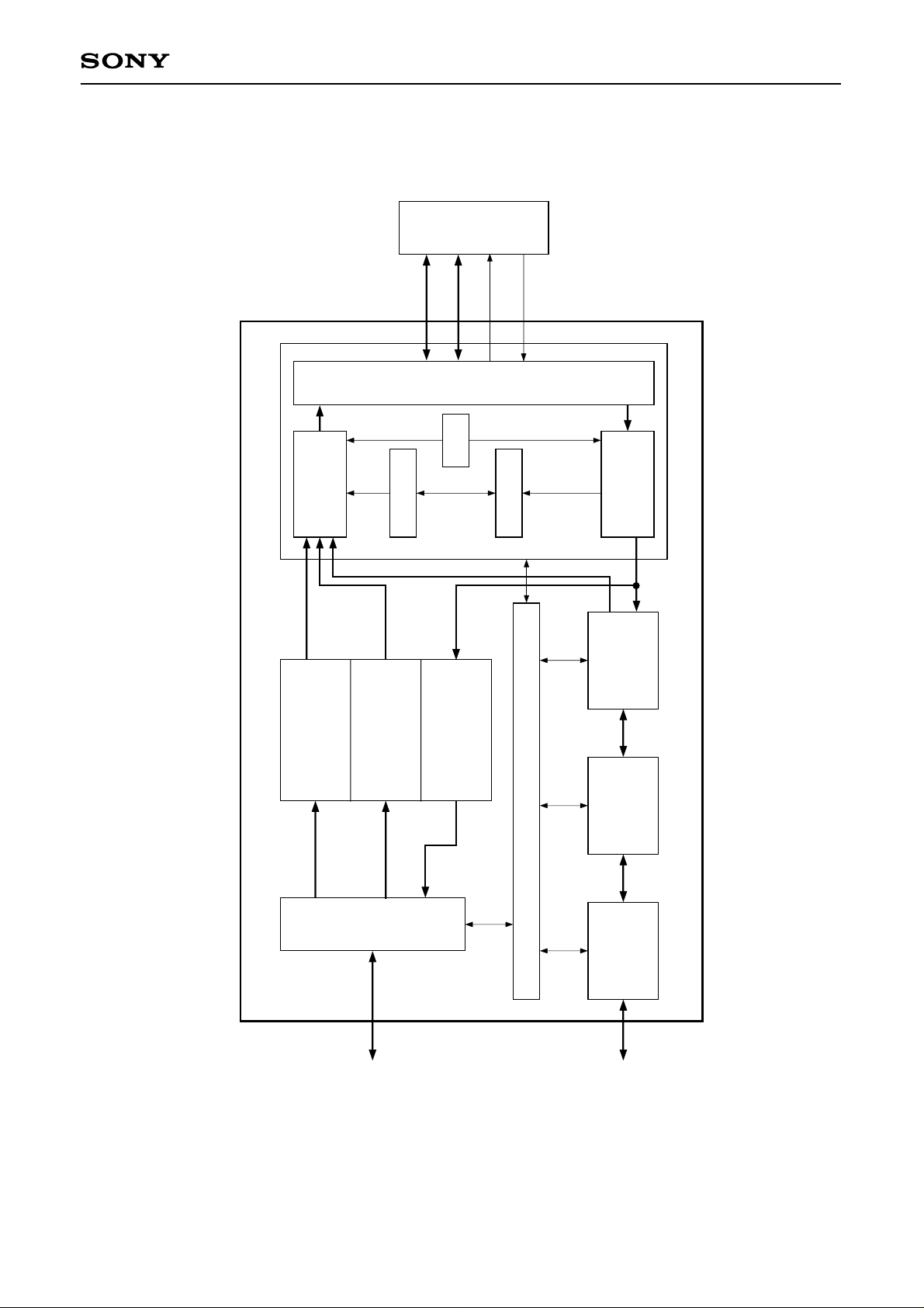
PHY
CXD1948R
Transmitter
FIFO
Transmit
Asynchronous
D [0 : 3]
Cycle Timer
Buffer
Transmit
Insert Packet
LREQ
CTL [0 : 1]
I/F
PHY
CRC
Buffer
Receive
Asynchronous
SYSCLK
Cycle Monitor
Receiver
Detect/
Generate
Header/Sync
Link Core
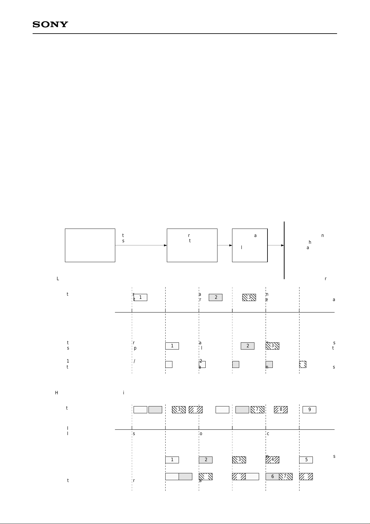
1. Block Diagram
Host
Host
I/F
– 3 –
Receive
Transmit/
Isochronous
Configuration Register
Transport
Data Stream
MPEG2
Transporter
FIFO
I/F
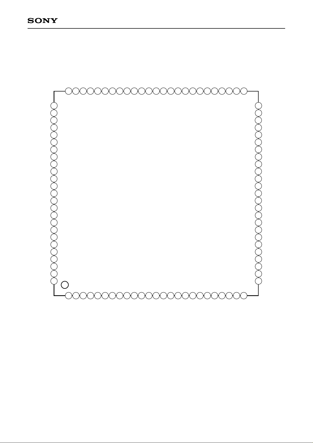
2. Pin Configuration
CXD1948R
VSS
AICK
IFFULL
IFEMPTY
PACKETEN
DD
V
CK27
IOEC
AIDT15
AIDT14
AIDT13
AIDT12
AIDT11
AIDT10
AIDT9
AIDT8
SS
V
AIDT7
AIDT6
AIDT5
AIDT4
AIDT3
AIDT2
AIDT1
AIDT0
76
77
78
79
80
81
82
83
84
85
86
87
88
89
90
91
92
93
94
95
96
97
98
99
100
AIREAD
75
AIWRITE
73
74
READREQ
PACKETGAP
ERRFLAG
72
71
PORT4
70
PORT3
69
TEST19
67
68
LPS
66
DD
V
65
LREQ
64
CTL0
63
CTL1
62
SS
D0
V
D1
60
59
61
D2
58
D3
57
TEST18
TEST17
55
56
TEST15
TEST16
53
54
SS
V
DD
SYSCLK
V
5152
50
TEST14
49
V
48
TEST13
47
TEST12
46
PORT2
45
PORT1
44
PORT0
43
TEST8
42
XINT
41
XW/R
40
XWAIT
39
XCS
38
V
37
ADDRESS0
36
ADDRESS1
35
ADDRESS2
34
ADDRESS3
33
ADDRESS4
32
ADDRESS5
31
ADDRESS6
X8/16
30
XRESET
29
V
28
TEST7
27
TEST6
26
SS
DD
SS
1
SS
V
2
3
DATA15
4
DATA13
DATA14
6
5
DATA12
7
DATA11
DATA10
8
DATA9
9
DATA8
10
DD
V
11
DATA7
12
DATA6
– 4 –
13
DATA5
14 15
DATA4
16
DATA2
DATA3
17
DATA1
18
DATA0
19
SS
V
20
TEST0
21
TEST1
22
TEST2
23
TEST3
24
TEST4
25
TEST5
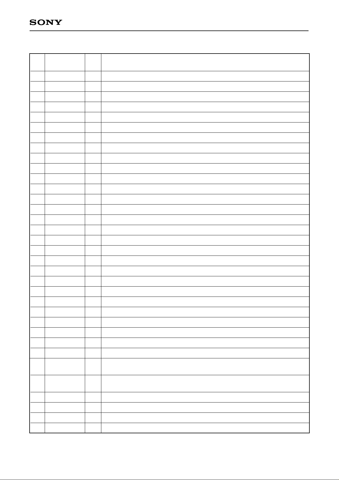
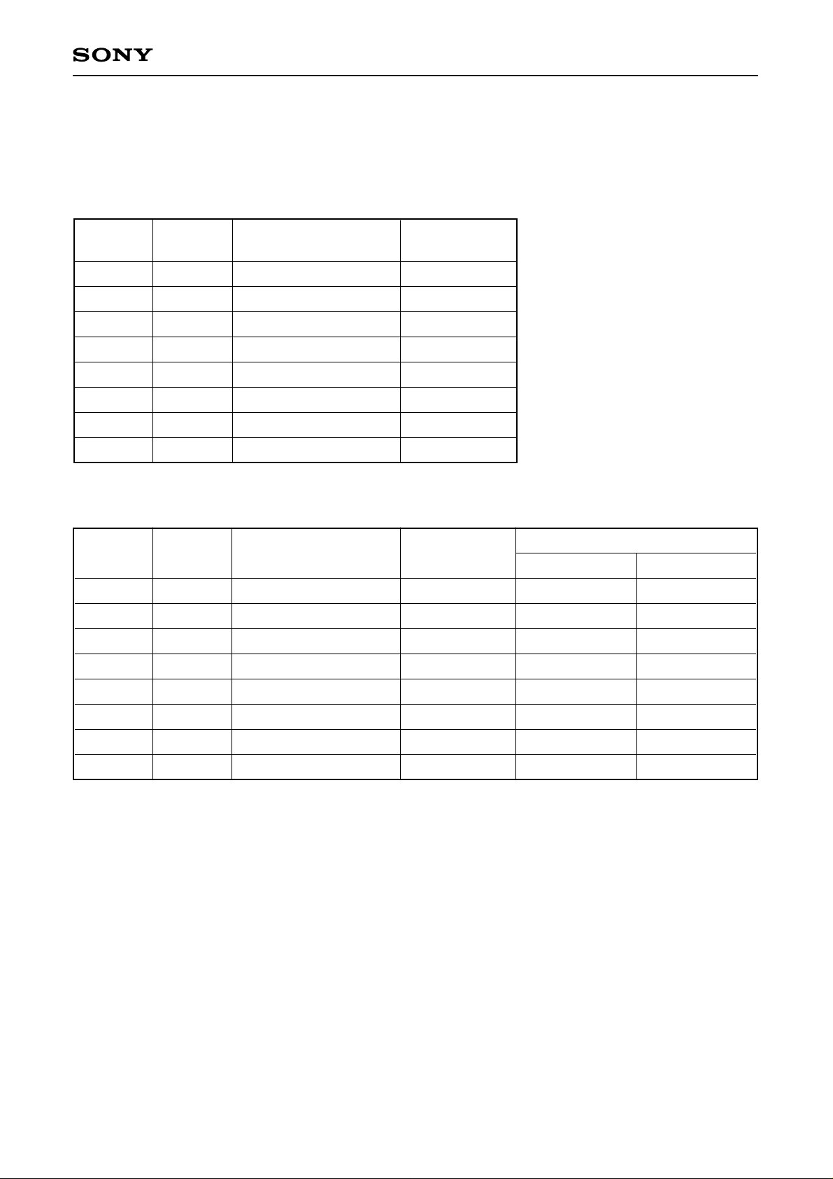
3. Pin Description
CXD1948R
Pin
No.
1
2
3
4
5
6
7
8
9
10
11
12
13
14
15
Symbol I/O
Vss
DATA15
DATA14
DATA13
DATA12
DATA11
DATA10
DATA9
DATA8
VDD
DATA7
DATA6
DATA5
DATA4
DATA3
GND
—
I/O data with host I/F BIT 15
I/O
I/O data with host I/F BIT 14
I/O
I/O data with host I/F BIT 13
I/O
I/O data with host I/F BIT 12
I/O
I/O data with host I/F BIT 11
I/O
I/O data with host I/F BIT 10
I/O
I/O data with host I/F BIT 9
I/O
I/O data with host I/F BIT 8
I/O
Power supply
—
I/O data with host I/F BIT 7
I/O
I/O data with host I/F BIT 6
I/O
I/O data with host I/F BIT 5
I/O
I/O data with host I/F BIT 4
I/O
I/O data with host I/F BIT 3
I/O
Description
16
17
18
19
20
21
22
23
24
25
26
27
28
29
30
DATA2
DATA1
DATA0
Vss
TEST0
TEST1
TEST2
TEST3
TEST4
TEST5
TEST6
TEST7
Vss
XRESET
X8/16
I/O data with host I/F BIT 2
I/O
I/O data with host I/F BIT 1
I/O
I/O data with host I/F BIT 0
I/O
GND
—
Test pin
—
Test pin
—
Test pin
—
Test pin
—
Test pin
—
Test pin
—
Test pin
—
Test pin
—
GND
—
Master reset signal
I
I/O data with host I/F bus select signal
I
∗
∗
∗
∗
∗
∗
∗
∗
0: Active; 1: Non-active
0: 8 bit; 1: 16 bit
ADDRESS6
31
ADDRESS5
32
ADDRESS4
33
ADDRESS3
34
∗
The test pins should be used open.
Host I/F address bus BIT 6
I
Host I/F address bus BIT 5
I
Host I/F address bus BIT 4
I
Host I/F address bus BIT 3
I
– 5 –

CXD1948R
Pin
No.
35
36
37
38
39
40
41
42
43
44
45
46
47
48
Symbol I/O
ADDRESS2
ADDRESS1
ADDRESS0
VDD
XCS
XWAIT
XW/R
XINT
TEST8
PORT0
PORT1
PORT2
TEST12
TEST13
I
Host I/F address bus BIT 2
I
Host I/F address bus BIT 1
I
Host I/F address bus BIT 0
—
Power supply
Host I/F chip select signal
I
O
I
O
—
I/O
I/O
I/O
—
—
0: Active; 1: Non-active
Host I/F wait signal
0: Active; 1: Non-active
Host I/F write/read signal
0: Write; 1: Read
Host I/F interrupt signal
0: Active; 1: Non-active
Test pin
∗
Parallel I/O port BIT0
Parallel I/O port BIT1
Parallel I/O port BIT2
Test pin
Test pin
∗
∗
Description
49
50
51
52
53
54
55
56
57
58
59
60
61
62
63
64
65
VSS
TEST14
VDD
SYSCLK
VSS
TEST15
TEST16
TEST17
TEST18
D3
D2
D1
D0
VSS
CTL1
CTL0
LREQ
—
GND
—
Test pin
—
Power supply
I
Phy I/F system clock (49.152MHz)
—
GND
—
Test pin
—
Test pin
—
Test pin
—
Test pin
I/O
Phy I/F data bus BIT 3
I/O
Phy I/F data bus BIT 2
I/O
Phy I/F data bus BIT 1
I/O
Phy I/F data bus BIT 0
—
GND
I/O
Phy I/F control bus BIT 1
I/O
Phy I/F control bus BIT 0
O
Phy I/F request signal
∗
∗
∗
∗
∗
66
VDD
67
LPS
68
TEST19
∗
The test pins should be used open.
—
Power supply
O
Phy I/F Link power status signal
—
Test pin
∗
– 6 –

CXD1948R
Pin
No.
69
70
71
72
73
74
75
76
77
78
79
80
Symbol I/O
PORT3
PORT4
PACKETGAP
READREQ
ERRFLAG
AIWRITE
AIREAD
VSS
AICK
IFFULL
IFEMPTY
PACKETEN
Description
Parallel I/O port BIT3
I/O
Parallel I/O port BIT4
I/O
Timing signal for adding time stamp to inserted isochronous packet
I
O
I/O
I
I
—
I
O
O
I/O
0: Non-active; 1: Active
Received packet synchronization reference signal
0: Non-active; 1: Active
Packet error signal
0: Non-active; 1: Active
Transport stream I/F data write enable signal
0: Non-active; 1: Active
Transport stream I/F data read enable signal
0: Non-active; 1: Active
GND
Transport stream I/F clock
Isochronous FIFO status output 1: Full
Isochronous FIFO status output 1: Empty
Transport stream I/F packet enable signal
0: Non-active; 1: Active
81
82
83
84
85
86
87
88
89
90
91
92
93
94
95
96
VDD
CK27
IOEC
AIDT15
AIDT14
AIDT13
AIDT12
AIDT11
AIDT10
AIDT9
AIDT8
VSS
AIDT7
AIDT6
AIDT5
AIDT4
Power supply
—
Clock input for 27MHz time stamp (open when not in use)
I
Transport stream I/F data bus control signal
I
I/O
I/O
I/O
I/O
I/O
I/O
I/O
I/O
—
I/O
I/O
I/O
I/O
0: Input; 1: Output
Transport stream I/F data bus BIT 15
Transport stream I/F data bus BIT 14
Transport stream I/F data bus BIT 13
Transport stream I/F data bus BIT 12
Transport stream I/F data bus BIT 11
Transport stream I/F data bus BIT 10
Transport stream I/F data bus BIT 9
Transport stream I/F data bus BIT 8
GND
Transport stream I/F data bus BIT 7
Transport stream I/F data bus BIT 6
Transport stream I/F data bus BIT 5
Transport stream I/F data bus BIT 4
97
AIDT3
98
AIDT2
99
AIDT1
100
AIDT0
∗
The test pins should be used open.
Transport stream I/F data bus BIT 3
I/O
Transport stream I/F data bus BIT 2
I/O
Transport stream I/F data bus BIT 1
I/O
Transport stream I/F data bus BIT 0
I/O
– 7 –
CXD1948R
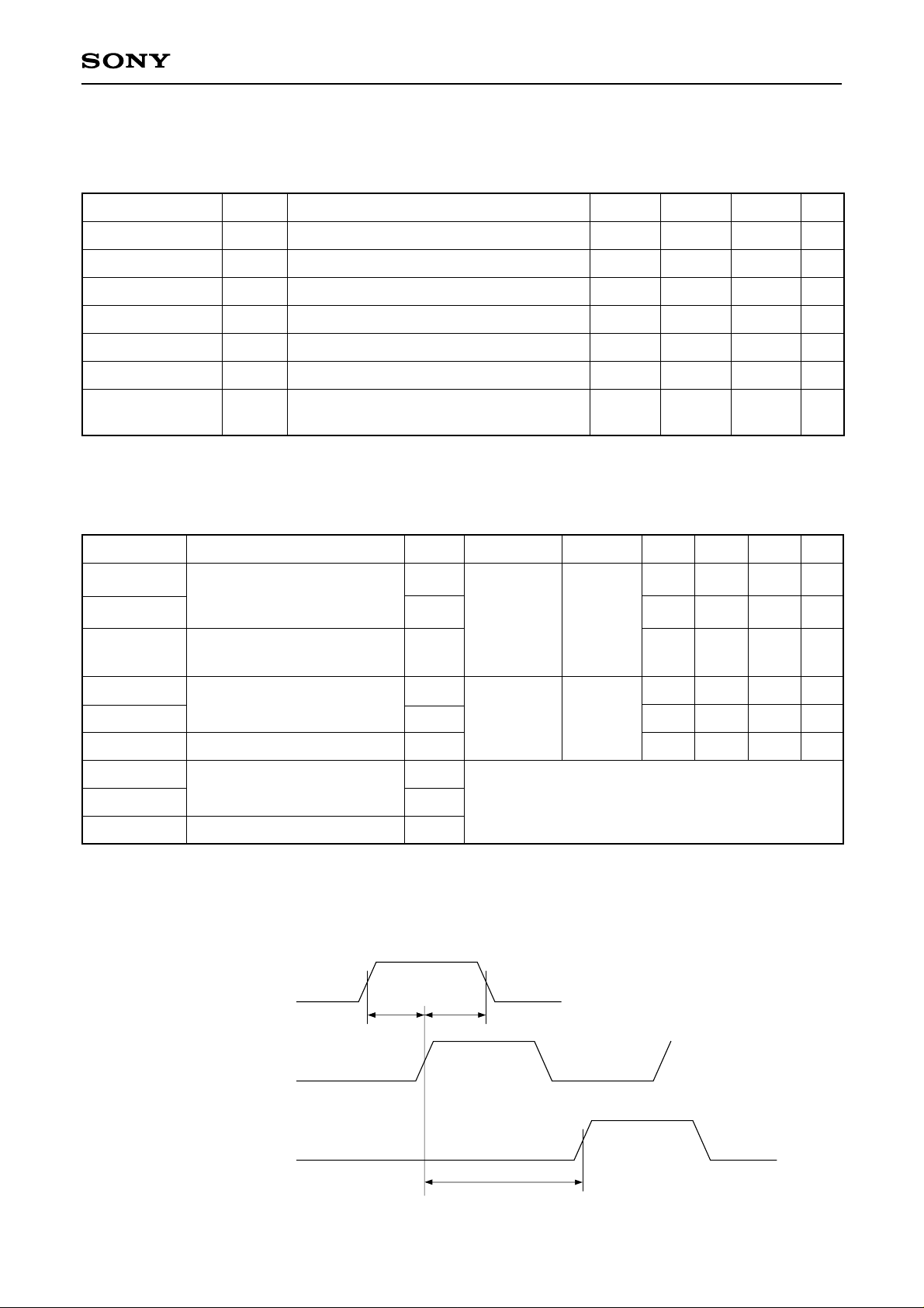
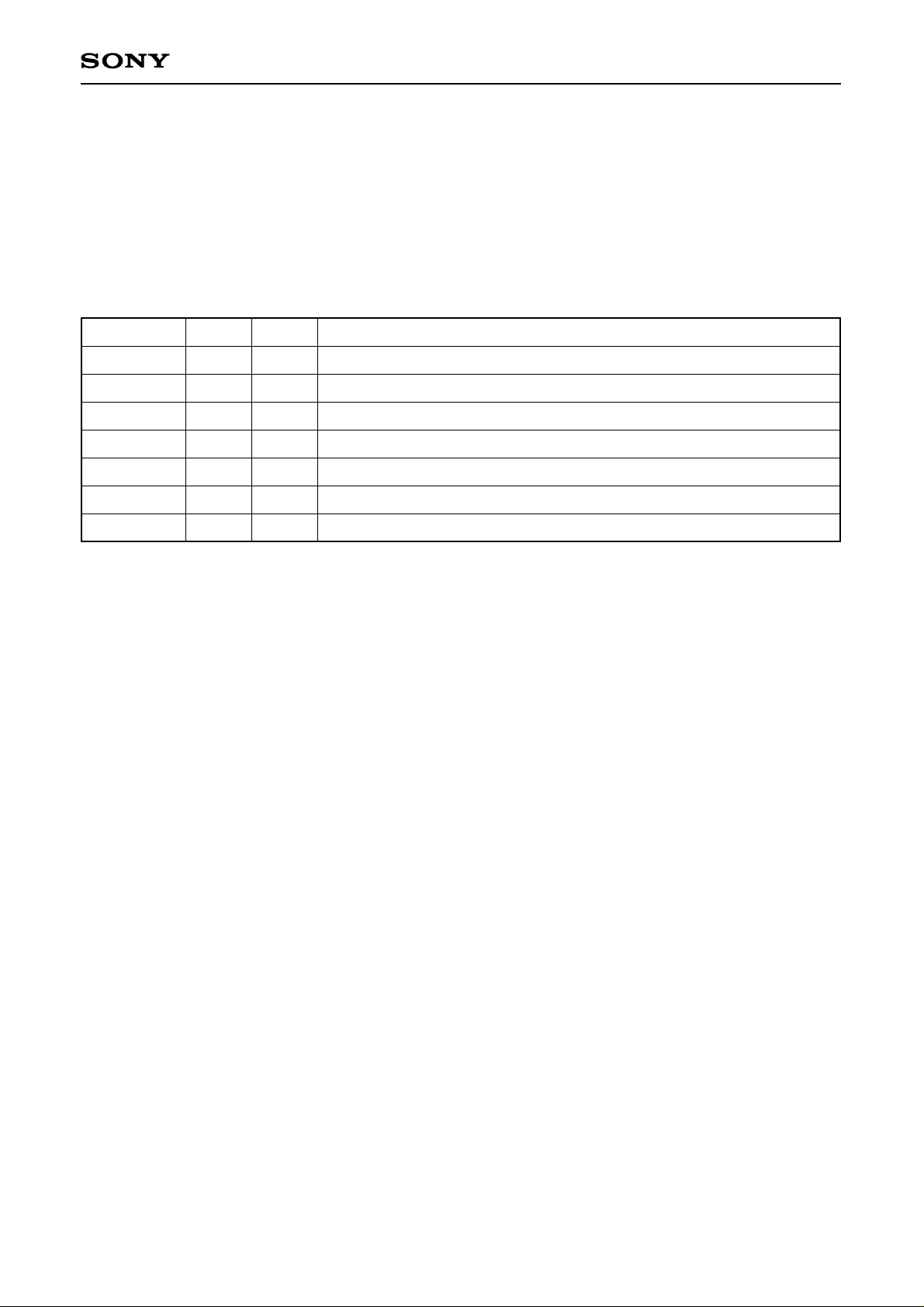
4. Electrical Characteristics
4-1. DC Characteristics (Ta = 25°C, VSS = 0V)
Item Symbol Conditions Min. Typ. Max. Unit
Input voltage
Input voltage
Output voltage
Output voltage
Input leak current
Input leak current
Output leak
current
VIH
VIL
VOH
VOL
II1
II2
IOZ
CMOS input cell
CMOS input cell
IOH = –4.0mA
IOL = 4.0mA
Bidirectional pin (input state)
Normal input pin
Tri-state pin (for high impedance state)
VIN = VSS or VDD
0.7VDD
VDD – 0.4
–40
–10
–40
0.2VDD
0.4
40
10
40
V
V
V
V
µA
µA
µA
4-2. AC Characteristics (VDD = 3.0 to 3.6V)
Item Applicable pin
Input setup
AIDT [15 : 0], ERRFLAG,
PACKETEN, IOEC, AIWRITE,
Input hold
Output delay
AIREAD, PACKETGAP
AIDT [15 : 0], ERRFLAG,
READREQ
Symbol
Tsu1
Th1
Td1
Normal clock
AICK
AIREAD
AIWRITE
∗1
Conditions Min. Typ. Max. Unit
CL = 10pF
10
5
40
ns
0
ns
ns
Input setup
Tsu2
D [3 : 0], CTL [1 : 0]
Input hold
Output delay
Input setup
Input hold
Output delay
∗1
During asynchronous I/F, the reference clock is AIWRITE (transmit)/AIREAD (receive).
D [3 : 0], CTL [1 : 0], LREQ
ADDRESS [6 : 0],
DATA [15 : 0], XCS, XWR
DATA [15 : 0], XWAIT, XINT
Th2
Td2
Tsu3
Th3
Td3
SYSCLK
CL = 10pF
Refer to P.31 ATF/CFR/IPF write timing
ATF/CFR read timing
4-3. Timing Definitions
Input
Tsu Th
reference clock
5
2
2
15
ns
ns
ns
Output
Td
– 8 –
CXD1948R
5. Isochronous Communication
The CXD1948R has a function which transmits and receives DVB and DSS transport stream data as
isochronous packets.
The communication of transport stream data with the DVB and DSS systems is performed using a dedicated
I/O data bus and several control signal pins. (See below.)
Further, it supports a wide variety of application I/F, including 8-bit data and 16-bit data, synchronous and
asynchronous.
Name
AIDT
PACKETEN
ERRFLAG
AIWRITE
AIREAD
READREQ
AICK
Width
16
1
1
1
1
1
1
in/out
in/out
in/out
in/out
in
in
out
in
Description
Transport stream data bus
Indicates a valid packet (valid: 1; invalid: 0)
Indicates that the packet is an error (error: 1; no error: 0)
Data write strobe signal
Data read strobe signal
Packet read request signal
Clock for interface (during sync)
5-1. Built-in FIFO
The CXD1948R has a built-in dedicated FIFO for isochronous communication.
The FIFO capacity is 3840 bytes, and it can accumulate 20 packets worth of DVB transport stream.
In order to actually use the built-in FIFO, the bank structure must be set. This is performed by the CFR
PacketBanks register.
– 9 –
CXD1948R
5-2. Transport Stream Data I/F
5-2-1. Data Bus
The data interface is 8 bit/16 bit, and switching is done by accessing the CFR AIDT16 register. (The default
value is 8 bit.)
5-2-2. Transport Packet Size
Data communication is done in transport stream packet units.
The data size for one packet can be set optionally by accessing the S_PacketSize register on the CFR.
S_PacketSize expresses the byte size of 1 source packet for isochronous communication.
For DVB specifications, this is 192 (data 188 bytes, source packet header 4 bytes).
5-2-3. Isochronous Additional Data
Optional data can be added to the transport stream packet when isochronous communication is performed.
Setting of the additional data is done by setting the CFR AddSize and AddData1 to AddData10 registers.
AddSize is a 4-bit register, and expresses the number of additional bytes for isochronous transmit/receive.
AddData1 to AddData10 are each 8-bit registers, and express the additional data for isochronous transmit/receive.
The default setting is no additional data.
The additional data is inserted between the source packet header and the transport stream data.
The smallest group of data that can be handed under IEEE1394 is 32 bits, so the setting must be such that the
total of the transport stream data and additional data is a 32-bit unit.
An example is shown below.
Example of Isochronous Communication Setting
When S_PacketSize = 192 and AddSize = 0 (example of setting for DVB)
SPH
Transport stream data
188 bytes4 bytes
When S_PacketSize = 144 and TxAddSize = 10 (example of setting for DSS)
SPH
Transport stream data
Additional data 3
Additional data 2
Additional data 1
Additional data 5
Additional data 4
Additional data 6
10 bytes4 bytes
Additional data 9
Additional data 8
Additional data 7
– 10 –
Additional data 10
130 bytes
CXD1948R
5-2-4. Transmit Interface
The CXD1948R is designed for use not only in transmitting an entire input transport stream, but also in
transmitting one program only in the stream. The packet for transmission is selected through PACKETEN input
as in the diagram below.
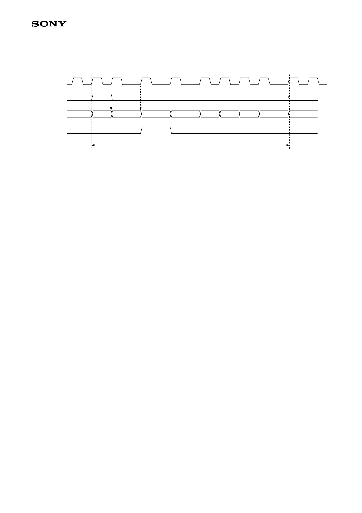
Moreover, constraints are imposed in the packet intervals of streams that can be input to the CXD1948R.
Each time the CXD1948R receives one packet of transport stream data, it adds time stamp data and data from
the host I/F, and there must be an interval of 500ns or more for this processing. The timing is illustrated below.
Also, the PACKETEN input signal must input “HIGH” while the first data of the transport stream packet is being
sent. The maximum period for PACKETENABLE signal high is the period that the transport stream packet data
is valid.
The timing charts for synchronous/asynchronous interface are shown below.
Transmit Interface Limits
AIDT
MPEG2 transporter CXD1948R
Transmission of Program A
AIDT
PACKETEN
A
PACKETEN
B A A
500ns (min)
B A A
– 11 –
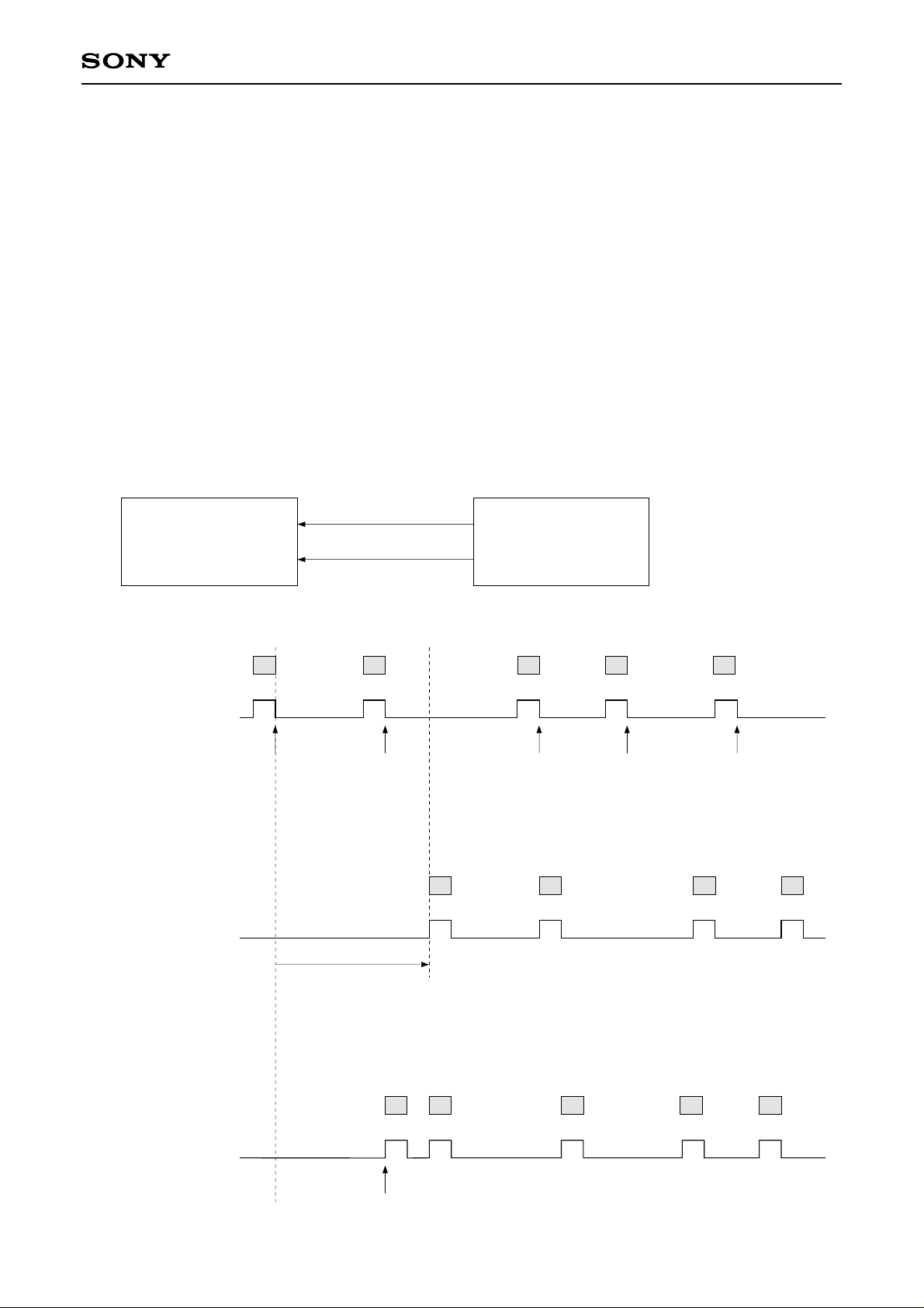
Transmit Interface (for sync mode/8 bit/Nbyte)
AICK
CXD1948R
PACKETEN
AIWRITE
AIDT
ERRFLAG
Don’t Care
first data
taken in
second data
taken in
Valid interval for transport stream packet
Don’t Care
Don’t CareN – 1N – 2N – 3········3210
Sync interface mode is obtained by setting the CFR AsyncAI register to 0. (The default is 0.)
The CXD1948R identifies the first data of the transport stream packet by detecting that the PACKETEN signal
has gone from low to high.
There is no particular need to input the PACKETEN signal after the first data. The size of the data taken in as
valid data is equal to the value set in the CFR S_PacketSize register, decreased by 4 and by the value set in
the AddSize register. The timing for taking in of the data internally is done by AICK rise when AIWRITE is
high.
The AIWRITE signal is used as the enable signal, so the interval that the AIWRITE signal is high relative to
one data must be one AICK clock interval. The interval that the AIWRITE signal is low relative to one data is
not specified.
The limits on AICK input frequency are given below.
For 8-bit data input: 40MHz (Max.), 2MHz (Min.)
For 16-bit data input: 20MHz (Max.), 2MHz (Min.)
The ERRFLAG input during transmit can be made valid by setting the CFR ErrBitEnable register to 1. (The
default is 0.)
The CXD1948R identifies the subject packet as an error if the ERRFLAG input is high for even one data
during transport stream packet valid interval.
The switching timing for ERRFLAG input can be changed in the same way as data switching timing, with
AIWRITE signal rise.
– 12 –
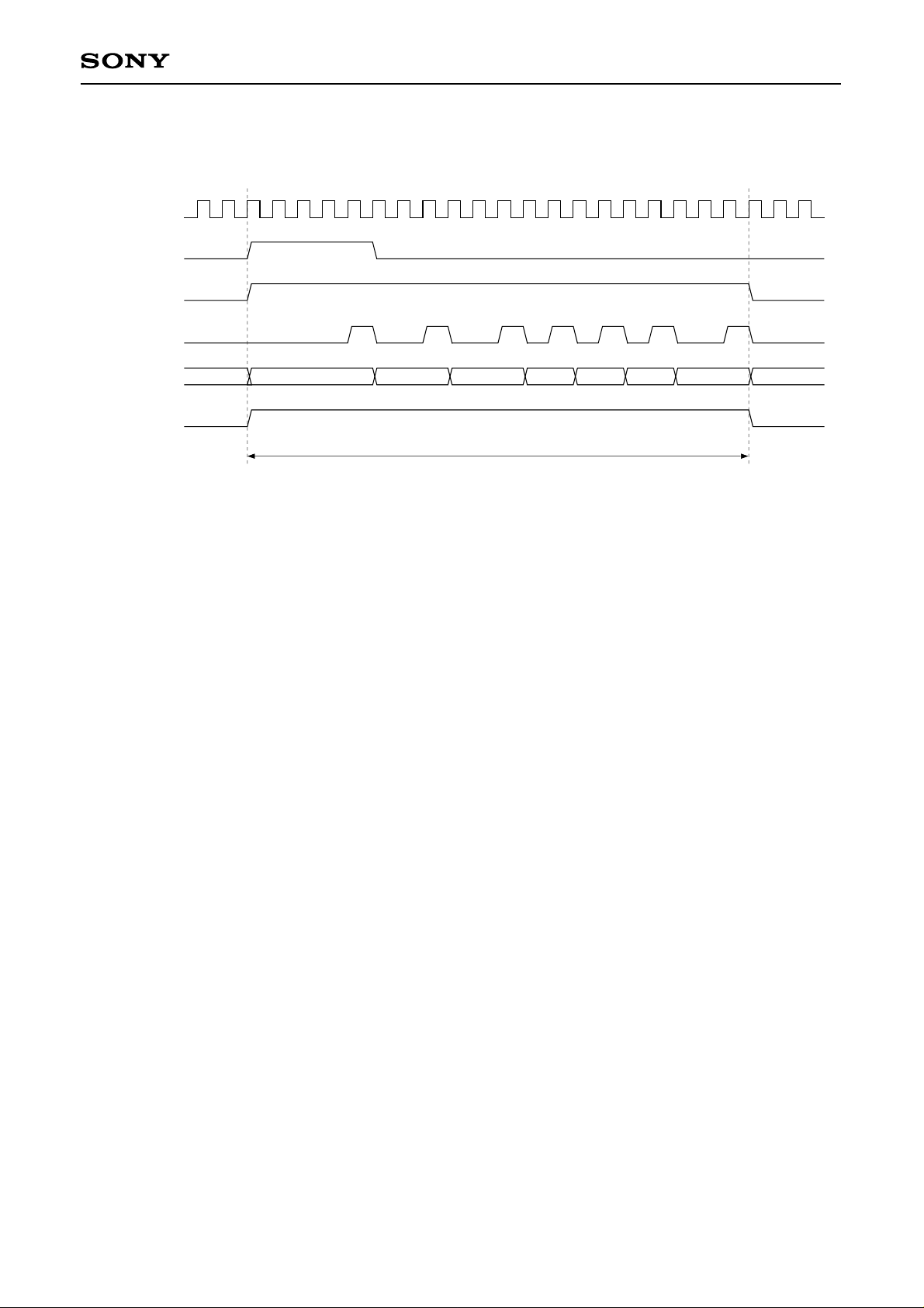
Transmit Interface (for asynchronous mode/8 bit/Nbyte)
AIWRITE
CXD1948R
PACKETEN
AIDT
ERRFLAG
Don’t Care
first data
taken in
second data
taken in
Valid interval for transport stream packet
Don’t Care
Don’t CareN – 1N – 2N – 3········3210
Asynchronous interface mode is obtained by setting the CFR AsyncAI register to 1. (The default is 0.)
The CXD1948R identifies the first data of the transport stream packet by detecting that the PACKET_EN
signal has gone from low to high.
There is no particular need to input the PACKET_EN signal after the first data.
The size of the data taken in as valid data is equal to the value set in the CFR S_PacketSize register,
decreased by 4 and by the value set in the AddSize register. The timing for taking in of the data internally is
done by AIWRITE rise.
The AIWRITE input is used as the clock, so there must be one AIWRITE input rising edge relative to one data.
AIWRITE input duty is not specified, but the AIWRITE input must continue to be input evenly as the clock even
outside of the transport stream packet valid interval.
The limits on AIWRITE input frequency are given below.
For 8-bit data input: 20MHz (Max.), 1MHz (Min.)
For 16-bit data input: 10MHz (Max.), 1MHz (Min.)
The ERRFLAG input during transmit can be made valid by setting the CFR ErrBitEnable register to 1. (The
default is 0.)
The CXD1948R identifies the subject packet as an error if the ERRFLAG input is high for even one data
during transport stream packet valid interval.
The switching timing for ERRFLAG input can be changed in the same way as data switching timing, with
AIWRITE signal rise.
– 13 –
CXD1948R
5-2-5. Receive Interface
The CXD1948R supports two modes; one in which data is output based on the time stamp value added to the
transport stream packet during transmission, and one in which the data is output consecutively as soon as it is
ready, without using the time stamp.
When output is based on the time stamp value, the actual output timing is done using a value which is the time
stamp value with a fixed delay added. This is done in order to keep the packet intervals even on the transmit
and receive sides.
When the time stamp value is not used for output, data output begins when the packet has completely arrived
at the receive side. In this case, the time required for the packet to be sent and arrive completely at the receive
side varies for each isochronous cycle, and packet interval on the transmit side can not be guaranteed.
The timing is shown below.
The mode in which the time stamp is not used can be set by setting the CFR TmsDis register to 1. (The default
is 0.)
Receive Interface
D-VHS system CXD1948R
Transmit I/F
AIDT
PACKETEN
Time stamp
added timing
Receive I/F
Time stamp function used
AIDT
PACKETEN
AIDT
PACKETEN
12
12 34
Fixed delay
3 4
5
Time stamp function not used
AIDT
PACKETEN
12 3 4 5
Time when packet 1
output is ready
– 14 –
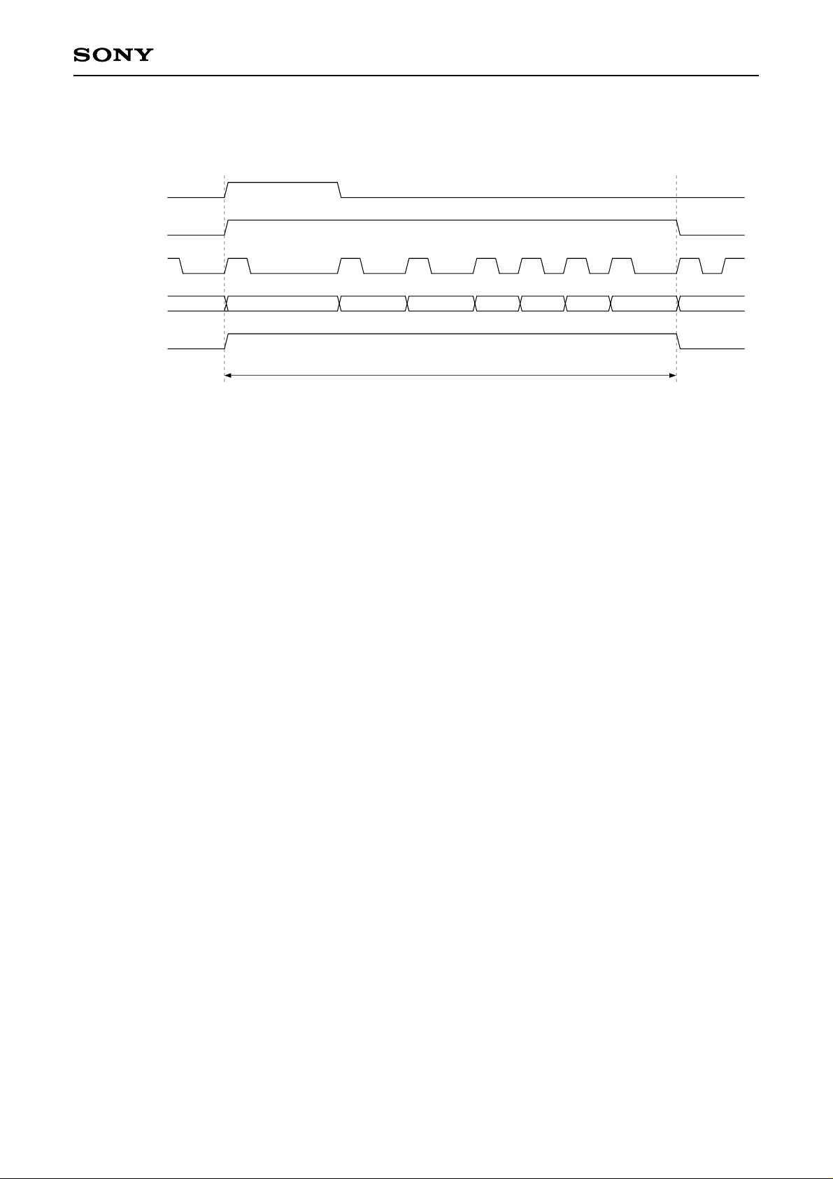
Receive Interface (for sync mode/8 bit/Nbyte)
AICK
READREQ
PACKETEN
AIREAD
CXD1948R
AIDT
ERRFLAG
Don’t Care Don’t CareN – 1N – 2N – 3········210
Valid interval for transport stream packet
Sync interface mode is obtained by setting the CFR AsyncAI register to 0. (The default is 0.)
The CXD1948R outputs the first data of the transport stream packet by changing the READREQ output signal
and PACKETEN output signal from low to high when the packet has been completely received and is ready for
output.
The READREQ output signal goes low when the first data is output.
The same as for transmit, the result of subtracting 4 and the value set in the AddSize register from the value
set in the CFR S_PacketSize register is used as the size of the valid data output in one packet. The timing is
done by the AICK rise when AIREAD is high.
The AIREAD signal is used as the enable signal, so the interval that the AIREAD signal is high relative to one
data must be one AICK clock interval. The interval that the AIREAD signal is low relative to one data is not
specified.
The limits on AICK input frequency are given below.
For 8-bit data input: 40MHz (Max.), 2MHz (Min.)
For 16-bit data input: 20MHz (Max.), 2MHz (Min.)
The ERRFLAG input during receive can be made valid by setting the CFR ErrBitEnable register to 1. (The
default is 0.)
The CXD1948R outputs the ERRFLAG at high during the valid interval if the output transport stream packet is
an error.
The switching timing for ERR_FLAG input can be changed in the same way as data switching timing, with
AIREAD signal rise.
– 15 –
Receive Interface (for asynchronous mode/8 bit/Nbyte)
READREQ
PACKETEN
AIREAD
CXD1948R
AIDT
ERRFLAG
Don’t Care Don’t CareN – 1N – 2N – 3········210
Valid interval for transport stream packet
Sync interface mode is obtained by setting the CFR AsyncAI register to 0. (The default is 0.)
The CXD1948R outputs the first data by changing the READREQ output signal and PACKETEN output signal
from low to high when the packet has been completely received and is ready for output.
The READREQ output signal goes low when the first data is output.
The same as for transmit, the result of subtracting 4 and the value set in the AddSize register from the value
set in the CFR S_PacketSize register is used as the size of the valid data output in one packet. The timing is
done by the AIREAD signal rise.
The AIREAD signal is used as the clock, so there must be one AIREAD input rising edge relative to one data.
AIREAD input duty is not specified, but the AIREAD input must continue to be input evenly as the clock even
outside of the transport stream packet valid interval.
The interval that the AIREAD signal is low relative to one data is not specified.
The limits on AICK input frequency are given below.
For 8-bit data input: 20MHz (Max.), 1MHz (Min.)
For 16-bit data input: 10MHz (Max.), 1MHz (Min.)
The ERRFLAG input during receive can be made valid by setting the CFR ErrBitEnable register to 1. (The
default is 0.)
The CXD1948R outputs the ERRFLAG at high during the valid interval if the output transport stream packet is
an error.
The switching timing for ERR_FLAG input can be changed in the same way as data switching timing, with
AIREAD signal rise.
– 16 –

CXD1948R
5-2-6. Using the ERRFLAG Pin
The CXD1948R can function as a transport stream data interface using error information.
Concretely, this is done using the ERRFLAG pin.
Like other transport stream data interfaces, the ERRFLAG pin is a bidirectional pin. I/O switching is performed
by the CFR IGFMode register.
Also, ERRFLAG control is performed by the CFR ErrBitEn and ErrOutEn registers.
The settings when using ERRFLAG during transmit and receive are given below.
Transmit settings
The ERRFLAG input can be made valid by setting the CFR ErrBitEn register to “1”. (The default is “0”.)
In order to add the error information provided by ERRFLAG to an isochronous packet and transmit this
information, the added data must be 4 bytes or more.
Concretely, the CFR AddSize register value must be 4 or larger.
Both of the conditions below must be met to send error information using the ERRFLAG pin during transmit.
(1) The ErrBitEn register is 1.
(2) The AddSize register is 4 or higher.
Receive settings
The ERRFLAG output can be made valid by setting the CFR ErrOutEn register to “1”. (The default is “0”.)
The CXD1948R handles received packet errors in two ways as follows.
(1) Packets with error information added to the transport stream data
In this case, the error information must be added to the received isochronous packet.
In addition, the CFR ErrBitEn register must be set to 1.
(2) Error packets occurring during isochronous communication
These errors refer to packets received with non-consecutive DBC values due to CRC errors or Late
processing during transmit.
In this case, only the CFR ErrOutEn register is set.
Setting this register to “1” inserts an error packet between packets with non-consecutive DBC values.
As a result, one packet of ERRFLAG = 1 data is read by the transport stream data interface.
If the ErrOutEn register is set to 0, this processing is not performed.
Non-consecutive DBC values also result when the receive FIFO overflows, and the processing is the same
in these cases as well.
– 17 –
CXD1948R
5-3. Transport Stream Packet Split and Combine Functions
The CXD1948R supports split and combine functions in order to use the bus bandwidth effectively.
Concretely, the input transport stream packet can be split or combined according to the input rate and
transmitted as an isochronous packet.
The minimum size which can be split on the CXD1948R is one data block.
For DVB specifications, one data block consists of 24 bytes, which means that 1 packet can be divided into
eighths for transmission.
The maximum size which can be combined is 15 packets. However, if the number of packets which can be
transmitted in that cycle is smaller than the number that can be combined, all the packets present are
combined in the transmission FIFO buffer and transmitted.
The number of data blocks to be transmitted in one isochronous cycle is set before hand according to the
stream peak rate.
This is done by setting values in the CFR NOSP and NODB registers.
The number of transmit source packets in one isochronous cycle is expressed by NOSP, and the number of
transmit data blocks in one isochronous cycle is expressed by NODB.
The default values are NOSP = 0001 and NODB = 000, for transmission of one source packet in one
isochronous cycle. Always be sure to set either NOSP or NODB to 0.
If the isochronous transmission parameters are not set such that the transmission rate is greater than the input
stream peak rate, the FIFO buffer may fail.
Example of Isochronous Transmit using Packet Split and Combine Functions
transport
MPEG2 transporter
Low rate
transport
stream data
IEEE1394
Isochronous
transmit without
splitting
1/2 packet
transmit
stream data
1
CXD1948R
2
1 2
12
12
Physical
layer LSI
3
IEEE1394 bus
3
3
High rate
transport
stream data
IEEE1394
Isochronous
transmit without
combining
2 packet
transmit
12
3
4
12
12
56
3
7
3
4
56
8
4
7
9
5
8
– 18 –
CXD1948R
5-4. Transport Stream Data Bandwidth
The bandwidths on which transport stream data can be transmitted on the CXD1948R are illustrated below.
DVB
DSS
NOSP
value
0000
0000
0000
0001
0010
0011
0100
0101
NOSP
value
0000
0000
NODB
value
001
010
100
000
000
000
000
000
NODB
value
001
010
No. of transmit data
1 data block
2 data blocks
4 data blocks
1 source packet
2 source packets
3 source packets
4 source packets
5 source packets
No. of transmit data
1 data block
2 data blocks
Transmittable
data rate
1.5Mbps
3.0Mbps
6.0Mbps
12.0Mbps
24.0Mbps
36.0Mbps
48.1Mbps
60.1Mbps
Transmittable
data rate
2.2Mbps
4.4Mbps
Transmittable data rate
Addsize = Ah Addsize = 0h
2.0Mbps
4.1Mbps
2.2Mbps
4.4Mbps
0001
0010
0011
0100
0101
0110
000
000
000
000
000
000
1 source packet
2 source packets
3 source packets
4 source packets
5 source packets
6 source packets
8.9Mbps
12.0Mbps
26.8Mbps
35.8Mbps
44.8Mbps
53.7Mbps
8.3Mbps
16.6Mbps
24.9Mbps
33.2Mbps
41.6Mbps
49.9Mbps
8.9Mbps
17.9Mbps
26.8Mbps
35.8Mbps
44.8Mbps
53.7Mbps
– 19 –
CXD1948R
A
A
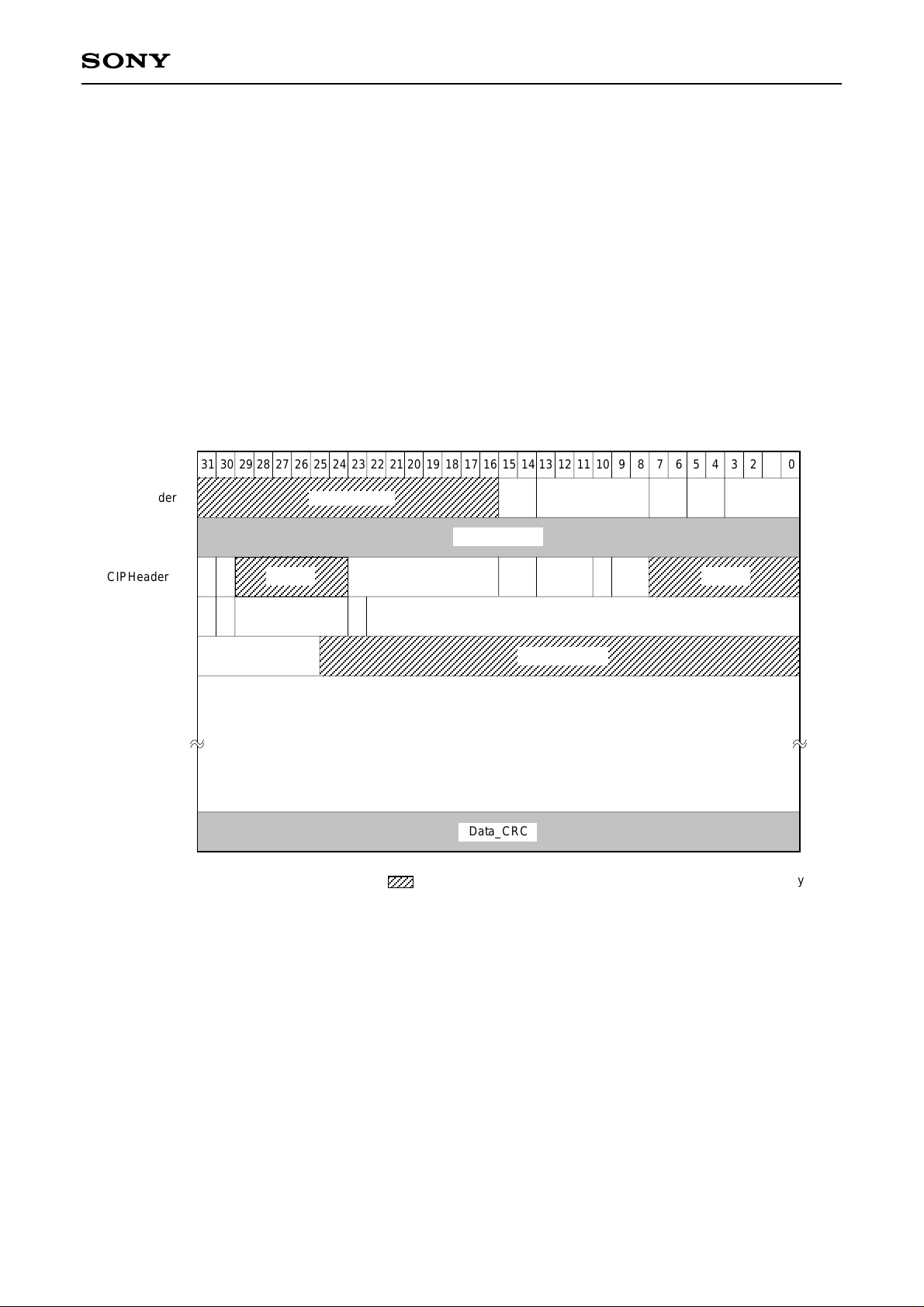
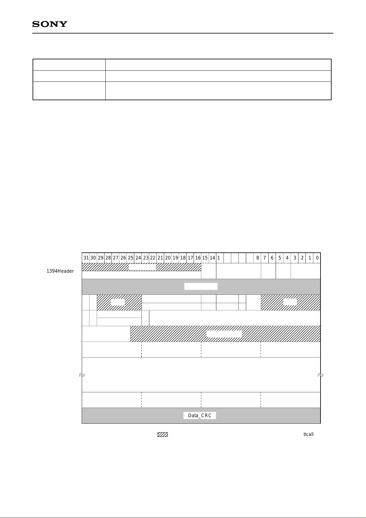
5-5. Isochronous Packet Structure
The basic isochronous packet structure supported by the CXD1948R is illustrated below.
On the CXD1948R, CIPHeaders 1 and 2 are automatically attached/detected in conformity to AV protocol.
Also, a source packet header is automatically added/detected on the transport stream packet based on the
MPEG Data Transmission for IEEE1394 Digital Interface specifications proposed in DVB-SMI.
When one source packet is transmitted in one isochronous cycle, 1st quadlet is 1394Header, 2nd quadlet is
Header_CRC (added at Link Core), 3rd quadlet is CIPHeader1, 4th quadlet is CIPHeader2, 5th quadlet is source
packet header and 6th quadlet and after is the data area. The final quadlet is Data_CRC (added at Link Core).
When a dummy packet is transmitted, there are only 1394Header, Header_CRC, CIPHeader1, CIPHeader2
and Data_CRC.
Basic Structure
031302928272625242322212019181716151413121110987654321
1394Header
CIPHeader1
CIPHeader2
SPHeader
reserved
reserved
speed sytag
DBC
AAA
data length
Header CRC
0 0 QPC
10
Note: The diagonally shaded areas ( ) for 1394Header and CIPHeader1 and 2 are attached automatically by
the CXD1948R. Other areas are set from the external microcomputer via the host I/F.
In transmission from the CXD1948R to an IEEE 1394PHYIC, the four bits marked "reserved" and "speed"
of the 1394Header are automatically replaced by "tcode".
SID
AA
FMT
TF
DBS FN
Data
Data_CRC
channel
SPH
FDF
TimeStampReserved
– 20 –
1394Header Fields
CXD1948R
Field Name
data_length
Indicates the byte length of data from CIPHeader1.
Description
Type of format for data transferred as isochronous packet.
00: no Header
tag
01: format defined by AV protocol
10: Reserved
11: Reserved
channel
Channel number used by the transmitted packet.
Defines transfer speed.
00: 100Mbit/s
speed
01: 200Mbit/s
10: 400Mbit/s
11: Undefined
The CXD1948R supports “00” and “01”.
sy
This field is defined by the application.
Note: The Link Core must be informed of the communication speed in the case of isochronous communication,
so [5 : 4] of [7 : 4], where a tCode is inserted, is used as the speed code. This is replaced with tCode
(1010) at the Link Core.
CIPHeader1 Fields
Field Name
SID
DBS
FN
QPC
SPH
DBC
CIPHeader2 Fields
Field Name
FMT
Description
The CXD1948R Node ID. (0 to 3Fh)
The number of quadlets transferred in one isochronous packet.
For DVB specifications, this is “00000110b” and for DSS specifications, “00001001b”.
Indicates how many data blocks a source packet is divided into.
The number of quadlets added to an incomplete packet when the source packet
is split. Fixed at “0h” on the CXD1948R.
Expresses whether a source packet header is used or not. Fixed at “1” on the
CXD1948R.
Increased by one for each data block. This is a free run continuity counter.
When multiple data blocks are to be sent as a single isochronous packet,
indicates the value for the first data block.
Description
Data format ID.
This is “100000b” for DVB and “100001b” for DSS specifications.
TF
FDF
Indicates whether data is time-shifted. 1 if time-shifted; 0 if not time-shifted.
Used in application defined by FMT.
The value set via the host I/F is input as is on the CXD1948R.
– 21 –
SPHeader fields
CXD1948R
Field Name
Reserved
TimeStamp
The value set via the host I/F is input as is on the CXD1948R.
This is the value of the time that the transport stream packet arrived at the
CXD1948R plus the fixed delay value.
Description
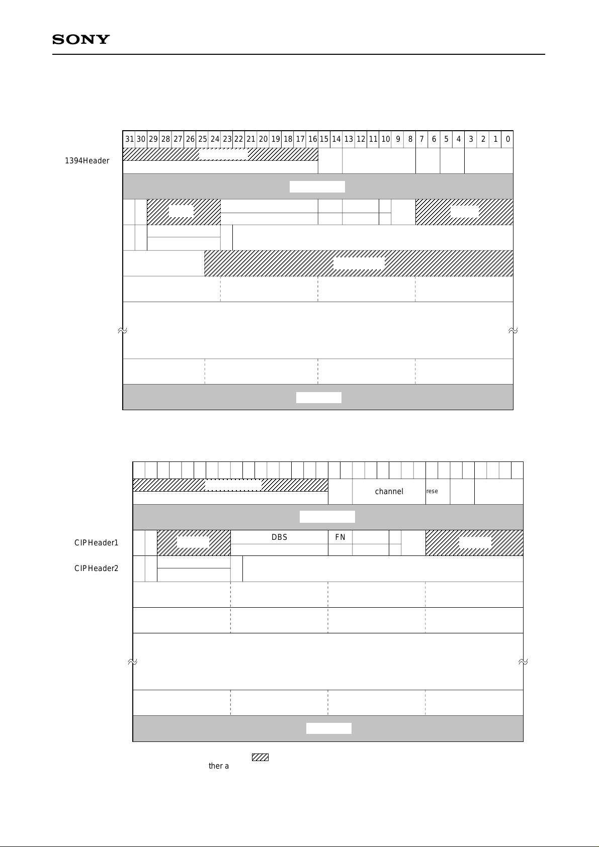
5-5-1. DVB Format
The DVB format supported by the CXD1948R is described below.
The CFR S_PacketSize and AddSize registers are set as shown below when using the CXD1948R in DVB
format.
S_PacketSize: 0C0h
AddSize: 0h
Next, the NOSP and NODB registers are set. These determine how many data are to be transmitted/received
in one isochronous cycle.
The structures of isochronous packets for transmit/receive of data consisting of 1 source packet, 4 data blocks
or 2 source packets in one isochronous cycle are illustrated below.
DVB/Isochronous Packet Structure (1 source packet)
1394Header
CIPHeader1
CIPHeader2
SPHeader
031302928272625242322212019181716151413121110987654321
data_length
00C8h
Header_CRC
00
10
Note: The diagonally shaded areas ( ) for 1394Header and CIPHeader1 and 2 are attached automatically by
the CXD1948R. Other areas are set from the external microcomputer via the host I/F.
In transmission from the CXD1948R to an IEEE 1394PHYIC, the four bits marked "reserved" and "speed"
of the 1394Header are automatically replaced by "tcode".
SID
FMT
20h
Reserved
data0 data1 data2 data3
data184 data185 data186 data187
TF
DBS FN
06h 11 000
Data (188 bytes)
Data_CRC
channel
QPC
FDF
TimeStamp
SPH
1
reserved
reserved
speed sytag
DBC
– 22 –
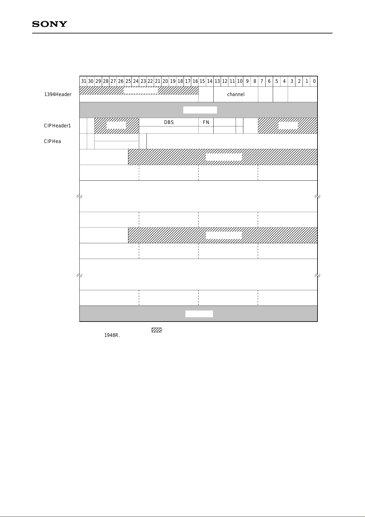
DVB/Isochronous Packet Structure (4 data blocks)
(First half data)
SID
FMT
20h
data_length
0068h
DBS FN
06h 11 000
TF
1394Header
CIPHeader1
CIPHeader2
00
10
Header_CRC
QPC
FDF
channel
SPH
1
reserved
reserved
CXD1948R
031302928272625242322212019181716151413121110987654321
speed sytag
DBC
SPHeader
(Second half data)
1394Header
CIPHeader1
CIPHeader2
TimeStampReserved
data0 data1 data2 data3
Data (92 bytes)
data88 data89 data90 data91
Data_CRC
data_length
0068h
channel
Header_CRC
00
10
SID
FMT
20h
DBS FN
06h 11 000
TF
QPC
FDF
SPH
reserved
1
reserved
031302928272625242322212019181716151413121110987654321
speed sytag
DBC
data92 data93 data94 data95
data96 data97 data98 data99
Data (96 bytes)
data184 data185 data186 data187
Data_CRC
Note: The diagonally shaded areas ( ) for 1394Header and CIPHeader1 and 2 are attached automatically by
the CXD1948R. Other areas are set from the external microcomputer via the host I/F.
In transmission from the CXD1948R to an IEEE 1394PHYIC, the four bits marked "reserved" and "speed"
of the 1394Header are automatically replaced by "tcode".
– 23 –
DVB/Isochronous Packet Structure (2 source packets)
SID
FMT
20h
data_length
0184h
DBS FN
06h 11 000
TF
1394Header
CIPHeader1
CIPHeader2
00
10
Header_CRC
QPC
FDF
channel
SPH
1
reserved
reserved
CXD1948R
031302928272625242322212019181716151413121110987654321
speed sytag
DBC
SPHeader
SPHeader
TimeStampReserved
data0 data1 data2 data3
Data (188 bytes)
data184 data185 data186 data187
TimeSrampReserved
data0 data1 data2 data3
Data (188 bytes)
data184 data185 data186 data187
Data_CRC
Note: The diagonally shaded areas ( ) for 1394Header and CIPHeader1 and 2 are attached automatically by
the CXD1948R. Other areas are set from the external microcomputer via the host I/F.
In transmission from the CXD1948R to an IEEE 1394PHYIC, the four bits marked "reserved" and "speed"
of the 1394Header are automatically replaced by "tcode".
– 24 –
 Loading...