

Sony CXD1914Q Datasheet

—1—
E96Z29-TE
Sony reserves the right to change products and specifications without prior notice. This information does not convey any license by
any implication or otherwise under any patents or other right. Application circuits shown, if any, are typical examples illustrating the
operation of the devices. Sony cannot assume responsibility for any problems arising out of the use of these circuits.
Absolute Maximum Ratings (Ta=25 °C)
• Supply voltage VDD –0.3 to +7.0 V
• Input voltage VI –0.3 to +7.0 V
• Output voltage VO –0.3 to +7.0 V
• Operating temperature Topr –20 to +75 °C
• Storage temperature Tstg –40 to +125 °C
(VSS=0 V)
Recommended Operating Conditions
• Supply voltage VDD 4.75 to 5.25 V
• Input voltage VIN VSS to VDD V
• Operating temperature Topr 0 to +70 °C
I/O Pin Capacitance
• Input pin CI 11 (Max.) pF
• Output pin CO 11 (Max.) pF
Note) Test conditions : VDD=VI=0 V, fM=1 MHz
Description
The CXD1914Q is a digital video encoder
designed for DVDs, set top boxes, digital VCRs and
other digital video equipment. This device accepts
ITU-R601 compatible Y, Cb and Cr data, and the
data are encoded to composite video and separate
Y/C video (S-video) signals and converted to
RGB/YUV signals.
Features
• NTSC and PAL encoding modes
• Composite video and separate Y/C video (S-video)
signal output
• R, G, B/Y, U and V (BetaCam/SMPTE level) signal
output
• 8/16-bit pixel data input modes
• 13.5 Mpps pixel rate
• 10-bit 6-channel DAC
• Supports I2C bus (400 kHz) and Sony SIO
• Closed Caption (Line 21, Line 284) encoding
• Macrovision Pay-Per-View copy protection system
: NTSC Rev. 7.0, PAL Rev. 6.1 (Note 1)
• VBID encoding
• WSS encoding
• Supports non-interlace mode
• Monolithic CMOS single 5.0 V power supply
• 100-pin plastic QFP
Digital Video Encoder
100 pin QFP (Plastic)
CXD1914Q
(Note 1)
This device is protected by U.S. patent numbers 4631603, 4577216 and 4819098 and other intellectual property rights.
Use of the Macrovision anticopy process in the device is licensed by Macrovision for non-commercial home use only.
Reverse engineering or disassembly is prohibited.
For the availability of this product, please contact the sales office.

—2—
CXD1914Q
1/2
Dempx, Level
Translator
and
interpolator
4 : 2 : 2
to
4 : 4 : 4
PDCLK
SYSCLK
PD0-7
PD8-15
XRST
VSYNC
HSYNC
FID
CSYNC
XVRST
SO
SI/SDA
SCK/SCL
XCS/SA
XIICEN
SYNC Gen.
and
Timing Controller
I
2
C-Bus
and
SIO Controller
Internal CLK
LPF
LPF
Delay
Modulator
Sub Carrier
Gen.
BURST FLAG
CSYNC
Closed Caption Encoder
(for NTSC)
MACRO VISION
Signal Gen.
SYNC Slope
Gen.
VBID & WSS
Gen.
YUV/RGB
translator
Inter-
polator
Inter-
polator
10bit
DAC
10bit
DAC
10bit
DAC
10bit
DAC
10bit
DAC
10bit
DAC
JTAG
R/U-OUT
G/Y-OUT
B/V-OUT
COMP-O
Y-OUT
C-OUT
VG
IREF
VREF
VB
TDO
TDI
TMS
TCK
TRST
XTEST1-5
CROMA
Y
U
V
Block Diagram
—3—
CXD1914Q
Pin Description
Pin
Symbol I/O Description
No.
F1
TVSYNC
OSDSW
ROSD
GOSD
BOSD
XVRST
SYSCLK
VSS1
XRST
PDCLK
VDD1
NC
FID
VSYNC
HSYNC
CSYNC
VSS2
PD0
PD1
PD2
PD3
VDD2
I
I
I
I
I
I
I
I
—
I
O
—
—
O
O
O
O
—
I
I
I
I
—
Field ID input.
This signal indicates the field ID when resetting the vertical sync.
“H” indicates 1st field.
“L” indicates 2nd field.
Test pin. Set “L”.
Test pin. Set “L”.
Test pin. Set “L”.
Test pin. Set “L”.
Test pin. Set “L”.
Vertical sync reset input in active low. This pin is pulled up. This is used for
synchronizing the phases of the external and internal vertical sync signals.
When XVRST= “L”, the internal digital sync generator is reset according to the
F1 status.
System clock input.
To generate the correct subcarrier frequency, precise 27 MHz is required.
Digital ground.
System reset input in active low.
Set “L” for 40 clocks (SYSCLK) or more during power-on reset.
Pixel data clock signal output for 13.5 MHz.
A 13.5 MHz signal frequency divided from the system clock (SYSCLK) is output
and used as the clock signal when 16-bit pixel data is input.
Digital power supply.
Not connected inside the IC.
Field ID output.
When control register bit “FIDS” = “1”, “L” indicates 1st field and “H” indicates
2nd field. When control register bit “FIDS” = “0”, “H” indicates 1st field and “L”
indicates 2nd field.
Vertical sync signal output.
Horizontal sync signal output.
Composite SYNC output when using RGB output.
Digital ground.
8-bit pixel data inputs, or lower 8-bit pixel data inputs when 16-bit pixel data is
input. [PD0 to 7]
When control register bit “PIF MODE” = “0”, these are multiplexed Y, Cb, and
Cr signal inputs. When control register bit “PIF MODE” = “1”, these are Y
signal inputs.
Digital power supply.
1
2
3
4
5
6
7
8
9
10
11
12
13
14
15
16
17
18
19
20
21
22
23

—4—
CXD1914Q
Pin
Symbol I/O Description
No.
PD4
PD5
PD6
PD7
NC
NC
NC
NC
NC
PD8 / TD0
PD9 / TD1
PD10 / TD2
PD11 / TD3
VSS3
PD12 / TD4
PD13 / TD5
PD14 / TD6
PD15 / TD7
VDD3
XIICEN
XCS/SA
SCK/SCL
VSS4
I
I
I
I
—
—
—
—
—
I/O
I/O
I/O
I/O
—
I/O
I/O
I/O
I/O
—
I
I
I
—
8-bit pixel data inputs, or lower 8-bit pixel data inputs when 16-bit pixel data is
input. [PD0 to 7]
When control register bit “PIF MODE” = “0”, these are multiplexed Y, Cb, and
Cr signal inputs. When control register bit “PIF MODE" =“1”, these are Y signal
inputs.
Not connected inside the IC.
Not connected inside the IC.
Not connected inside the IC.
Not connected inside the IC.
Not connected inside the IC.
Upper 8-bit pixel data inputs/test data bus when 16-bit pixel data is input.
[PD8 to 15]
When control register bit “PIF MODE” = “0”, these inputs are not used. When
control register bit “PIF MODE” = “1”, these are multiplexed Cb and Cr signal
inputs.
In the test mode, these are used for the internal circuit test data bus. The test
data bus is available only for the device vendor.
Digital ground.
Upper 8-bit pixel data inputs/test data bus when 16-bit pixel data is input.
[PD8 to 15]
When control register bit “PIF MODE” = “0”, these inputs are not used. When
control register bit “PIF MODE” = “1”, these are multiplexed Cb and Cr signal
inputs.
In the test mode, these are used for the internal circuit test data bus. The test
data bus is available only for the device vendor.
Digital power supply.
Serial interface mode select input. This pin is pulled up. When XIICEN = “L”,
Pins 44, 45, 47 and 48 are I2C bus mode.
When XIICEN = “H”, Pins 44, 45, 47 and 48 are Sony SIO mode.
This pin’s function is selected by XIICEN (Pin 43). This pin is pulled up.
When XIICEN = “H”, this pin is Sony SIO mode ; XCS chip select input.
When XIICEN = “L”, this pin is I2C bus mode ; SA slave address select input
which selects the I2C bus slave address.
This pin’s function is selected by XIICEN (Pin 43).
When XIICEN = “H”, this pin is Sony SIO mode ; SCK serial clock input.
When XIICEN = “L”, this pin is I2C bus mode ; SCL input.
Digital ground.
24
25
26
27
28
29
30
31
32
33
34
35
36
37
38
39
40
41
42
43
44
45
46
—5—
CXD1914Q
Pin
Symbol I/O Description
No.
SI/SDA
SO
NC
NC
NC
NC
NC
IREF
VREF
CP-OUT
AVDD1
C-OUT
AVSS1
NC
VB
VG
NC
Y-OUT
AVDD2
B-OUT
AVSS2
NC
NC
NC
NC
G-OUT
AVDD3
R-OUT
AVSS3
NC
NC
NC
NC
NC
VDD4
I/O
O
—
—
—
—
—
I
I
O
—
O
—
—
O
O
—
O
—
O
—
—
—
—
—
O
—
O
—
—
—
—
—
—
—
This pin’s function is selected by XIICEN (Pin 43).
When XIICEN = “H”, this pin is Sony SIO mode ; SI serial data input.
When XIICEN = “L”, this pin is I2C bus mode ; SDA input/output.
This pin’s function is selected by XIICEN (Pin 43).
When XIICEN = “H”, this pin is Sony SIO mode ; SO serial out output.
When XIICEN = “L”, this pin is not used and output is high impedance.
Not connected inside the IC.
Not connected inside the IC.
Not connected inside the IC.
Not connected inside the IC.
Not connected inside the IC.
DAC reference current input.
Connect resistance “16R” which is 16 times output resistance “R”.
DAC reference voltage input.
Sets the DAC output full-scale width.
10-bit DAC output. This pin outputs the composite signal.
Analog power supply.
10-bit DAC output. This pin outputs the chroma (C) signal.
Analog ground.
Not connected inside the IC.
Connect to ground via a capacitor of approximately 0.1 µF.
Connect to analog power supply via a capacitor of approximately 0.1 µF.
Not connected inside the IC.
10-bit DAC output. This pin outputs the luminance (Y) signal.
Analog power supply.
10-bit DAC output. This pin outputs the B and V signals.
Analog ground.
Not connected inside the IC.
Not connected inside the IC.
Not connected inside the IC.
Not connected inside the IC.
10-bit DAC output. This pin outputs the G and Y signals.
Analog power supply.
10-bit DAC output. This pin outputs the R and U signals.
Analog ground.
Not connected inside the IC.
Not connected inside the IC.
Not connected inside the IC.
Not connected inside the IC.
Not connected inside the IC.
Digital power supply.
47
48
49
50
51
52
53
54
55
56
57
58
59
60
61
62
63
64
65
66
67
68
69
70
71
72
73
74
75
76
77
78
79
80
81

—6—
CXD1914Q
Pin
Symbol I/O Description
No.
TD8
TD9
TD10
XTEST1
XTEST2
XTEST3
XTEST4
XTEST5
VSS5
TDI
TMS
TDO
TCK
TRST
VDD5
NC
NC
NC
NC
I/O
I/O
I/O
I
I
I
I
I
—
I
I
O
I
I
—
—
—
—
—
Test data I/Os. These pins should be open.
In the test mode, these are used for the internal circuit test data bus. The test
data bus is available only for the device vendor.
Test mode control signal inputs. These pins are pulled up. When all these
pins are “H”, the CXD1914Q is not in the test mode, but is in the normal mode.
The test mode is available only for the device vendor.
Digital ground.
Test pin. Set “H”. This pin is pulled up.
Test pin. Set “H”. This pin is pulled up.
Test pin. This pin should be open.
Test pin. Set “H”.
Reset signal input for JTAG in active low.
This pin is pulled up.
Digital power supply.
Not connected inside the IC.
Not connected inside the IC.
Not connected inside the IC.
Not connected inside the IC.
82
83
84
85
86
87
88
89
90
91
92
93
94
95
96
97
98
99
100
—7—
CXD1914Q
Electrical Characteristics
DC Characteristics (Ta=0 to +70 °C, VSS=0 V)
Item
Symbol
Measurement
Measurement conditions Min. Typ. Max. Unit
pins
Item Symbol Measurement conditions Min. Typ. Max. Unit
Input High voltage
Input Low voltage
Output High voltage
Output Low voltage
Output High voltage
Output Low voltage
Input leak current
Input leak current
Supply current
VIH
VIL
VOH1
VOL1
VOH2
VOL2
IIL1
IIL2
IDD
∗1
∗1
∗2
∗2
∗3
∗3
∗4
∗5
VDD=5.0 V ±5 %
VDD=5.0 V ±5 %
IOH=–2.4 mA
VDD=4.75 to 5.25 V
IOL=4.8 mA
VDD=4.75 to 5.25 V
IOH=–1.2 mA
VDD=4.75 to 5.25 V
IOL=2.4 mA
VDD=4.75 to 5.25 V
VI=0 to 5.25 V
VDD=4.75 to 5.25 V
VI=0 V
VDD=5.0 V ±5 %
VDD=5.0 V ±5 %
2.2
VDD–0.8
VDD–0.8
–10
–40 –100
0.8
0.4
0.4
10
–240
85
∗6
V
V
V
V
V
V
µA
µA
mA
Note :
∗1 PD0-15, TD8-10, XTEST1-5, TRST, TDI, TMS,TCK, SI/SDA, SCK/SCL, XCS/SA, XVRST, XRST,
SYSCLK, F1, XIICEN, TVSYNC, OSDSW, ROSD, GOSD, BOSD
∗2 PDCLK, VSYNC, HSYNC, FID, SO, CSYNC
∗3 TDO, TD0-10
∗4 PD0-15, TD8-10, TCK, SI/SDA, SCK/SCL, XRST, F1, SYSCLK, TVSYNC, OSDSW,ROSD, GOSD,
BOSD
∗5 XTEST1-5, TRST, TDI, TMS, XCS/SA, XVRST, XIICEN
∗6 Not including analog supply current
DAC Characteristics 1 (AVDD=5 V, R=200 Ω, VREF=2.00V , Ta=25 °C)
Resolution
Linearity error
Differential linearity error
Output full-scale current
Output offset voltage
Output full-scale voltage
Precision guaranteed output
voltage range
n
EL
ED
IFS
VOS
VFS
VOC
–2.0
–1.0
9.5
1.9
1.9
10
10.0
2.0
2.0
2.0
1.0
10.5
1
2.1
2.1
bit
LSB
LSB
mA
mV
V
V

—8—
CXD1914Q
AC Characteristics
1. Pixel data interface
(1) 8-bit mode
tPDS tPDH
SYSCLK
PD0-7
tPDS tPDH
PDCLK
PD0-15
(Ta=0 to +70 °C, VDD=4.75 to 5.25 V, VSS=0 V)
Item Symbol Min. Typ. Max. Unit
Pixel data setup time to SYSCLK
Pixel data hold time to SYSCLK
tPDS
tPDH
10
3
ns
ns
(Ta=0 to +70 °C, VDD=4.75 to 5.25 V, VSS=0 V)
Item Symbol Min. Typ. Max. Unit
Pixel data setup time to PDCLK
Pixel data hold time to PDCLK
tPDS
tPDH
20
0
ns
ns
(2) 16-bit mode
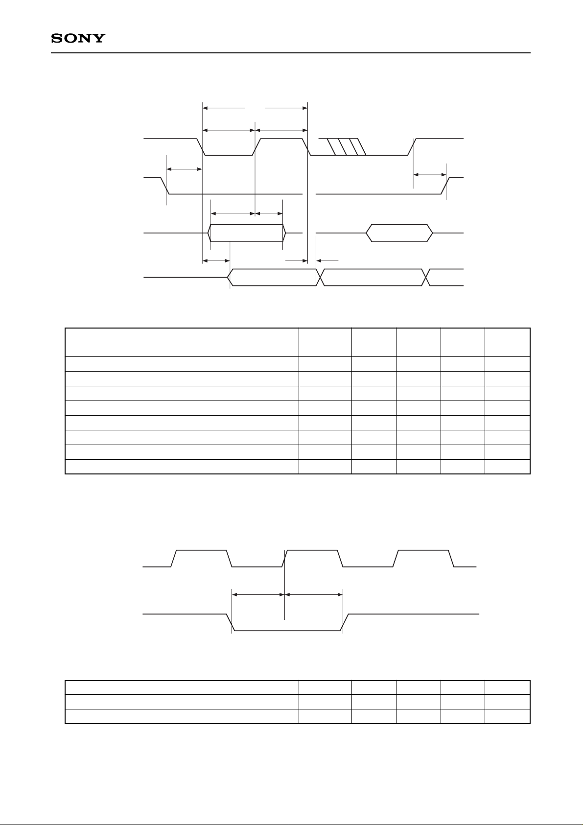
—9—
CXD1914Q
2. Serial port interface
(Ta=0 to +70 °C, VDD=4.75 to 5.25 V, VSS=0 V)
fSCK
tPWLSCK
tPWHSCK
tCSS
tCSH
tSIS
tSIH
tSOD tSOH
SCK
XCS
SI
SO
Item Symbol Min. Typ. Max. Unit
SCK clock rate
SCK pulse width Low
SCK pulse width High
Chip select setup time to SCK
Chip select hold time to SCK
Serial input setup time to SCK
Serial input hold time to SCK
Serial output delay time from SCK
Serial output hold time from SCK
fSCK
tPWLSCK
tPWHSCK
tCSS
tCSH
tSIS
tSIH
tSOD
∗
tSOH
∗
DC
100
100
150
150
50
10
3
3
30
MHz
ns
ns
ns
ns
ns
ns
ns
ns
Item Symbol Min. Typ. Max. Unit
XVRST, F1 setup time to SYSCLK
XVRST, F1 hold time to SYSCLK
tVS
tVH
10
0
ns
ns
∗
CL=35 pF
3. XVRST, F1
tVS tVH
SYSCLK
XVRST
F1

—10—
CXD1914Q
4. SYSCLK, PDCLK, VSYNC, HSYNC, FID, CSYNC
(Ta=0 to +70 °C, VDD=4.75 to 5.25 V, VSS=0 V)
SYSCLK
tPWHCLK tPWLCLK
fSYSCLK
tPDCLKD tPDCLKD
tCOH
tCOD
PDCLK
VSYNC,
HSYNC,
FID,
CSYNC
Item Symbol Min. Typ. Max. Unit
SYSCLK clock rate
SYSCLK pulse width Low
SYSCLK pulse width High
PDCLK delay time from SYSCLK
Control output delay time from SYSCLK
Control output hold time from SYSCLK
fSYSCLK
tPWLCLK
tPWHCLK
tPDCLKD
∗
tCOD
∗
tCOH
∗
11
11
3
27
20
25
MHz
ns
ns
ns
ns
ns
∗
CL=35 pF
—11—
CXD1914Q
Also, the pixel input data timing is determined according to bits 3 and 2 (PIX TIM) of control register
address 01H as shown in Table 1-2 below.
When “PIF MODE” is “0", Cb0 of the image data (Cb0, Y0, Cr0 and Y1) input from PD0 to 7 is sampled at
the rising edge of SYSCLK after the fall of HSYNC.
(Default : Cb0 is sampled at the rising edge of the second SYSCLK after the fall of HSYNC.)
When “PIF MODE” is “1”, Y0 and Y1 data are input to PD0 to 7, multiplexed Cb0 and Cr0 data are input to
PD8 to 15, and Y0 and Cb0 are sampled at the respective rising edge of PDCLK after the fall of HSYNC.
(Default : Y0 and Cb0 are sampled at the rising edge of the second PDCLK after the fall of HSYNC.)
Table 1-2
Description of Functions
The CXD1914Q converts digital parallel data (ITU-R601 Y, Cb, Cr) into analog TV signals in NTSC
(RS170A) or PAL (ITU-R624; B, G, H, I) format.
The CXD1914Q first receives image data in 8-bit parallel form (multiplexed Y, Cb, and Cr data), or in 16-bit
parallel form (8-bit Y and 8-bit multiplexed Cb and Cr data). After demultiplexing, it converts the Cb and Cr
signals into the U and V signals, respectively, interpolates 4 : 2 : 2 to 4 : 4 : 4, and then modulates the
signals with the digital subcarrier inside the CXD1914Q to create the chroma (C) signal.
The Y and chroma (C) signals are oversampled at double speed to reduce sin (X) / X roll-off, and then
added to become the digital composite signal.
The 10-bit DAC converts the digital composite, Y/C, U, V, and RGB signals into analog signals.
1. Pixel input format
The pixel input format is selected according to the value (bit 4 of address 01H) of control register “PIF
MODE” as shown in Table 1-1 below.
When “PIF MODE” is “0”, the image data (multiplexed Y, Cb, and Cr data) input from PD0 to 7 are sampled
at the rising edge of SYSCLK as shown in the chart on the following page. When “PIF MODE” is “1”, the
image data (PD0 to 7 : Y data, PD8 to 15 : multiplexed Cb and Cr data) input from PD0 to 15 are sampled
at the rising edge of PDCLK.
Table 1-1
PIF MODE PD15 to 8 PD7 to 0
0 (8-bit mode) N/A Y/Cb/Cr
1 (16-bit mode) Cb/Cr Y
PIX TIM
0 0
0 1
1 0
1 1
Timing phase
#0 (default)
#1
#2
#3

—12—
CXD1914Q
Pixel Data Input Timing
SYSCLK
PDCLK
Y1 Y2 Y3 Y4 Y5Y0PD0 to 7
HSYNC
Cr0 Cb2 Cr2 Cb4 Cr4Cb0PD8 to 15
# 0 #1
[16-bit mode]
Y1 Y2 Y3 Y4Y0
Cr0 Cb2 Cr2 Cb4Cb0
# 2 #3
PD0 to 7
[8-bit mode]
# 0
Cb0 Y0 Cr0 Y1 Cb2 Y2 Cr2 Y3 Cb4 Y4 Cr4 Y5 Cb6
# 1
Cb0 Y0 Cr0 Y1 Cb2 Y2 Cr2 Y3 Cb4 Y4
# 2
Cb0 Y0 Cr0 Y1 Cb2 Y2 Cr2 Y3 Cb4 Y4 Cr4
# 3
Cb0 Y0 Cr0 Y1 Cb2 Y2 Cr2 Y3 Cb4 Y4 Cr4 Y5
1 2 3 4 5
1 2 3
PD8
PD9
:
PD15
Pixel data 0 (LSB)
Pixel data 1
:
Pixel data 7 (MSB)
PD0
PD1
:
PD7
Pixel data 0 (LSB)
Pixel data 1
:
Pixel data 7 (MSB)

—13—
CXD1914Q
2. Serial interface
The CXD1914Q supports both the I2C bus (high-speed mode) and Sony serial interface modes. These
modes can be selected by the XIICEN input pin as shown in Table 2-1 below.
Table 2-1
XIICEN
SI/SDA
SCK/SCL
XCS/SA
SO
H
SONY SIO Mode
SI
SCK
XCS
SO
L
I2C Mode
SDA
SCL
SA
High-Z
2-1 I2C bus interface
The CXD1914Q becomes an I2C bus slave transceiver, and supports the 7-bit slave address and the
high-speed mode (400 Kbits/s).
2-1-1. Slave address
Two kinds of slave address (88H, 8CH) can be selected by the SA signal as shown in Table 2-2 below.
Table 2-2
A6 A5 A4 A3 A2 A1 A0 R/W
1 0 0 0 1 SA 0 X
2-1-2. Write cycle
After the slave address is supplied from the master, the data in the next transfer cycle is set up inside the
start address register of this IC as the start address of the control register. In subsequent cycles, the data
supplied from the master is written in the addresses indicated by the control register address. The set
control register address is automatically incremented with the completed transfer of each byte of data.
AAAA
Slave address W start addressA write dataA write dataA A P
S
from master to slave
from slave to master
‘0’
D7 D6 D5 D4 D3 D2 D1 D0
Start address
ADR [4 : 0]
 Loading...