CXA1852N
For the availability of this product, please contact the sales office.
Quadrature Modulator for 900 MHz-Band Mobile Communications
Description
The CXA1852N is an IC package that combines a
π/2 phase shifter with a quadrature modulator.
This is suitable for 900 MHz digital cordless
telephone (CT2) and digital cellular.
Features
• Quadrature modulator IC has a built-in π/2 phase
shifter.
• Local frequency = 300.1 MHz (max.); I&Q = 36
kHz (max.)
• Small phase error
• Operating voltage range: 2.7 to 5 V
• Power saving function
• 20-pin SSOP package used for set size reduction
Applications
• CT2 digital cordless telephone
• Digital cellular
Structure
Bipolar silicon monolithic IC
Absolute Maximum Ratings (Ta=25 °C)
• Supply voltage VCC 6V
•Operating temperatureTopr –20 to +70 °C
• Storage temperature Tstg –65 to +150 °C
• Allowable power dissipation
∗When mounted on a 50 × 50 × 1.6 mm copper-
foiled glass epoxy board
Recommended Operating Conditions
• Supply voltage VCC 2.7±5.0 V
20 pin SSOP (Plastic)
PD 530∗ mW
Block Diagram and Pin Configuration
CC
V
P/S
NC
GND
1 2 3 4 5 6 7 8 9 10
LO IN
Sony reserves the right to change products and specifications without prior notice. This information does not convey any license by
any implication or otherwise under any patents or other right. Application circuits shown, if any, are typical examples illustrating the
operation of the devices. Sony cannot assume responsibility for any problems arising out of the use of these circuits.
GND
F/F
AMP
LO b
GND
Ib BIAS
Qb BIAS
LPF
LPF
I BIAS
Q BIAS
GND
GND
Ib
MIXER
Qb
I
REGULATOR
ADDER
Q
GND
111213141516171820 19
-AMP
IF OUT
—1—
E93517A5Y-TE

Pin Description
CXA1852N
Pin
No.
1
2
3
4
5
Symbol
LOCAL IN
LOCAL IN
GND
Q-BIAS
Q-BIAS
Typical
pin voltage (V)
0
∗
2.0
0
∗
0.175
∗
0.175
Equivalent circuit Description
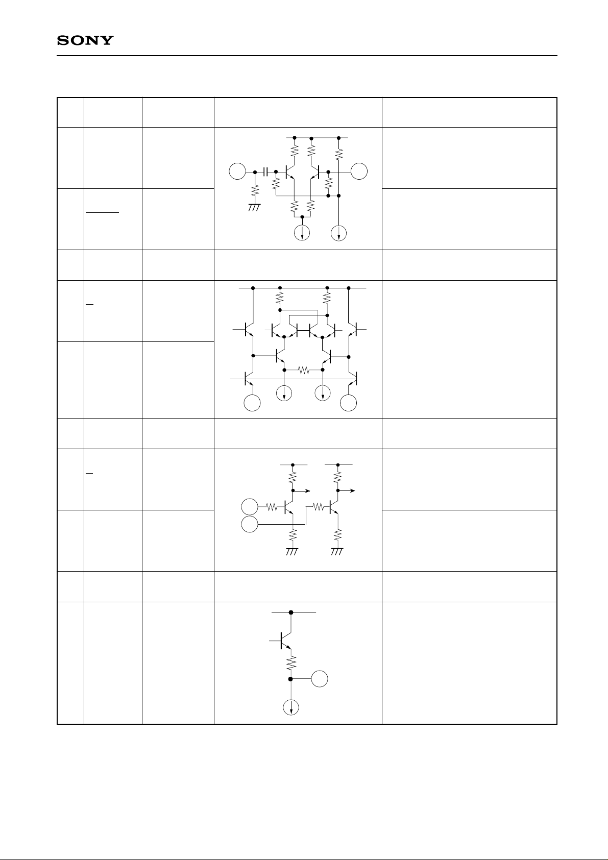
Local input pin. The internal resistor
1 2
provides 50 Ω matching.
Bias pin for the local input amplifier.
Ground this pin via a capacitor.
Local leak level adjustment pins.
Normally ground these pins via 1 kΩ
resistors.
6
GND
7
Q-INPU
8
Q-INPUT
9
GND
10
IF OUTPUT
0
∗
1.85 V to
0.85 V
∗
1.85 V to
0.85 V
0
∗
1.4
45
Q signal input pin. The input
impedance is 500 kΩ or more.
(Only DC signals can be normally
7
8
input at the VCC/2 DC Bias.)
Q signal input pin. The input
impedance is 500kΩ or more.
(Signals of up to 1 Vp-p can be input
at the VCC/2 DC Bias.)
IF output pin. (An output impedance
of 50 Ω is provided by the emitter
10
follower.)
—2—

CXA1852N
Pin
No.
11
12
13
14
Symbol
VCC
POWER
SAVE
I-INPUT
I-INPUT
Typical
pin voltage (V)
5.5 to 2.7
0 to 5.5
∗
0.85
to
1.85
∗
0.85
to
1.85
Equivalent circuit Description
Power supply pin.
Power saving control pin.
OFF when VP/S≤1.0 V; ON when
12
VP/S≥1.8 V
I signal input pin. The input
impedance is 500 kΩ or more.
(Signals of up to 1 Vp-p can be input
13
14
at the VCC/2 DC Bias.)
I signal input pin. The input
impedance is 500 kΩ or more
(Only DC signals can be normally
input at the VCC/2 DC Bias.)
15
16
17
18
19
20
GND
I-BIAS
I-BIAS
GND
N.C
GND
∗
0.175
∗
0.175
—
0
Local leak level adjustment pin.
Normally ground this pin via a 1 kΩ
resistor.
16 17
0
0
—3—
 Loading...