

High-Speed Sample-and-Hold IC
For the availability of this product, please contact the sales office.
Description
The CXA1843Q is a bipolar IC designed to sampleand-hold video and various other signals with high
speed. It is ideal for video and other signal
conversions.
Features
• Maximum operating rate = 33MHz (min.)
• Low power consumption: 320mW
• S/H clock pulse generator circuit
• Built-in clock pulse generator for A/D converter
Applications
When used in combination of the CXA1844Q, the
CXA1843Q achieves A/D conversion.
Absolute Maximum Ratings (Ta = 25°C)
• Supply voltage VCC 7V
VEE –7 V
• Input voltage
(VIN pin) VIN VEE to AVCC + 0.3 V
(REFIN pin) VREFIN +1 to AVCC + 0.3 V
(CLKIN pin) VCLK GND – 0.5 to DVCC + 0.3 V
(REX 2, 3, 4 pins)
VREX2, 3, 4 GND to GND + 4 V
• Reference voltage
(REFFB pin) VREFFB VEE to +3 V
(REFOUT pin) VREFOUT VEE to AVCC + 0.3 V
• Output current
(REFFOUT pin) IREFOUT –1 to +1 mA
(SHOUT pin) ISHOUT –12 to +12 mA
(CLKOUT pin) IADC –1.5 to +1.5 mA
• Storage temperature
Tstg –65 to +150 °C
• Allowable power dissipation
PD 1.1 W
Structure
Bipolar silicon monolithic IC
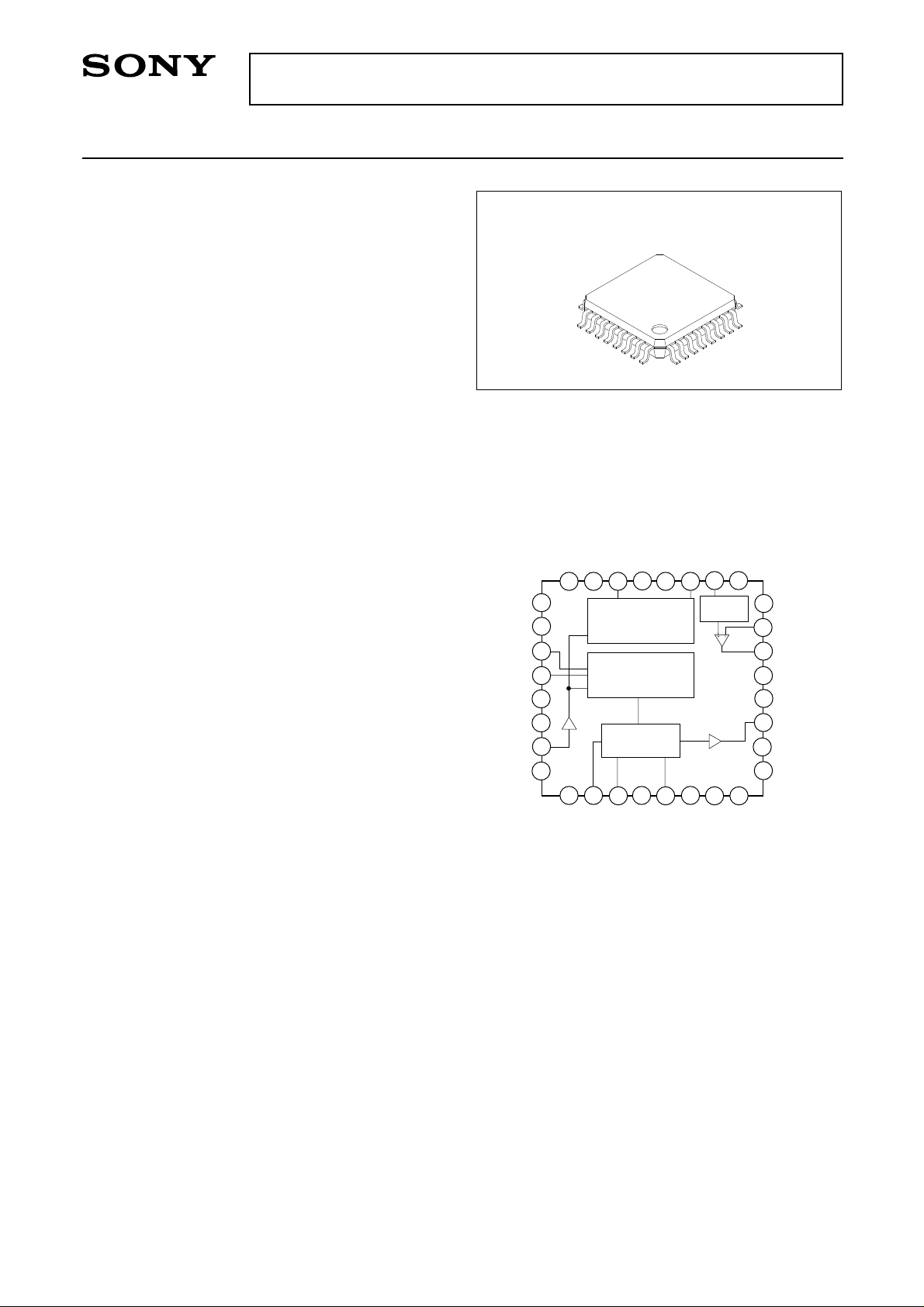
Block Diagram and Pin Configuration
NC
EE1
DV
REX3
REX4
DV
EE2
DV
CC3
CLK IN
NC
CXA1843Q
32 pin QFP (PIastic)
2
25
26
27
28
29
30
31
32
1
CC
CC
DV
DV
23
24
A/D CONVERTER
GENERATOR
SAMPLE HOLD
GENERATOR
1
2
1
CC
HGND
AV
CLKOUT
21
22
PULSE
PULSE
SAMPLE
HOLD
4
3
VIN
GND
1
EE
AV
NC
20
5
CGND
REX2
19
6
NC
REF IN
18
17
REF DC
SHIFT
7
8
NC
4
CC
AV
NC
16
15
14
13
12
11
10
9
NC
REFFB
REFOUT
AV
EE3
AV
CC3
SHOUT
EE2
AV
NC
Operating Conditions
• Supply voltage VCC 4.75 to 5.25 V
VEE –4.75 to –5.25 V
• Operating temperature
Topr –20 to +75 °C
Sony reserves the right to change products and specifications without prior notice. This information does not convey any license by
any implication or otherwise under any patents or other right. Application circuits shown, if any, are typical examples illustrating the
operation of the devices. Sony cannot assume responsibility for any problems arising out of the use of these circuits.
– 1 –
E92855B7Y
Pin Description
CXA1843Q
Pin
No.
1
2
3
4
Symbol
AVCC1
HGND
VIN
AVEE1
Pin voltage Equivalent circuit Description
5V (Typ.)
0V
—
–5V (Typ.)
HGND
VIN
DVEE2
AV
CC1
130
30k
Analog positive power supply.
Internal resistance GND for
sample-and-hold.
Sample-and-hold-input.
Analog negative power supply.
5
6
7
8
9
10
11
CGND
NC
NC
NC
NC
AVEE2
SHOUT
0V
—
—
—
—
–5V (Typ.)
AV
EE1
500µ 500µ
AVCC3
DVEE2
AVCC1
DVEE2
SHOUT
Internal capacitance GND for
sample-and-hold.
CGND
Connect to AGND.
Connect to AGND.
Connect to AGND.
Connect to AGND.
Analog negative power supply.
Sample-and-hold output.
– 2 –
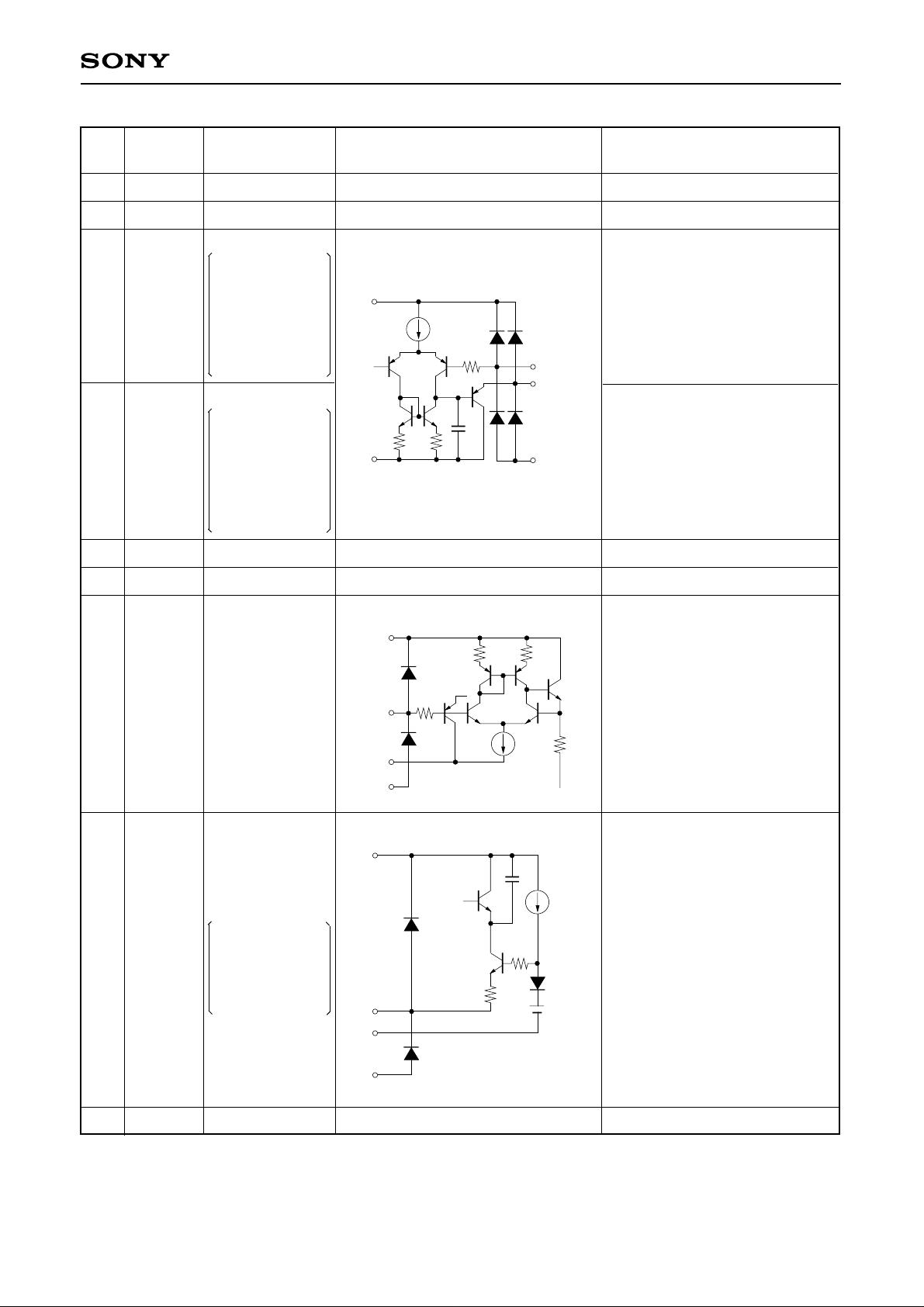
CXA1843Q
Pin
No.
12
13
14
15
16
17
Symbol
AVCC3
AVEE3
REFOUT
REFFB
NC
AVCC4
Pin voltage Equivalent circuit Description
5V (Typ.)
–5V (Typ.)
Analog positive power supply.
Analog negative power supply.
–2.8V
As shown in the
Application
Circuit, PNP TR.
is connected
and 2.5V is
applied to
AVCC4
400µ
130
REFFB
Connect the base of the
external PNP transistor to
create a –2V power supply.
Pin18.
–2V
REFOUT
As shown in the
Application
Circuit, PNP TR.
is connected
and 2.5V is
AVEE3
DV
EE2
Connect the emitter of the
external PNP transistor to
create a –2V power supply.
applied to
Pin18.
—
5V (Typ.)
Connect to AGND.
Analog positive power supply.
18
19
REFIN
REX2
2.5V (Typ.)
Approx. 0.5V
When external
resistor is
connected
between Pin 19
and AGND
AVCC4
REFIN
GND
DVEE2
DVCC2
REX2
GND
DV
EE2
130
300µ
1k
130
0.5V
External DC input for adjusting
the –2V power supply.
Connect external resistor that
determines the time interval (T2)
between master clock (MCLK)
rise and A/D converter clock
(A/D CLK) fall.
(Normally connect to 1.6kΩ)
20
NC
—
Connect to AGND.
– 3 –

CXA1843Q
Pin
No.
21
22
23
24
25
26
27
Symbol
GND
CLKOUT
DVCC1
DVCC2
NC
DVEE1
REX3
Pin voltage Equivalent circuit Description
0V
H:
DVCC2 – 0.78V
L:
DVCC2 – 1.52V
(Typ.)
5V (Typ.)
5V (Typ.)
—
–5V (Typ.)
Approx. 0.5V
When external
resistor is
connected
between Pin 27
and DGND
DV
GND
DVEE2
DV
CC2
600
CLKOUT
2.2mA
CC2
1k
GND
A/D converter clock (A/D CLK)
output.
Digital positive power supply.
Digital positive power supply.
Connect to DGND
Digital negative power supply.
Connect external resistor that
determines the time interval (T3)
between master clock (MCLK)
rise and sample-and-hold
internal clock (S/H CLK) rise.
(Normally connect 2.7kΩ)
28
29
30
31
32
REX4
DVEE2
DVCC3
CLKIN
NC
Approx. 0.5V
When external
resistor is
connected
between Pin 28
and DGND
–5V (Typ.)
5V (Typ.)
—
—
REX3
REX4
GND
DVEE2
CC3
DV
CLKIN
GND
DVEE2
130
130
300µ
130
1k
0.5V
Connect external resistor that
determines the time interval (T4)
between master clock (MCLK)
rise and sample-and-hold
internal clock (S/H CLK) rise.
(Normally connect 1.5kΩ)
Digital negative power supply.
Digital positive power supply.
Master clock (MCLK) input.
TTL level.
(Vth = 1.5V)
Connect to DGND.
– 4 –
CXA1843Q
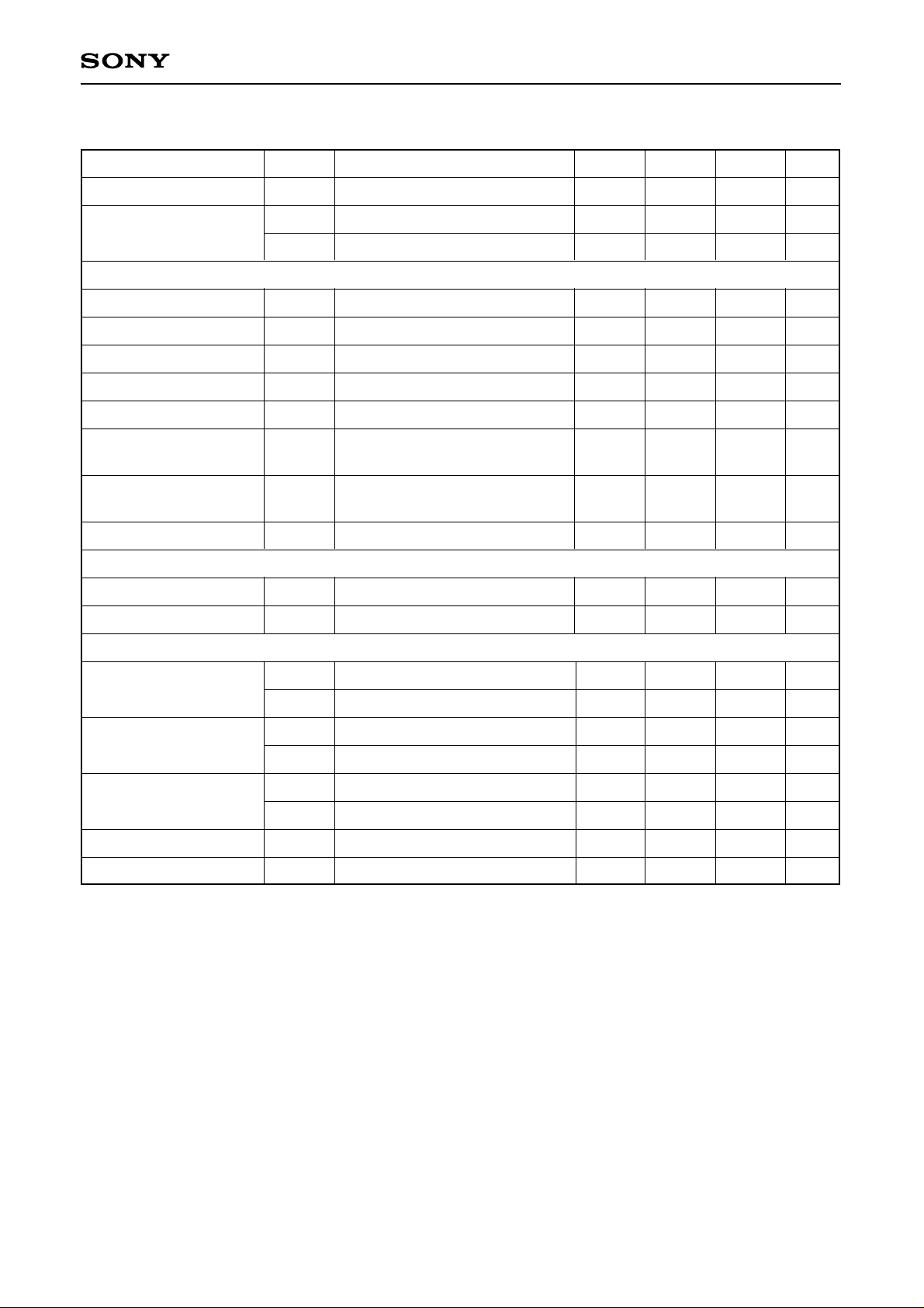
Electrical Characteristics (Ta = 25°C, VCC = 5V, VEE = –5V)
Item
Symbol
Maximun operating rate FC
ICC
Current consumption
IEE
S/H Amplifier Block
VIN input current
VIN input voltage range
Droop
Feed through
S/H output offset voltage
S/H output gain
S/H output frequency
response
S/H output slew rate
IVIN
VIN
HMDR
HMTH
VOFFSET
Gsh
Fsh
SR
Reference Amplifier Block
REFIN input current
IREFIN
Conditions
VIN = –1V
FIN = 1kHz, distortion factor ≤ –55dB
VIN = –2V to 0V
FIN = 16.5MHz (2Vp-p)
VIN = –1V, FCLK = 33MHz
FIN = 1kHz (2Vp-p),
FCLK = 33MHz
20Log (VO (16.5MHz)/VO (200kHz)),
Sampling time = 14ns
CL = 50pF
VREFIN = 2.5V
Min.
33
32
–28
1
–2.2
–20
–40
55
–0.5
–1
140
0
Typ.
41
–23
20
20
–50
90
0.3
0.2
160
1
Max.
Unit
MHz
50
–18
mA
mA
50 µA
0.2 V
80 mV/µs
–70 dB
120 mV
0.5 dB
1dB
200 V/µs
10 µA
REFFB output voltage
Digital I/O Block
CLKIN input current
CLKIN input voltage
CLKIN clock width
A/D clock low level
A/D clock high level
VREFFB
ICLKL
ICLKH
VCLKL
VCLKH
TPWH
TPWL
VADCL
VADCH
VREFIN = 2.5V
VCLKIN = 0V
VCLKIN = 5V
–2.2
–10
0
2.0
9
9
VCC – 0.90
–2.0
–6
0
VCC – 1.52
VCC – 0.78
–1.8 V
0µA
1µA
0.8 V
VCC – 1.40
V
ns
ns
V
V
– 5 –
CXA1843Q
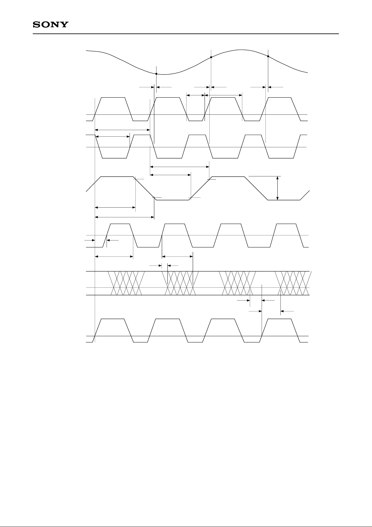
Timing Chart
VIN (Pin 3)
(0 to –2V)
MCLK(Pin 31)
(TTL)
S/H CLK
(Not output to outside)
S/H OUT (Pin 11)
(0 to –2V)
T3
Hold
N – 1
tdf
T4
taqf
Sample
Tsd
10%
N + 1
N
Tsd
T
Hold
tdr
90%
PWL
Sample
taqr
N
10%
TPWH
Hold
90%
N + 1
Sample
Tsd
N + 2
2Vp-p
Hold
Threshold
voltage =
1.5V
Threshold
voltage
N + 2
A/D CLK (Pin 22)
(PECL)
A/D output (CXA1844Q)
(TTL)
MCLK
(Clock pulse for the
device next to the ADC
in order to latch the
A/D output)
T1 =
6ns
DN – 3
T2
tD (min)
DN – 2
D (max)
t
DN – 1
DN
S
T
Th
Threshold
voltage =
CC – 1.2V
V
Threshold
voltage =
1.5V
Threshold
voltage =
1.5V
MCLK: System master clock.
S/H CLK: This clock actuates the internal sample-and-hold circuit.
The internal clock pulse circuit generates the S/H CLK, which is not output outside the IC.
A/D CLK: This clock actuates the A/D converter. The internal clock buffer circuit generates the A/D CLK.
This clock has the level where +5V is shifted from the ECL level.
TPWH, TPWL: S/H CLKIN input clock width
Tsd: S/H sampling delay for the S/H internal clock
T1: Fixed time interval between master clock rise and A/D CLK rise, T1 = 6ns (typ.)
T2: Time interval between MCLK rise and A/D CLK fall
T3: Time interval between MCLK rise and S/H CLK rise
T4: Time interval between MCLK rise and S/H CLK fall
taqf, tdf: 10%/90% falling output delay of S/H from MCLK rise
taqr, tdr: 10%/90% rising output delay of S/H from MCLK rise
tD (min., max.): Minimum/maximum output delay of A/D converter (Refer to the CXA1844Q specification.)
Ts: Setup time of A/D output and MCLK
Th: Hold time of A/D output and MCLK
– 6 –
 Loading...