

Sony CXA1829N Datasheet

CXA1829N
For the availability of this product, please contact the sales office.
8ch. Read/Write Amplifier for Thin Film Heads of Hard Disk Drive
Description
The CXA1829N is a Read/Write amplifier for hard
disk drive thin-film heads and is designed to handle
up to 8-channel heads.
Features
• Operates on a single 5V power supply.
• Low power consumption.
Read: 115 mW
Write (IW = 15 mA): 160 mW + IW × 5
Power Save: 7 mW
• Write current can be varied through an external
resistor. Built-in stabilizer circuit provides stable
current, preventing voltage and temperature drift.
• Drives up to 8 heads.
• Supports thin film heads or 2-pin MIG heads.
• Emitter follower-type Read amplifier features 290
times gain (typ.).
• Write-unsafe detection circuit.
• Damping resistance is switched at Write (315 Ω).
• Simultaneous Write function.
• Supply voltage monitor circuit prohibits error
writing during power surge or abnormal voltage.
• IC protection circuit for head-to-ground short circuit
protection.
• Differential input capacitance at Read: 14 pF (typ.).
• Write data input minimum pulse width: 10 ns
• Read data output in Write mode becomes a high
impedance due to the improved Read data offset
when Write is switched to Read.
• Non-selected head DC voltage falls to GND level.
Absolute Maximum Ratings (Ta=25°C)
• Supply voltage VCC 7.0 V
• Write current IW 20 mAo-p
• Operating temperature Topr –20 to +75 °C
• Operating temperature at Simultaneous Write
• Storage temperature Tstg –55 to +150 °C
• Allowable power dissipation
Recommended Operating Conditions
• Supply voltage VCC 5V±10% V
30 pin SSOP (Plastic)
Topr –20 to +30 °C
PD 480 mW
Structure
Bipolar silicon monolithic IC
Sony reserves the right to change products and specifications without prior notice. This information does not convey any license by
any implication or otherwise under any patents or other right. Application circuits shown, if any, are typical examples illustrating the
operation of the devices. Sony cannot assume responsibility for any problems arising out of the use of these circuits.
—1—
E94433A49-TE
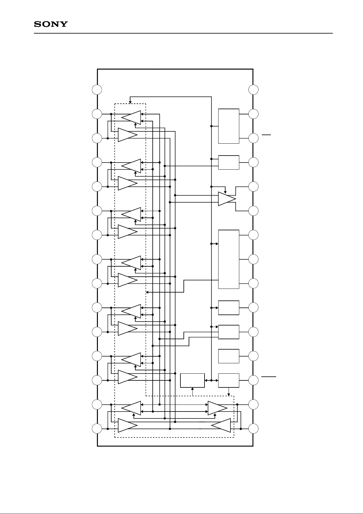
Block Diagram and Pin Configuration
CXA1829N
GND
H0X
H0Y
H1X
H1Y
H2X
H2Y
H3X
H3Y
30
29
28
27
26
GND
PS
R/W
WC
RDY
1
2
3
4
5
AMP
AMP
DRIVER
DRIVER
MODE
CONTROL
WRITE
CURRENT
SOURCE
AMP
6
7
DRIVER
AMP
25
24
RDX
HS0
HEAD
23
8
DRIVER
HS1
SELECT
9
AMP
22
HS2
POWER
DRIVER
ON/OFF
DETECTOR
T - FF
WRITE
UNSAFE
DETECTOR
WRITE
SERVO
AMP
10
H4X
11
H4Y
12
H5X
13
H5Y
14
H6X
15 16
H6Y
AMP
AMP
AMP
DRIVER
DRIVER
DRIVER
IC
PROTECTOR
21
20
19
18
17
V
CC
WDI
WUS
WSER
H7X
H7Y
—2—
Pin Description
No. Symbol Equivalent circuit Description
CXA1829N
1, 30 GND
2, 3 H0X, H0Y
4, 5 H1X, H1Y
6, 7 H2X, H2Y
8, 9 H3X, H3Y
10, 11 H4X, H4Y
12, 13 H5X, H5Y
14, 15 H6X, H6Y
16, 17 H7X, H7Y
19 WUS
20 WDI
GND connection.
Head input.
VCC
10
2
12
4
14
6
16
8
3
11
5
13
7
15
9
17
2k 2k
200k
330
330
GND
VCC
8 channels provided.
Write-unsafe detection output.
Open collector output. When it is
high in Write mode, an error is
19
GND
VCC
detected.
Write data input.
When high changes to low, input
is triggered.
21 VCC
22 HS2
23 HS1
24 HS0
28 R/W
29 PS
20
22
23
24
28
29
100k
2.1V
1.4V
2.1V
GND
2.1V
VCC
GND
VCC
GND
5 V power supply.
Head select signal input. Eight
heads are selected as shown in
Table 2.
Read/Write signal input.
Read at high; Write at low.
Power save signal input.
Power save at high.
—3—
No. Symbol Equivalent circuit Description
CXA1829N
18 WSER
25 RDX
26 RDY
27 WC
18
25
26
100k
2.1V
VCC
GND
VCC
GND
CC
V
Simultaneous Write signal input.
Set to low for simultaneous Write
mode.
Read amplifier output.
Becomes a high impedance at
Write.
A setting resistor for the Write
current value is connected
between this pin and GND.
27
1.25V
GND
—4—
CXA1829N
Electrical Characteristics (unless otherwise specified, VCC = 5 V, Ta = 25°C, Write current IW = 15 mA)
Refer to Measurement Circuit 1.
Item Symbol Measurement conditions ment Min. Typ. Max. Unit
Current consumption for
Read
Current consumption for
Write
Current consumption for
Servo
Current consumption for
Power save
I
IW
ISE
IP
R
R/W="H"
R/W="L"
WSER="L"
PS="H"
Measure-
point
E172333
E
E
24 32 45
W +IW +IW
+I
71 91 111
W +4×IW +4×IW
+4×I
E 0.8 1.4 2.0
mA
Digital low input voltage
Digital high input voltage
Digital low input current
Digital high input current
Write-unsafe output
saturation voltage
Write-unsafe output leak
current
Power ON/OFF detector
threshold voltage
Write current setting
range
Write current accuracy
Read amplifier differential
voltage gain
VIL
VIH
IL
IH
VWUS
IWUS
VTH
IW
∆Iw
AV
High applied voltage: 5 V
Low applied voltage: 0 V
Output current: 1 mA
Current flowing between head pins.
When Write current is I
K
___
W=
Rw
(Rw:Ω),
I
W [mA], then:
Refer to Fig. 12 (Characteristics) for K.
Input voltage SG1:1mVp-p,300kHz
Load resistance (RDX, RDY): 1kΩ
B 0.8
DV
F 2.0
G
H -70
IµA
J70
C 0.5 V
C10µA
CC
V
3.6 3.9 4.3 V
A
A 5 15 mAo-p
A-8 8%
K 245 290 335 V/V
Bandwidth (-3 dB)
Input conversion noise
voltage
Common mode rejection
ratio
BW
EN
CMRR
Frequency at which Av drops by 3dB
Head impedance: 0 Ω
In-phase input voltage SG2:100mVp-p,
10 MHz
—5—
K 60 MHz
K 0.55 0.7
nV
√Hz
K5077 dB
 Loading...