Sony CXA1821M Datasheet

RF Amplifier for CD Players
Description
The CXA1821M is an IC developed for compact
disc players. This IC incorporates an APC circuit and
RF, focus error, and tracking error amplifiers for 3spot optical pickup output. (The voltage-converted
optical pickup output is supported.)
Features
• Low power consumption (40mW at ±2.5V)
• APC circuit
• Both single power supply (+5V) and dual power
supply (±2.5V) operations possible.
• Compatible with pickup for LC and PD
• Supports the RF amplifier at double speed.
Applications
Compact disc players
Structure
Bipolar silicon monolithic IC
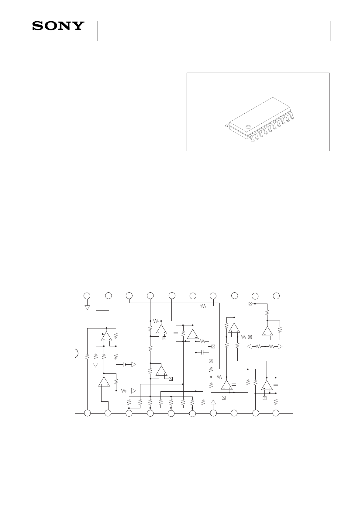
Block Diagram and Pin Configuration
Absolute Maximum Ratings (Ta = 25°C)
• Supply voltage VCC 12 V
• Operating temperature Topr –20 to +75 °C
• Storage temperature Tstg –65 to +150 °C
• Allowable power dissipation
PD 600 mW
Operating Conditions
• Supply voltage VCC – VEE 2.8 to 11.0 V
– 1 –
E94932-TE
Sony reserves the right to change products and specifications without prior notice. This information does not convey any license by
any implication or otherwise under any patents or other right. Application circuits shown, if any, are typical examples illustrating the
operation of the devices. Sony cannot assume responsibility for any problems arising out of the use of these circuits.
CXA1821M
20 pin SOP (Plastic)
LD
PD
A
B
C
D
V
EE
F
E
EI
V
CC
VCC
LD ON
LC/PD
RFE
RFO
FE
FE BIAS
TE
VC
EO
1k
56k
10k
55k
56k
10k
VEE
10k
VEE
VREF
1.25V
APC LD AMP
24k
30k
24k
30k
24k
24k
30k
30k
28k
5.6k
10k
RF EQ AMP
22k
V
C
VC
RF SUMMING AMP
174k
25p
164k
FOCUS
ERROR AMP
87k
25p
V
EE
26k
13k
12p
23.8k
23.8k
123k
820k
12p
VCC
30k
VEE
147
VC
VC
VC
260k
123k
260k
VC BUFFER
15k
VC
VC
30k
TRACKING
ERROR AMP
V
CC
820k
VC
2
3
4
5
6
7
8
9
10
11
12
13
14
15
16
17
18
19
20
1

– 2 –
CXA1821M
1
2
3
4
5
6
14
7
LD
PD
A
B
C
D
FE BIAS
VEE
O
I
I
I
I
I
I
—
1k
10k
55.7k
VCCVCC
VEE
1
55k
V
EE
147
17µ
VEE
10k
V
EE VEE
VCC
2
4.9k
28k
VEE
24k
30k
24k
30k
24k
30k
24k
30k
100µ
87k
174k
VEE
8µ
25p
25p
FE BIAS
164k
A
B
C
D
V
CC
VCC
VCC VCC
VC
VC
3
4
5
6
14
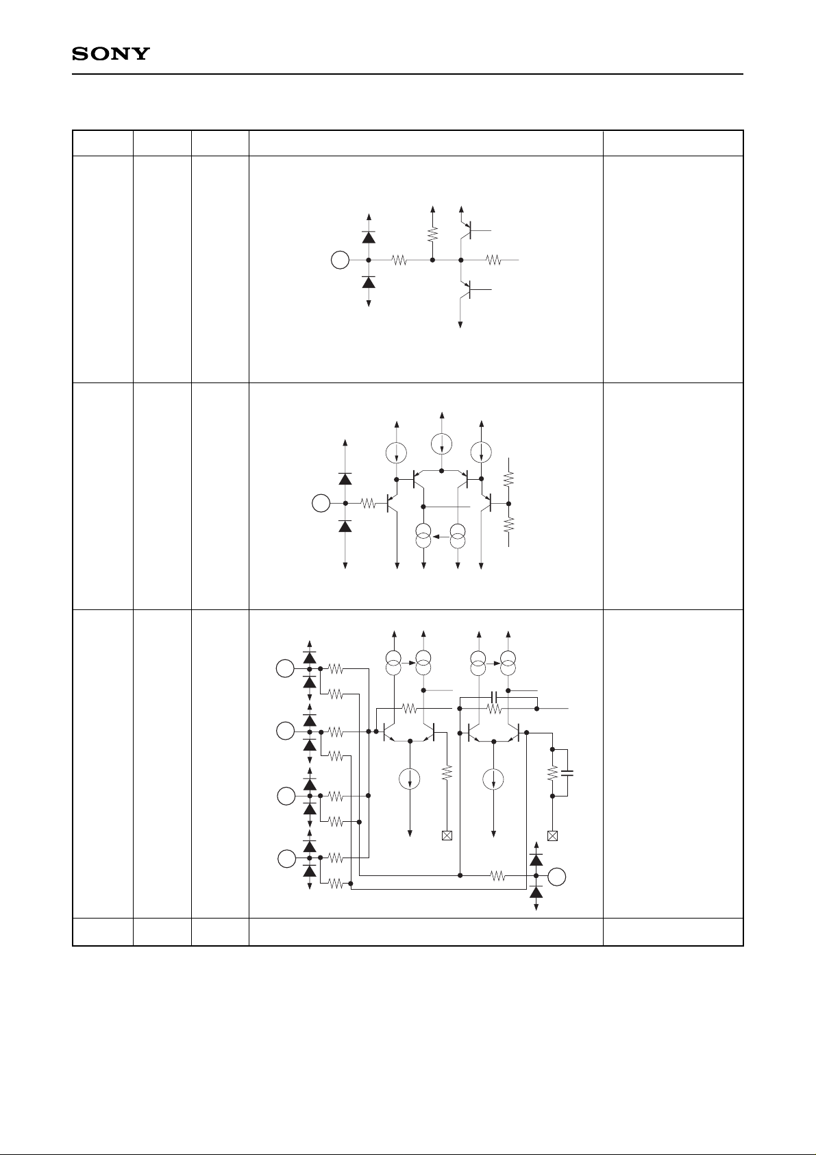
Output pin of APC
amplifier.
Input pin of APC
amplifier.
Input pin of RF and
FE amplifier for Pins
3, 4, 5 and 6; focus
bias adjustment for
Pin 14.
VEE.
Pin No. Symbol I/O Equivalent circuit Description
Pin Description

– 3 –
CXA1821M
8
9
10
11
18
12
13
15
F
E
EI
EO
LC/PD
VC
TE
FE
I
I
—
—
I
O
O
O
96.3k
VEE
147
260k
VC
VCC
8µ
12p
820k
820k
260k
147
23.8k
96.3k
V
EE
VC
8µ
12p
VCC
VCC
VCC
VCC
8µ 300µ
VCC
147
8
9
10
11
18
120
V
EE
VCC
147
200µ
120
16k
15k
VCC
12
10p
VEE
147
400µ
123k
VEE
VCC
13
VCC
10p
VEE
147
400µ
174k
VEE
25p
15
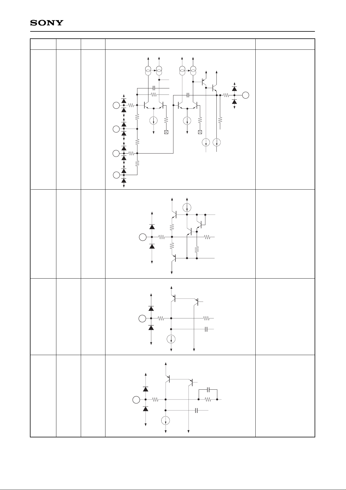
Input pin of tracking
error amplifier for
Pins 8 and 9. An
external resistor for
V-I conversion
should be connected
because these pins
are for current input.
Gain adjustment of
input signal from Pin
9 for Pins 10 and 11.
Pin 18 is a bias for
LC when connected
to VCC and for PD IC
when left open.
DC voltage output
pin of (VCC + VEE)/2.
Connect to GND
when dual power
supply (±2.5V) is
used; connect a
smoothing capacitor
when single power
supply (+5V) is used.
Output pin of
tracking error
amplifier. The F-E
signal is output.
Output pin of focus
error amplifier.
Pin No. Symbol I/O Equivalent circuit Description

– 4 –
CXA1821M
16
17
19
20
RFO
RFE
LD ON
VCC
O
—
I
—
147
22k
VCC
VEE
16
7.3k
5.6k
VEE
200µ
10k
22k
VC
17
30k
VEE
VCC
147
50µ
VEE
VEE
VEE
VREF
19
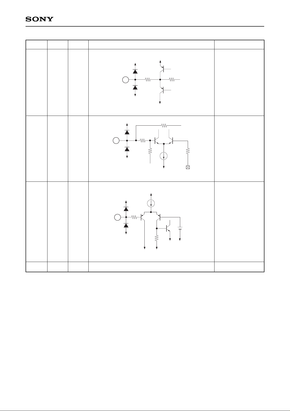
Output pin of RF
amplifier.
Equalizing pin is
used of RF amplifier.
Frequency response
can be adjusted by
connecting CR to
this pin.
ON/OFF selection
pin of APC amplifier.
ON for VCC and OFF
for VEE
VCC.
Pin No. Symbol I/O Equivalent circuit Description
 Loading...