

Sony CXA1819Q Datasheet

RGB Driver for LCD
Description
The CXA1819Q is an RGB driver designed for
LCD panel LCX007. It supports a line alternative
RGB drive system. In addition, three-panel
projectors can be supported by using three
CXA1819Q ICs.
Features
• Built-in RGB signal phase matching sample-and-
hold circuit
• Effective frequency response (horizontal resolution
of 600 TV lines achieved in combination with the
LCX007AL)
• Built-in γ control circuit
• Built-in side black generation circuit for 4:3/16:9
aspect conversion
• Built-in VCOM voltage output circuit
CXA1819Q
48 pin QFP (Plastic)
Structure
Bipolar silicon monolithic IC
Applications
Liquid crystal projectors
Liquid crystal viewfinders
Compact liquid crystal monitors
Absolute Maximum Ratings
• Supply voltage VCC 14 V
• Operating temperature Topr –20 to +75 °C
• Storage temperature Tstg –65 to +150 °C
• Allowable power dissipation
PD 600 mW
Operating Condition
Supply voltage VCC15 V
VCC2 12.2 to 13.3 V
Sony reserves the right to change products and specifications without prior notice. This information does not convey any license by
any implication or otherwise under any patents or other right. Application circuits shown, if any, are typical examples illustrating the
operation of the devices. Sony cannot assume responsibility for any problems arising out of the use of these circuits.
– 1 –
E94634A77
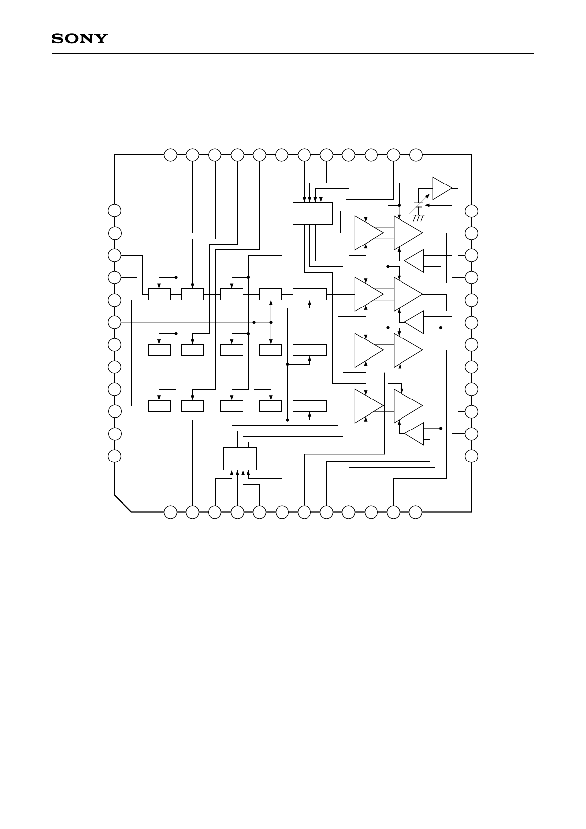
Block Diagram
CXA1819Q
NC
NC
RIN
GIN
BIN
BRT
CC1
V
CC1
V
GND1
GND1
SH1
NC
BF
35
36
34
SH2
32
33
37
SH4
SH3
31
BBRT
30
29
SUB BRT
CONT
38
RBRT
RGBBRT
SIDBRT
26
27
28
AMP
39
40
41
CLP GAMMAS/H BRT
S/H
AMP
42
43
CLP
S/H S/H
GAMMABRT
44
45
46
CLP GAMMABRT
S/H S/H
PRG
BUFF
BUFF
BUFFAMP
BUFFAMP
FRP
25
24
NC
23
VCOMCONT
22
VCOMOUT
21
SIDCLP
20
SIDOUT
19
CC2
V
18
CC2
V
17
GND2
16
GND2
15
ROUT
MODE
NC
47
48
2
NC
GAMMA
GAIN
CONT
4
3
7
6
5
9
8
10
121
11
NC
BCLP
BGAIN
RGAIN
RGBGAIN
SIG.C
SIDGAIN
GCLP
BOUT
GOUT
14
RCLP
13
NC
– 2 –

Pin Description
CXA1819Q
Pin
No.
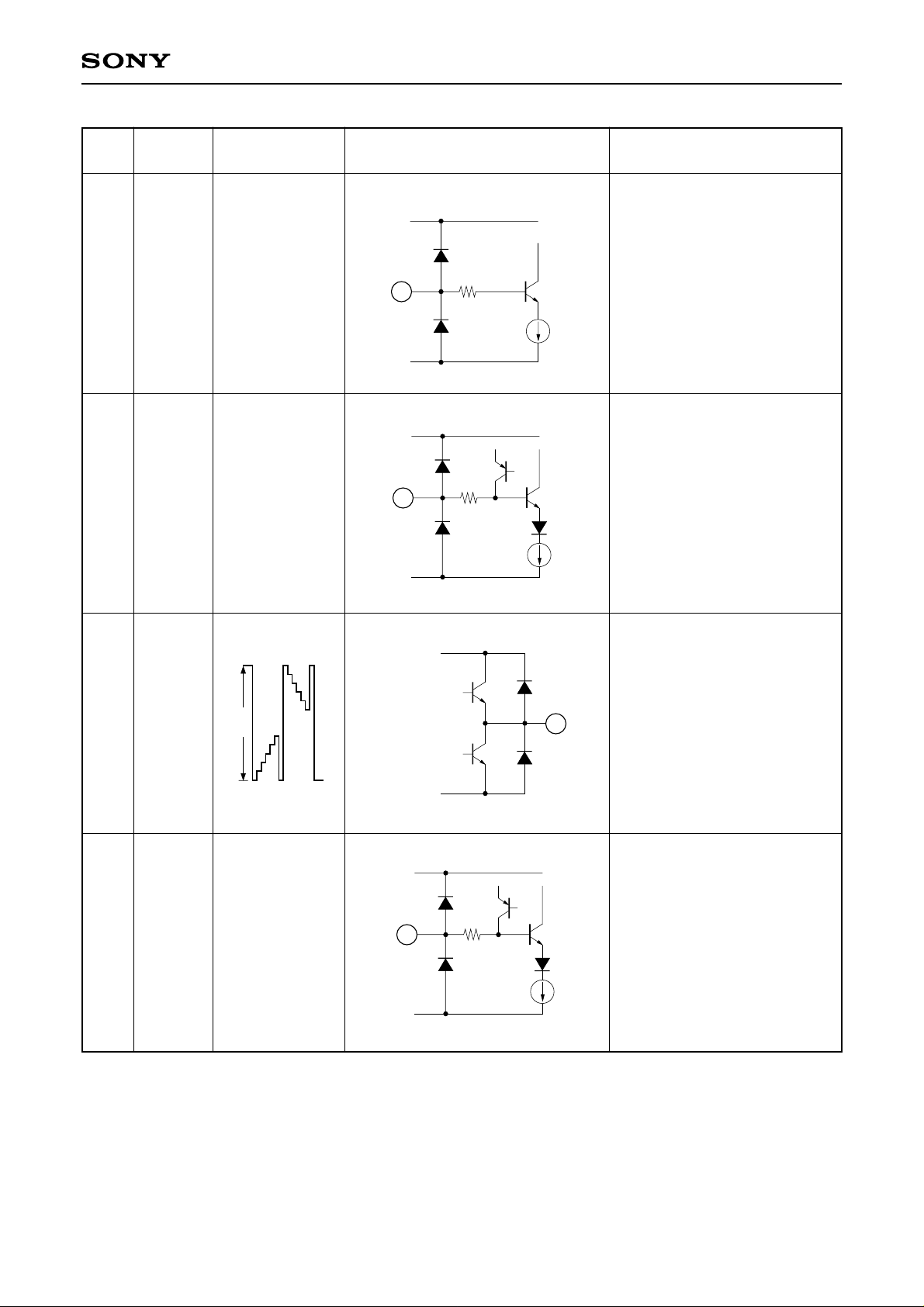
Symbol Pin voltage Equivalent circuit Description
2 GAMMA
3 B GAIN
4 R GAIN
0 to 5V
1.6 to 5V
1.6 to 5V
VCC1
1.5k
∗
2
129
50µA
GND1
VCC1
∗
1.5k
3
4
∗
GND1
129
50µA
Gamma control.
Gamma variable range:
3.7 to 15dB
Preset mode (pin 0V) ≈ 0dB
B signal gain control.
Gain variable range:
–2.0 to +2.0dB
R signal gain control.
Gain variable range:
–2.0 to +2.0dB
VCC1
RGB
5
GAIN
SID
6
GAIN
1.6 to 5V
1.6 to 5V
∗
∗
5
129
GND1
VCC1
6
129
GND1
Note)∗in the Pin voltage indicates external applied voltage.
400
RGB signal common gain
control.
Gain variable range: 5.5 to 11dB
150µA
1.5k
SID signal gray level control.
50µA
– 3 –
CXA1819Q
Pin
No.
7
8
Symbol Pin voltage Equivalent circuit Description
VCC2
RGB signal center voltage
SIG
CENT
B CLP
1.6 to 5V
6.2 to 7.6V
∗
7
GND1
VCC2
∗
8
GND1
129
100µA
129
5µA
control.
Center voltage variable range:
6.2 to 7.6V
B output detection signal input.
VCC2
B signal output.
9 B OUT
8V
Typ.
9
The output is fed back to
provide sufficiently low
impedance (less than few Ω).
GND2
VCC2
10 G CLP G output detection signal input.
6.2 to 7.6V
∗
10
GND1
129
5µA
Note)∗in the Pin voltage indicates external applied voltage.
– 4 –
CXA1819Q
Pin
No.
Symbol Pin voltage Equivalent circuit Description
11 G OUT
R CLP
14
8V
Typ.
6.2 to 7.6V
VCC2
G signal output.
11
The output is fed back to
provide sufficiently low
impedance (less than few Ω).
GND2
VCC2
∗
14
GND1
129
5µA
R output detection signal input.
15 R OUT
16
GND2
17
18
Vcc2 13V
19
20
SID OUT
8V
Typ.
Typ.
8V
GND
VCC2
GND2
VCC2
R signal output.
15
The output is fed back to
provide sufficiently low
impedance (less than few Ω).
GND.
13V power supply.
SID signal output.
20
The output is fed back to
provide sufficiently low
impedance (less than few Ω).
GND2
Note)∗in the Pin voltage indicates external applied voltage.
– 5 –

CXA1819Q
Pin
No.
Symbol Pin voltage Equivalent circuit Description
21 SID CLP
VCOM
22
OUT
6.2 to 7.6V
6.2 to 8.0V
VCC2
∗
21
GND1
VCC2
129
5µA
SID output detection signal
input.
VCOM voltage output.
The output is fed back to
22
provide sufficiently low
impedance (less than few Ω).
50µA
GND1
VCC2
VCOM
23
CONT
25 FRP
1.6 to 5V
30µs
H
L0V
∗
5V
23
129
GND1
VCC2
25
129
GND1
Note)∗in the Pin voltage indicates external applied voltage.
100µA
100µA
2.5V
VCOM voltage control.
VCOM voltage variable range:
6.2 to 8.0V
Flyback pulse input.
This pulse is used to invert the
polarity of R, G and B outputs.
Input level: High ≥ 4V,
Low ≤ 1V
– 6 –
 Loading...