Sony CXA1814N Datasheet

8 mm VCR ATF
Description
The CXA1814N is an IC developed for ATF
(Automatic Track Finding) in 8 mm VCRs, and
integrates the major functions necessary for ATF
onto a single chip.
Features
• Built-in pilot signal detector and BPF
• Adopts a high-precision analog filter with no
switching noise
• Built-in SP/LP identification circuit and clog
detection circuit
• Low noise, high-precision bipolar process
Applications
ATF for 8 mm VCRs
CXA1814N
30 pin SSOP (Plastic)
Structure
Bipolar silicon monolithic IC
Pin Configuration (Top View)
PBIN
TEST
BPF16 OUT
BPF46 OUT
REF PILOT
3FH IN
FH IN
3FH-FH
VCC
NC
GND
NF
10
11
12
30
1
2
3
4
5
6
7
8
9
SPIN
29
COMP REF
28
ENV OUT
27
MOD RATIO
26
CLOG REF
25
CLOG
24
SP/LP REF
23
PB SP/LP
22
CS
21
SIN
20
SCLK
19
CLOCK IN
ATF ERROR
RPPB MODE
PILOT ACT
Sony reserves the right to change products and specifications without prior notice. This information does not convey any license by
any implication or otherwise under any patents or other right. Application circuits shown, if any, are typical examples illustrating the
operation of the devices. Sony cannot assume responsibility for any problems arising out of the use of these circuits.
13
14
15 16
– 1 –
18
VREF
17
STBY
REC PILOT
E95Y08A62-PP
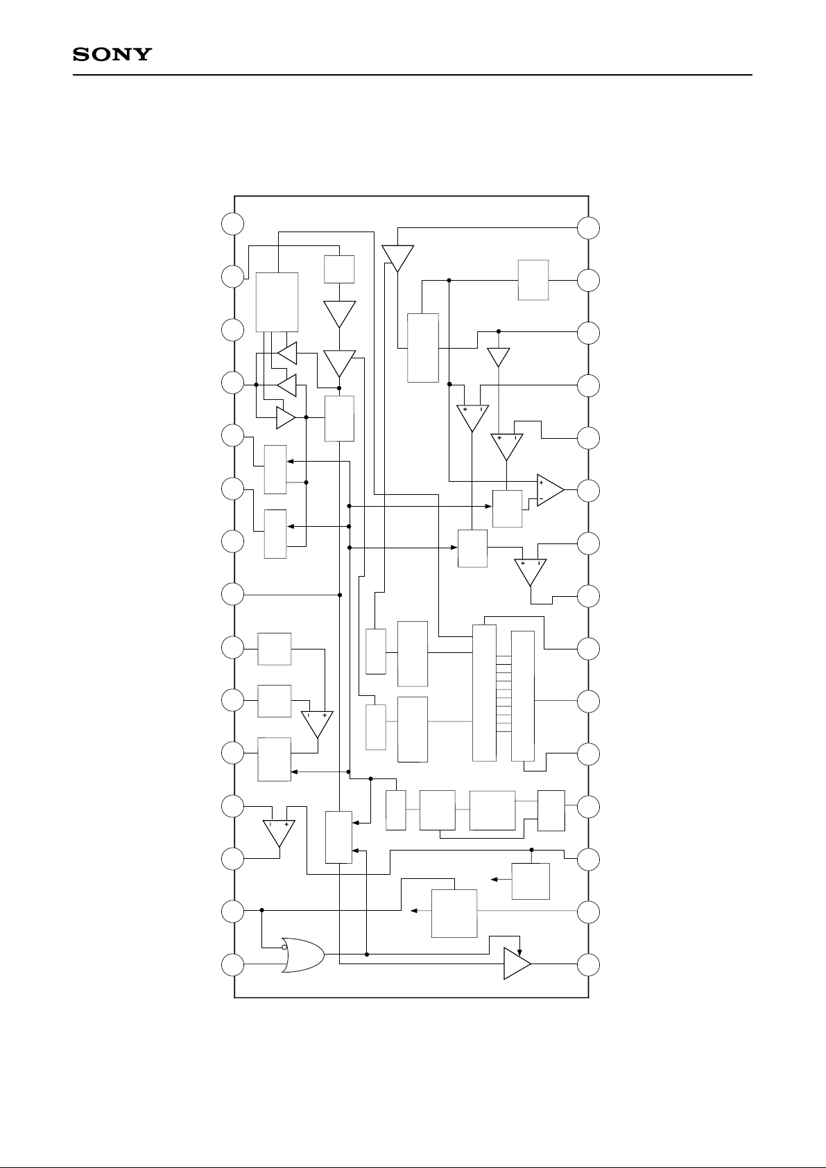
Block Diagram
CXA1814N
V
PBIN
NC
TEST
BPF16
OUT
BPF46
OUT
GND
REF
PILOT
3FH IN
1
CC
LPF
2
CONTROL
CIRCUIT
TEST
PB
24dB
GCA2
DETECTOR
ENVELOPE
0.55V
VREF
3
GCA1
4
BM
5
6
7
8
9
16KBPF
46KBPF
DET
3FH
V-I
D8 to D9
DECODER
4-16
D4 to D7
LPF
LPF
2.2Hz
10 BIT LATCH
33Hz
10BIT SHIFT REGISTER
30
29
28
27
26
25
24
23
22
SPIN
COMP
REF
ENV
OUT
MOD
RATIO
CLOG
REF
CLOG
SP/LP
REF
PB
SP/LP
CS
FH IN
3FH-FH
NF
ATF
ERROR
RPPB
MODE
PILOT
ACT
DET
LPF
FH
SUB
875HZ
RCLPF
10
11
12
13
14
15 16
V-I
DECODER
4-16
V-I
D0 to D3
BM
MODE
POWER
BPF
REF
185K
0°
90°
1.65V
VREF
1/2
5
21
20
19
18
17
SIN
SCLK
CLOCK
IN
VREF
STBY
REC
PILOT
– 2 –
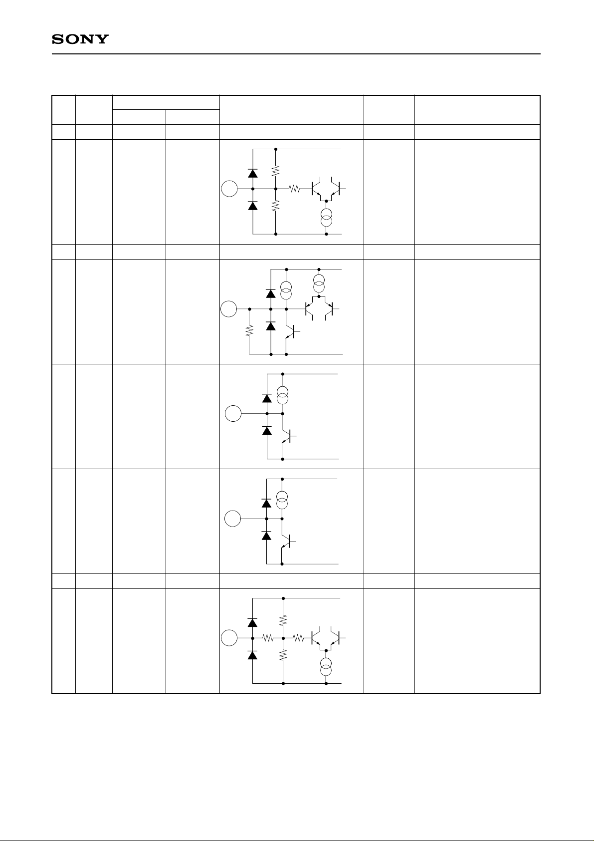
Pin Description
CXA1814N
Pin
Symbol
No. DC AC impedance
1
VCC
2
PBIN
3
NC
4
TEST
Pin voltage
3.15 V
1.77 V
typ
1.77 V for
output
1.58 V for
input
—
0.1 to 1.0
Vp-p
—
Approx.
0.5 Vp-p
Typ.
for output
0.5 Vp-p
or less
for input
Equivalent circuit
2
4
100k
85k
50k
120k
75µA
5µA
5µA
V
GND
VCC
GND
VCC
I/O
—
CC
50 kΩ
—
100 kΩ
Description
Power supply for all circuits.
Playback RF signal input.
Unconnected.
GCA1, BMIN and BMOUT
test I/O.
Pull up to VCC with a 100
kΩ resistor during signal
input.
5
6
7
8
BPF16
OUT
BPF46
OUT
GND
REF
PILOT
1.77 V
1.77 V
0 V
1.77 V
Approx.
0.5 Vp-p
Typ.
Approx.
0.5 Vp-p
Typ.
—
1.0 Vp-p
or less
50µA
5
GND
VCC
50µA
6
GND
—
V
CC
210k
15k
8
50k
130 kΩ
270k
5µA
GND
BPF16K output.
BPF46K output.
GND for all circuits.
Input for reference pilot
signal. Maximum input
level is 1 Vp-p.
– 3 –
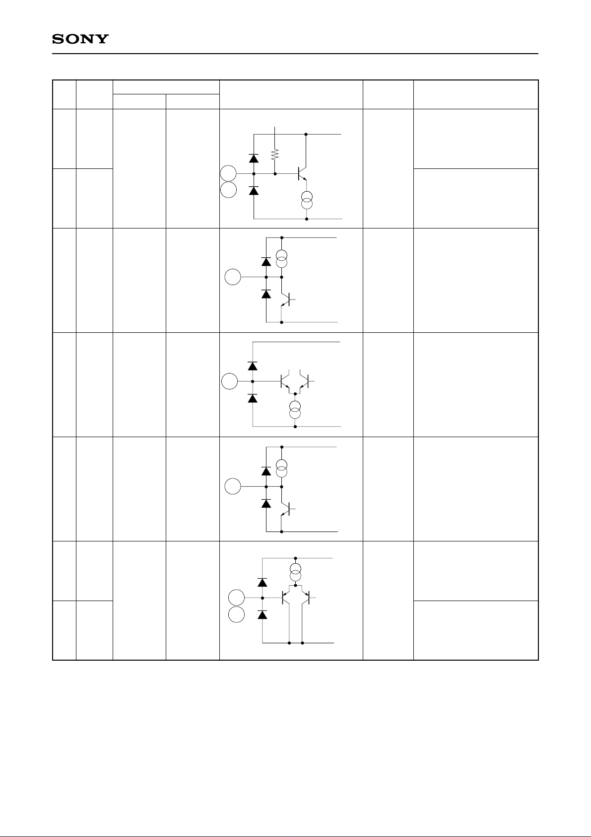
CXA1814N
Pin
Symbol
No. DC AC impedance
9
3FHIN
10
FHIN
3FH
11
-FH
12
NF
Pin voltage
1.58 V
1.58 V
1.58 V
1.0 Vp-p
or less
—
—
Equivalent circuit
9
10
11
12
VREF
60k
50µA
5µA
10µA
V
GND
VCC
GND
VCC
GND
I/O
CC
60 kΩ
Description
3FH signal input.
Connect it to Pin 6 with
capacitor coupled.
FH signal input.
Connect it to Pin 5 with
capacitor coupled.
FH detection circuit output.
Operational amplifier
inverted input for the FH
detection circuit output
amplifier.
13
14
15
ATF
ERROR
RPPB
MODE
PILOT
ACT
1.58 V
LOW≤0.8 V
HIGH≥2.1 V
—
—
13
14
15
50µA
5µA
VCC
GND
VCC
GND
Operational amplifier
output for the FH detection
circuit output amplifier.
Mode control.
High: Playback mode
Low: Recording mode
Pilot signal output control.
High: ENABLE
Low: DISABLE
– 4 –
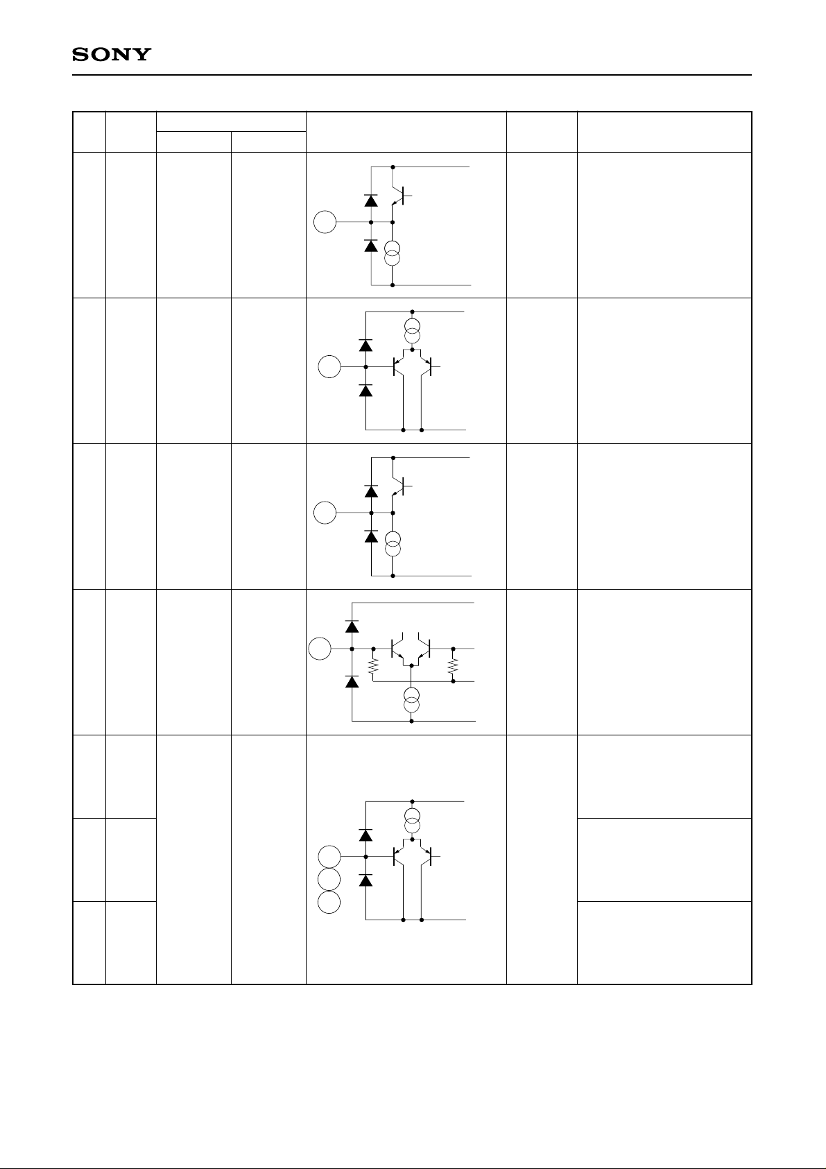
CXA1814N
Pin
Symbol
No. DC AC impedance
REC
16
PILOT
17
STBY
18
VREF
Pin voltage
1.10 V
LOW≤0.8 V
HIGH≥2.1 V
1.58 V
Approx.
0.5 Vp-p
—
—
Equivalent circuit
16
17
18
I/O
VCC
180µA
GND
VCC
5µA
GND
VCC
100µA
Description
Pilot signal output.
Power save mode control.
High: STBY
Electric potential for FH
detection operating point.
19
20
21
22
CLOCK
IN
SCLK
SIN
CS
VCC—0.7 V
LOW≤0.8 V
HIGH≥2.1 V
Approx.
0.3 Vp-p
Typ.
—
19
20
21
22
150k 150k
30µA
5µA
GND
V
GND
VCC
GND
CC
150 kΩ
External clock input.
Serial input clock for
GCA1 and GCA2 gain and
TEST mode control.
Serial data input for GCA1
and GCA2 gain and TEST
mode control.
Chip select input for GCA1
and GCA2 gain and TEST
mode control.
– 5 –
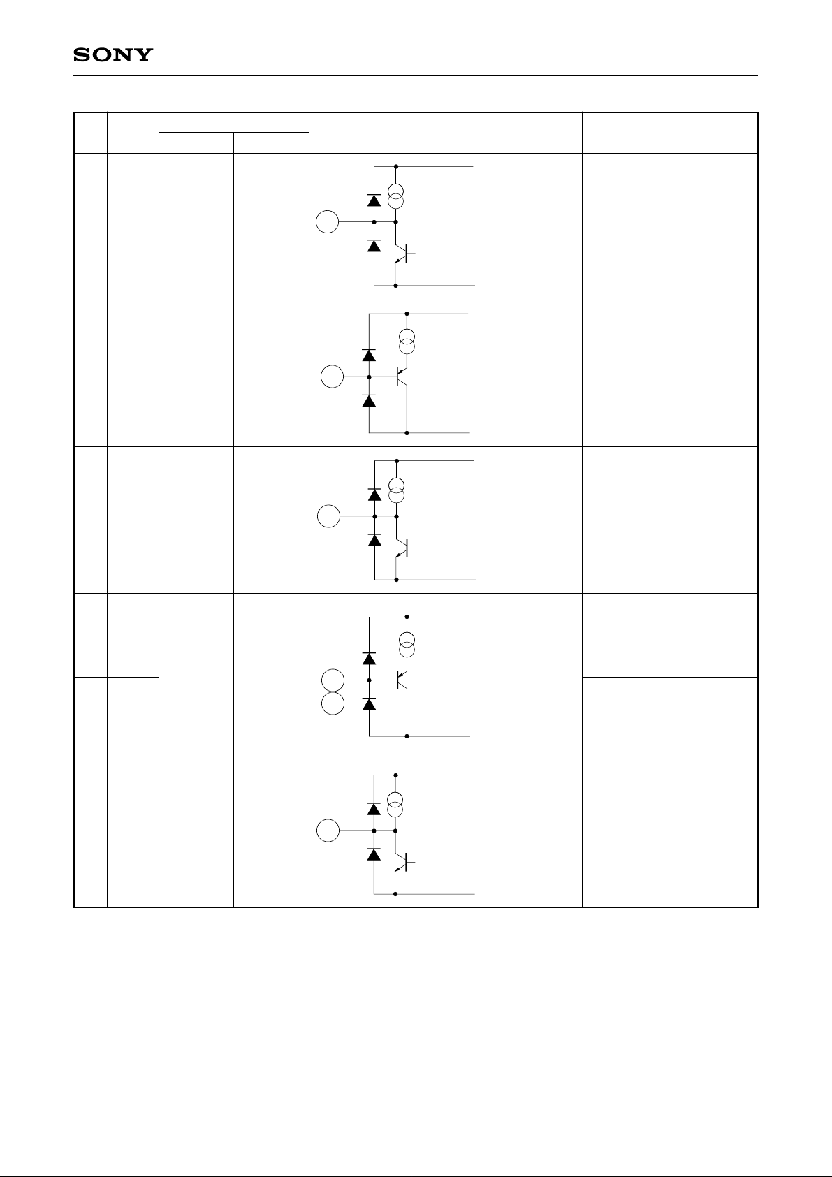
CXA1814N
Pin
Symbol
No. DC AC impedance
PB
23
SP/LP
SP/LP
24
REF
25
CLOG
Pin voltage
HIGH≥VCC
–0.8 V
LOW≤0.4V
0 V to VCC
–1.4 V
HIGH≥VCC
–0.8 V
—
—
—
Equivalent circuit
23
24
25
I/O
VCC
20µA
GND
VCC
5µA
GND
VCC
20µA
LOW≤0.4 V
Description
This pin is as follows during
variable speed playback.
During SP mode: High
During LP mode: Low
“Low” during normal
playback.
Threshold level setting for
LP/SP identification during
special playback.
Clog detection output.
Clogged state: High
Normal state: Low
26
27
28
CLOG
REF
MOD
RATIO
ENV
OUT
0 V to VCC
–1.4 V
0.53 V
—
—
28
26
27
5µA
100µA
GND
VCC
GND
VCC
GND
Threshold level setting for
clog detection.
Input for DC shifted
envelope signal.
Envelope detector output.
– 6 –
 Loading...