

Sony CXA1812Q Datasheet

—1—
E93701A79-TE
Sony reserves the right to change products and specifications without prior notice. This information does not convey any license by
any implication or otherwise under any patents or other right. Application circuits shown, if any, are typical examples illustrating the
operation of the devices. Sony cannot assume responsibility for any problems arising out of the use of these circuits.
Absolute Maximum Ratings (Ta=25 °C)
• Supply voltage VCC 7V
•Operating temperature Topr –20 to +75 °C
• Storage temperature Tstg –65 to +150 °C
• Allowable power dissipation
PD 450 mW
Operating Conditions
• Supply voltage VCC 4.75 V
• Supply voltage range VCC 4.5 to 5.25 V
Description
The CXA1812Q is an IC developed for processing
video I/O signals in VCRs. This IC has a built-in
video output circuit designed especially for use with
viewfinders (VF), making this IC optimal for use in
camcorders. In addition, both the video input
system and the viewfinder video output system
provide title insertion functions, making it possible to
insert characters and graphics into video signals.
Features
• Built-in video output circuit for use with viewfinders
(title insertion function (white or black character),
compatible with SY/C and composite video output)
• Built-in C system EE/PB switch
EE : Electric-Electric monitor mode
• Title insertion function (white or black character)
• C MUTE function for playback in PAL mode
(Outputs C signal used for generating the
composite video signal)
• Built-in switch for switching between the two input
systems, Y and C
• Built-in 75 Ω driver for the two input systems, Y
and C
(with power saving function)
Structure
Bipolar silicon monolithic IC
S-terminal Compatible Video I/O
32 pin QFP (Plastic)
CXA1812Q
—2—
CXA1812Q
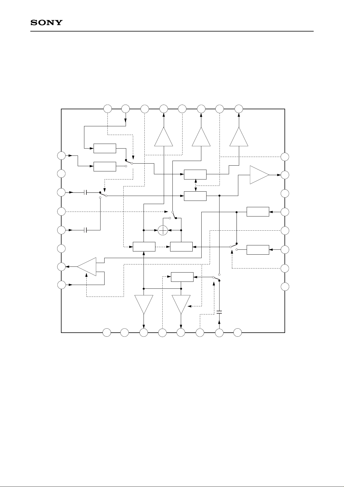
Block Diagram and Pin Configuration
23
24
1
2 3
4
5
6
7
8
9
10
11
12
13
14
15
16
17
1819
20
21
22
25
30
31
32
26
27
28
29
BUFF
BUFF
BUFF
6dB
12dB
DDS1
MUTE1
MUTE2
MUTE3
CLAMP
CLAMP
CLAMP
CLAMP
DDS2
DRIV
DRIV
YIN2
GND
CIN1
CIN2
Y/VSEL
YOUTGND
YOUT
YINVIN
VOB
COUT1
VCC
YIN
P.SAVE
EVFYIN
SEL1
YOUTV
CC
INSEL
YIN1
VOB1
EVFCOUT
VOW1
EVFY/VOUT
VOW
YOUT1
COUTGND
VREG
COUT2
CMUTE
COUT
SEL2
CIN
COUTVCC
—3—
CXA1812Q
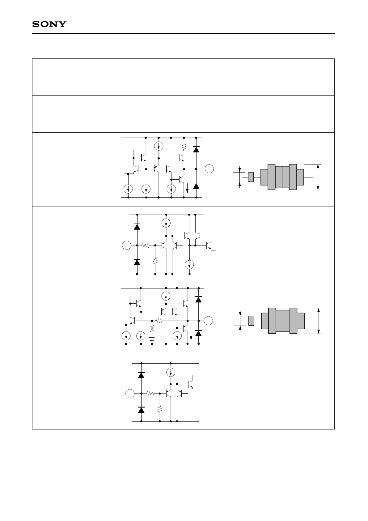
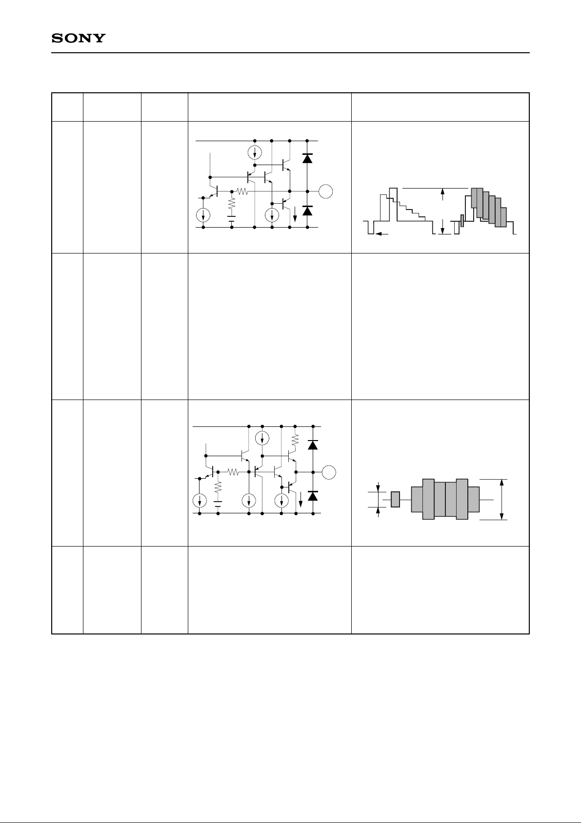
Pin Description ∗Externally applied voltage
Pin
Symbol
Pin
Equivalent circuit Description
No. voltage
1
2
3
4
5
6
COUTGND
VREG
COUT2
CMUTE
COUT
SEL2
0 V∗
4 V
2.2 V
0 V
2.2 V
0 V
3
60µ
150µ
120µ
GND
200
VCC
20µ
72k
150
GND
V
CC
4
GND
V
CC
660µ
660µ
16k
1.2m
2.2V
5.3k
5
GND
V
CC
20µ
150
72k
6
Chroma 75 Ω driver GND.
4 V internal regular output.
Connect a decoupling capacitor.
Do not use for external bias.
Chroma signal output used for
generating a composite video signal.
Control input used for muting both the
chroma signals that are input to Pins 27
(CIN1) and 29 (CIN2) and pass through
the EE path, as well as the chroma
signal that is input from Pin 7 (CIN).
Low (0 to 0.8 V) : normal operation
High (2 V to VCC) : mute
Chroma 75 Ω driver output.
Control input used for switching
between the signals input to Pins 27
and 29 and the signal input to Pin 7.
Low (0 to 0.8 V) :
signal at Pin 7 is selected
High (2 V to VCC) :
signals at Pins 27 and 29 are selected
314mVp-p143mVp-p
1.256Vp-p572mVp-p
—
—
∗Externally applied voltage
—4—
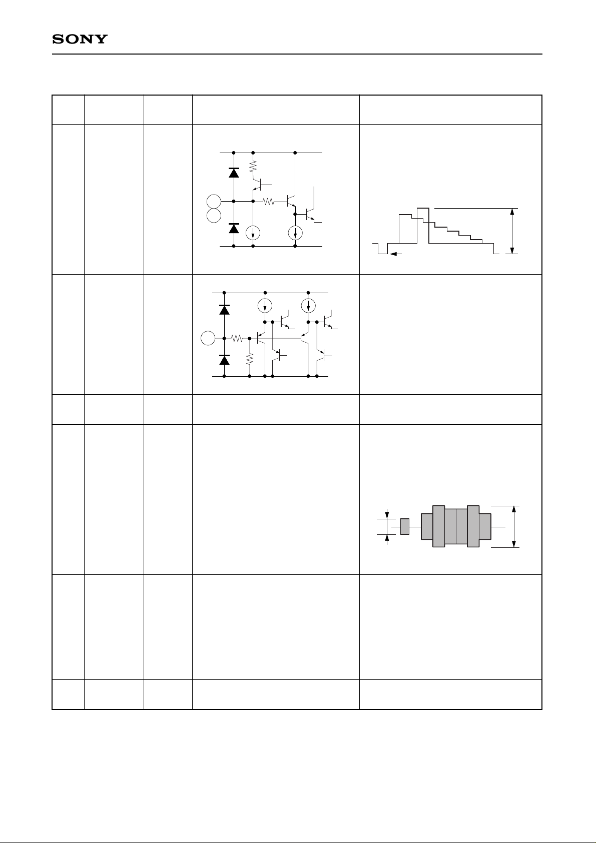
CXA1812Q
Pin
Symbol
Pin
Equivalent circuit Description
No. voltage
7
8
9
10
11
12
CIN
COUTVCC
YOUTVCC
SEL1
EVFYIN
P. SAVE
—
4.75 V∗
4.75 V∗
0 V
2.5 V
(Sync tip)
0 V
50k
80µ
150 20p
2.2V
7
GND
V
CC
1µ
50µ
200
1100
GND
V
CC
11
72k
15k
20µ
150
GND
V
CC
12
Video output chroma signal input.
Coupled by means of a capacitor within
the IC.
Inputting a signal of –0.3 V or less may
lead waveform distortion.
Chroma 75 Ω driver power supply.
Y 75 Ω driver power supply.
Control input used for switching the
signals that are input from Pins 11
(EVFYIN) and 13 (YIN).
Low (0 to 0.8 V) :
signal at Pin 13 is selected
High (2 V to VCC) :
signal at Pin 11 is selected
Y signal input for viewfinder.
Coupled by means of a capacitor ; in
order to keep clamp error to a
minimum, keep the input impedance as
low as possible.
Control input for power saver. When in
power saving mode, the Y and C 75 Ω
drivers stop operating. The output of
Pin 31 (YOUT) and Pin 5 (COUT) goes
to high impedance.
Low (0 to 0.8 V) : normal operation
High (2 V to VCC) : power saving mode
314mVp-p143mVp-p
0.5Vp-p
2.5V
—
—
Same as for Pin 6.
∗Externally applied voltage
—5—
CXA1812Q
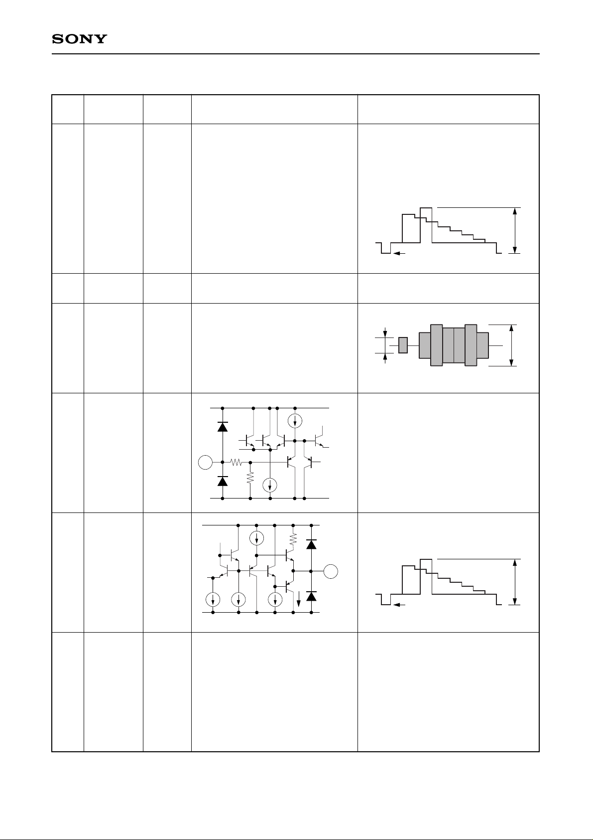
Pin
Symbol
Pin
Equivalent circuit Description
No. voltage
13
14
15
16
17
18
YIN
VCC
COUT1
VOB
YOUT1
VOW
2.5 V
(Sync tip)
4.75 V∗
2.2 V
0 V
1.8 V
(Sync tip)
0 V
72k
20µ
150
GND
V
CC
16
90µ
180µ
200
GND
V
CC
250µ
17
Video output Y signal input.
Coupled by means of a capacitor; in
order to keep clamp error to a
minimum, keep the input impedance as
low as possible.
Power supply other than the 75 Ω
driver.
Video input chroma signal output.
Control input for black level insertion of
the Y signals input to Pins 23 (YIN1)
and 25 (YIN2). The chroma signals
input from Pins 27 and 29 are also
muted simultaneously.
Low (0 to 0.8 V) : normal operation
High (2 V to VCC) : insertion mode
Video input Y signal output.
Control input for white level insertion of
the Y signals input to Pins 23 and 25.
The chroma signals input from Pins 27
and 29 are also muted simultaneously.
This pin takes precedence over the Pin
16 control signal.
Low (0 to 0.8V) : normal operation
High (2 V to Vcc) : insertion mode
0.5Vp-p
2.5V
314mVp-p143mVp-p
0.5Vp-p
1.8V
—
Same as for Pin 3.
Same as for Pin 4.
Same as for Pin 11.
—6—
CXA1812Q
∗Externally applied voltage
Pin
Symbol
Pin
Equivalent circuit Description
No. voltage
19
20
21
22
EVFY/VOUT
VOW1
EVFCOUT
VOB1
1.8 V
(Sync tip)
0 V
2.2 V
0 V
19
180µ
360µ 800µ
16k
GND
V
CC
2.1V
5.3k
21
200
GND
V
CC
2.2V
20k
20k
200µ
100µ
300µ
Y and composite video signal output for
the viewfinder. A composite video
signal is output when Pin 28 (Y/VSEL)
is high.
Control input for white level insertion of
the Y and composite video signals for
the viewfinder (output from Pin 19).
The chroma signal for the viewfinder
output from Pin 21 (EVFCOUT) is also
muted simultaneously. This pin takes
precedence over the Pin 22 (VOB1)
control signal.
Low (0 to 0.8 V) : normal operation
High (2 V to VCC) : insertion mode
Chroma signal output for the
viewfinder. When Pin 28 is high, the
output amplifier goes into power saving
mode and Pin 21 goes to high
impedance.
Control input for black level insertion of
the Y and composite video signals for
the viewfinder. The chroma signal for
the viewfinder is also muted.
Low (0 to 0.8 V) : normal operation
High (2 V to VCC) : insertion mode
1.8V
1Vp-p
628mVp-p286mVp-p
Same as for Pin 4.
Same as for Pin 6.
—7—
CXA1812Q
∗Externally applied voltage
Pin
Symbol
Pin
Equivalent circuit Description
No. voltage
23
25
24
26
27
29
28
30
YIN1
YIN2
INSEL
GND
CIN1
CIN2
Y/VSEL
YOUTGND
2.5 V
(Sync tip)
0 V
0 V∗
—
0 V
0 V∗
1100
GND
V
CC
200
1µ 40µ
23
25
72k
150
GND
V
CC
20µ 20µ
24
Video input Y signal inputs. Coupled
by means of a capacitor; in order to
keep clamp error to a minimum, keep
the input impedance as low as
possible.
Control input for switching between
signals input from Pins 23 and 25 and
from Pins 27 and 29.
Low (0 to 0.8 V) :
signals at Pins 23 and 27 are selected
High (2 V to VCC) :
signals at Pins 25 and 29 are selected
GND other than the 75 Ω driver.
Video input chroma signal inputs.
Coupled by means of a capacitor within
the IC.
Inputting a signal of –0.3 V or less may
lead waveform distortion.
Control input for switching the output
signal format for Pin 19.
Pin 19 output Pin 21 output
Low : Y signal Chroma signal
High : Composite High impedance
video signal
Low (0 to 0.8 V) High (2 V to VCC)
Y 75 Ω driver GND.
0.5Vp-p
2.5V
314mVp-p143mVp-p
Same as for Pin 7.
—
—
Same as for Pin 6.
 Loading...