

Sony CXA1810AR, CXA1810AQ Datasheet

—1—
E94X24-TE
Sony reserves the right to change products and specifications without prior notice. This information does not convey any license by
any implication or otherwise under any patents or other right. Application circuits shown, if any, are typical examples illustrating the
operation of the devices. Sony cannot assume responsibility for any problems arising out of the use of these circuits.
Absolute Maximum Ratings (Ta=25 °C)
• Supply voltage VCC 7V
•Operating temperature Topr –10 to +75 °C
• Storage temperature Tstg –65 to +150 °C
• allowable power dissipation
(when mounted on board)
PD CXA1810AQ 1050 mW
CXA1810AR 1010 mW
Operating Condition
Supply voltage VCC 4.75+0.5 to 4.75–0.25 V
Description
The CXA1810AQ/AR is an IC designed for 8mm
VCR Y/C main signal processing for consumer use.
Equipped with many built-in filters, the
CXA1810AQ/AR is a one-chip main signal
processing system that greatly reduces the number
of external components.
Features
• Built-in auto-adjusting filters
• Supports Hi-8 video.
• Supports camera recording.
• Supports power saving mode.
140 mW for composite signal input
250 mW for separate signal input
• Supports electronic volume (EVR) control.
• Supports BUS LINE.
• Supports NTSC/PAL.
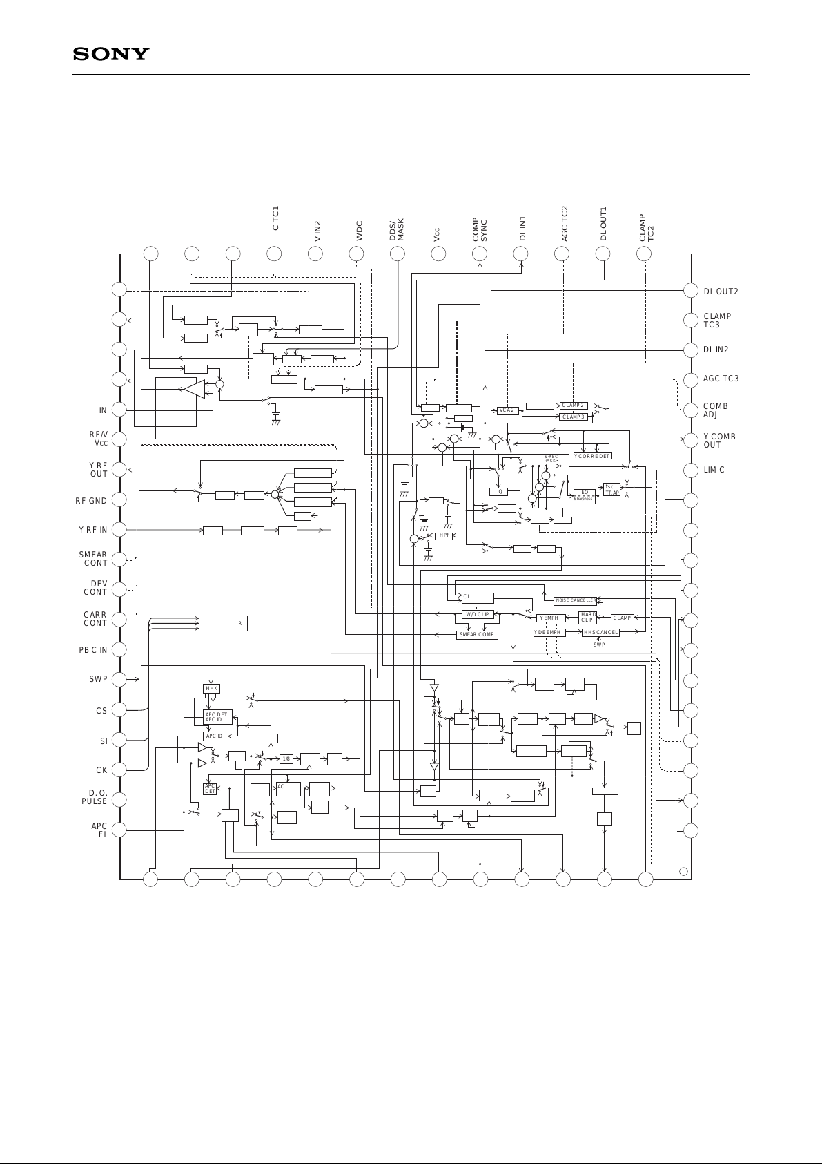
Functions
2-input INPUT SELECT, VIDEO AGC, DDS (Y
signal superimposition), synchronous separation, 75
Ω VIDEO OUT DRIVE, Y/C mixing, Y/C separation
comb filter, Y/C cross talk elimination, playback
chroma feedback comb, Y dropout compensation,
Yd playback switching, Y signal H correlation
detection, Y pre-emphasis/de-emphasis, white/dark
clipping, clipping compensation, MOD/DEMOD,
HHS/HHS cancel, ACC, chroma emphasis/deemphasis, burst emphasis/de-emphasis, XO/VXO,
APC, AFC, APC ID, AFC ID, burst ID, ACK, APC
compensation, HHK, PI/PS, frequency conversion
system, PB C BPF, REC C LPF, PB C LPF,
CARRIER BPF, 4.1 V regulator
Structure
Bipolar silicon monolithic IC
Luminance and Color Signal Processing for 8mm VCR
CXA1810AQ CXA1810AR
64 pin QFP (Plastic) 64 pin LQFP (Plastic)
CXA1810AQ/AR
—2—
CXA1810AQ/AR
Block Diagram and Pin Configuration
(CXA1810AQ)
S•REC
+ACK•REC
S•REC
+ACK•REC
BUS DECODER
HHK
AFC DET
AFC ID
APC ID
1/8
APC
DET
ACK BID
DET
ACK
CONT
ACK
BID
FF
fo
AUTO
CAR
CONV
1/N
CAR
BPF
VXO
XO
VCO
BF
CXA1810AQ
SWP
CAR. CONT
DEV. CONT
SMEAR. CONT
HHS
LPFDEMODLIM
LIM MOD
SYNC SEP
CLAMP
CLAMP
CLAMP
CLAMP
VIDEO
AGC
AGC DET
VD/HD
INSERT
Y MUTE
DDS
DOC TRAP
VCA 1
CLAMP 1
SYNC
ATT
ATT BPF
ATT
LIM
TRAP
EQ
EQ
fsc
TRAP
VCA 2
CLAMP 2
CLAMP 3
Sharpness
HPF
Y CORRE DET
NOISE CAN CELLER
W/D CLIP
SMEAR COMP
Y EMPH
Y DE EMPH
CLAMP
HARD
CLIP
HHS CANCEL
SWP
CLIP COMP
PI
PS
REC C
LPF
REC
CONV
BURST
EMPH
BURST
DEEMPH
CROMA
EMPH
ACC
AMP
CAR
INV
PB C
LPF
PB
CONV
PB C
BPF
ACC
CONT
ACC
DET
CROMA
DEEMPH
SWP
ACK
SW
SWP
ACK
SW
C MUTE
INSEL
AGC OFF
ON
PB
S•REC+PB
REC
TEST2
REC
TEST2
TEST1
REC
PB
REC
PB
CAM REC
TEST1
REC
PB
TEST1
REC
PB
REC
PB
C SEL
REC
PB
REC
PB
S•REC
PB
EDIT
PB•ACK
NO CORR
S•REC
W•PB
PB
W•PB
DOP
W•PB
Yd PB
PB
Yd PB
PB
REC
REC
W•PB
PB
REC
SHP
THROU
E
PB+REC CORR
REC•(S+443+EDIT+NO CORR)
+
+
+
—
+
–
+
–
+ +
+
+
+ –
–
+
+
+
+
+
A
A
A
A
A
A
A
A
A
A
A
A
A
A
1
2
3
4
5
6
7
8
9
10
11
12
13
14
15
16
17
18
19
20212223242526272829303132
33
34
35
36
37
38
39
40
41
42
43
44
45
46
47
48
49
50
51
52 53 54 55 56 57 58 59 60 61 62 63 64
CLAMP
TC1
Y OUT
V OUT
GND
VIDEO
OUT
INV IN
RF/V
VCC
Y RF
OUT
RF GND
Y RF IN
SMEAR
CONT
DEV
CONT
CARR
CONT
PB C IN
SWP
CS
SI
CK
D. O.
PULSE
APC
FL
Y IN
REC L/
JVD
V IN1
AGC TC1
V IN2
WDC
DDS/
MASK
V
CC
COMP
SYNC
DL IN1
AGC TC2
DL OUT1
CLAMP
TC2
DL OUT2
CLAMP
TC3
DL IN2
AGC TC3
COMB
ADJ
LIM C
Y COMB
OUT
C TRAP
VG1
DEEMPH
IN
COMP TC
REC
C OUT
DEMOD
OUT
NC TC IN
EMPH IN
SUB
EMPH TC
MAIN
EMPH TC
MAIN
EMPH OUT
C EMPH
CONT
AFC
FL
EXT
C IN
DC FB
I REF
GND
X TAL
IN
V REG
X TAL
OUT
CAM FSC
SHP
FSC
OUT
BF
VCO
C OUT
C IN
90°
SHIFT

—3—
CXA1810AQ/AR
Block Diagram and Pin Configuration
(CXA1810AR)
CROMA
EMPH
S•REC
+ACK•REC
BUS DECODER
HHK
AFC DET
AFC ID
APC ID
1/8
APC
DET
90°
SHIFT
ACK BID
DET
ACK
CONT
ACK
BID
FF
fo
AUTO
CAR
CONV
1/N
CAR
BPF
VXO
XO
VCO
BF
CXA1810AR
SWP
CAR. CONT
DEV. CONT
SMEAR. CONT
HHS
LPFDEMOD
LIM
LIM
MOD
SYNC SEP
CLAMP
CLAMP
CLAMP
CLAMP
VIDEO
AGC
AGC DET
VD/HD
INSERT
Y MUTE
DDS
DOC TRAP
VCA 1
CLAMP 1
SYNC
ATT
ATT
BPF
ATT
LIM
TRAP
EQ
EQ
fsc
TRAP
VCA 2
CLAMP 2
CLAMP 3
Sharpness
HPF
Y CORRE DET
NOISE CAN CELLER
W/D CLIP
SMEAR COMP
Y EMPH
Y DE EMPH
CLAMP
HARD
CLIP
HHS CANCEL
SWP
CLIP COMP
PI
PS
REC C
LPF
REC
CONV
BURST
EMPH
BURST
DEEMPH
ACC
AMP
CAR
INV
PB C
LPF
PB
CONV
PB C
BPF
ACC
DET
CROMA
DEEMPH
SWP
ACK
SW
SWP
ACK
SW
C MUTE
INSEL
AGC OFF
ON
PB
S•REC+PB
REC
TEST2
REC
TEST2
TEST1
REC
PB
CAM REC
TEST1
REC
PB
TEST1
REC
PB
REC
PB
C SEL
REC
PB
REC
PB
PB
EDIT
PB•ACK
NO CORR
S•REC
W•PB
PB
W•PB
DOP
W•PB
Yd PB
PB
S•REC
+ACK•REC
Yd PB
PB
REC
REC
W•PB
PB
REC
SHP
THROU
E
PB+REC CORR
REC•(S+443+EDIT+NO CORR)
ACC
CONT
REC
PB
S•REC
+
+
+
–
+
–
+ +
+
+
+
–
–+
+
+
+
+
+
49 50 51 52 53 54 55 56 57 58 59 60 61 62 63 64
1
2
3
4
5
6
7
8
9
10
11
12
13
14
15
16
17181920212223242526272829303132
33
34
35
36
37
38
39
40
41
42
43
44
45
46
47
48
Y IN
REC L/
JVD
V IN1
AGC TC1
V IN2
WDC
DDS/
MASK
V
CC
COMP
SYNC
DL IN1
AGC TC2
DL OUT1
CLAMP
TC2
DL OUT2
CLAMP
TC3
DL IN2
CLAMP TC1
Y OUT
V OUT GND
VIDEO OUT
INV IN
RF/V V
CC
Y RF OUT
RF GND
Y RF IN
SMEAR CONT
DEV CONT
CARR CONT
PB C IN
SWP
CS
SI
CK
D. O.
PULSE
APC
FL
AFC
FL
EXT
C IN
DC FB
I REF
GND
X TAL
IN
V REG
X TAL
OUT
CAM FSC
SHP
FSC
OUT
BF
VCO
C OUT
C IN
C TRAPC TRAP
AGC TC3
COMB ADJ
Y COMB OUT
LIM C
VG1
DEEMPH IN
COMP TC
REC C OUT
DEMOD OUT
NC TC IN
EMPH IN
SUB EMPH TC
MAIN EMPH TC
MAIN EMPH OUT
C EMPH CONT
—4—
CXA1810AQ/AR
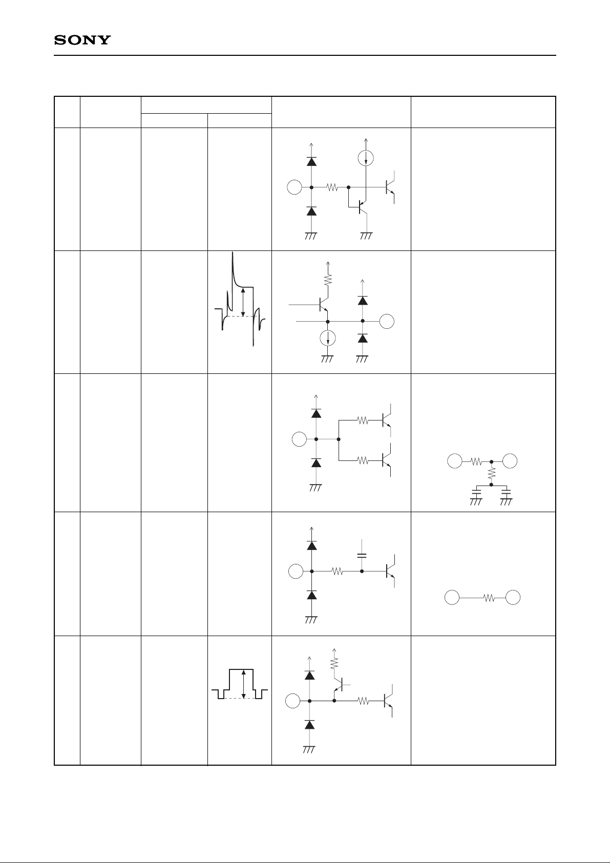
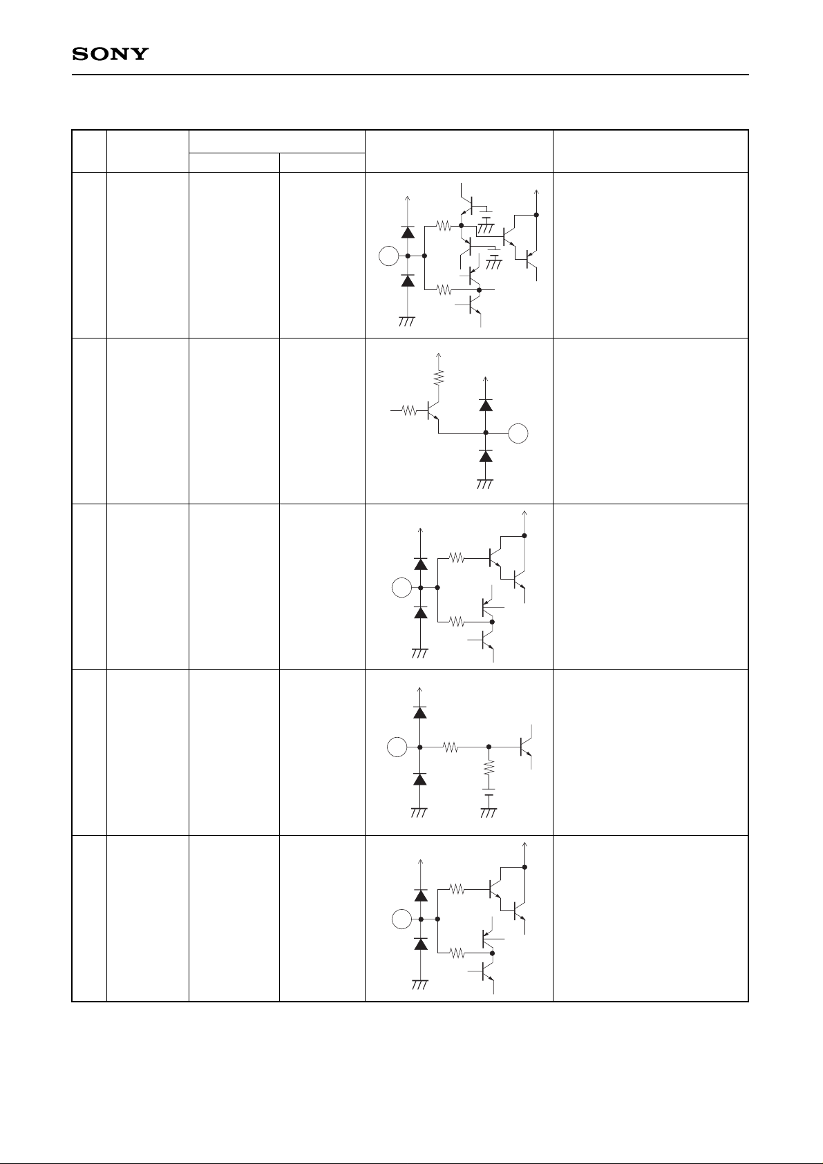
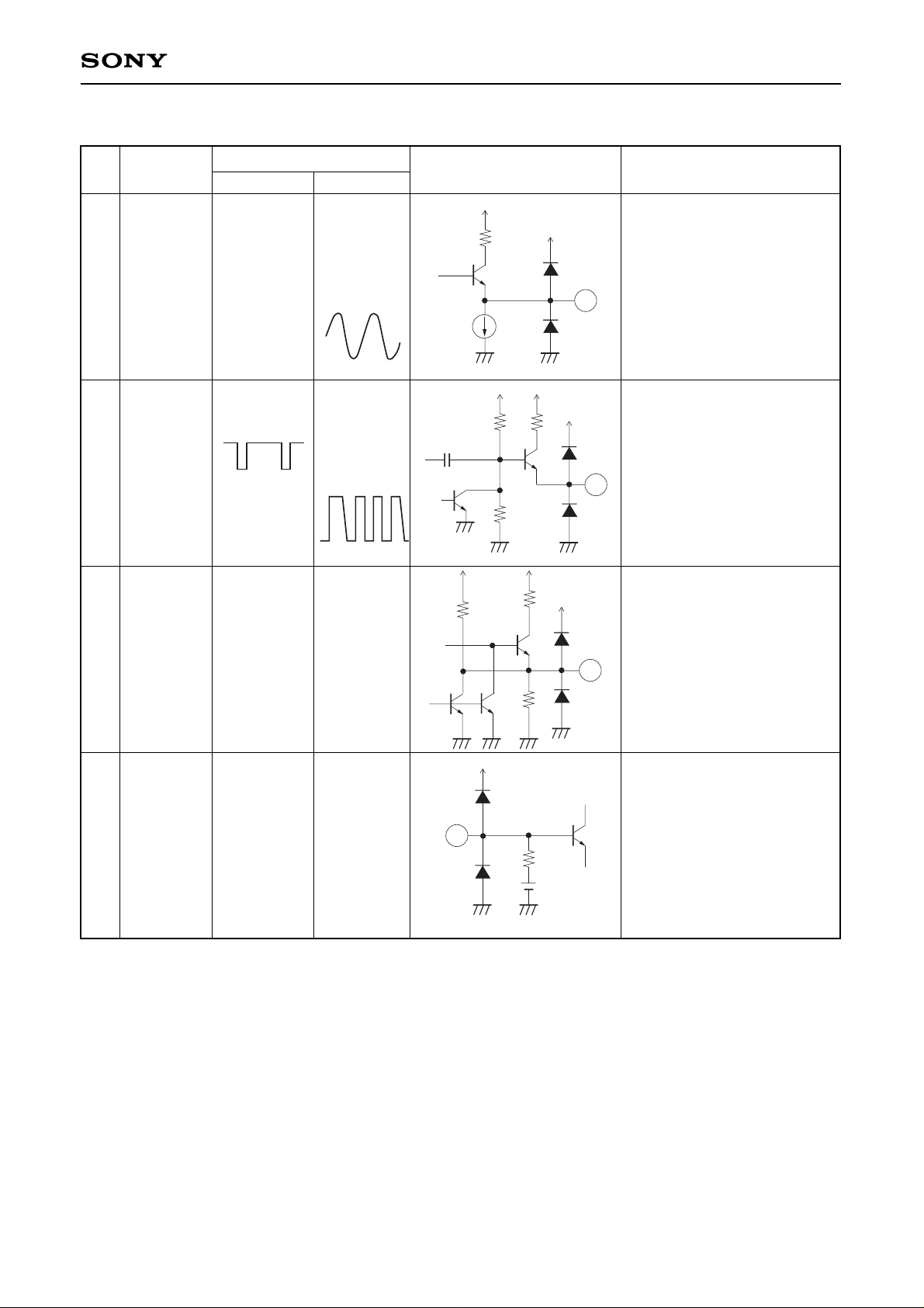
Pin Description
Pin
Symbol
Pin voltage
Equivalent circuit Description
No. DC AC
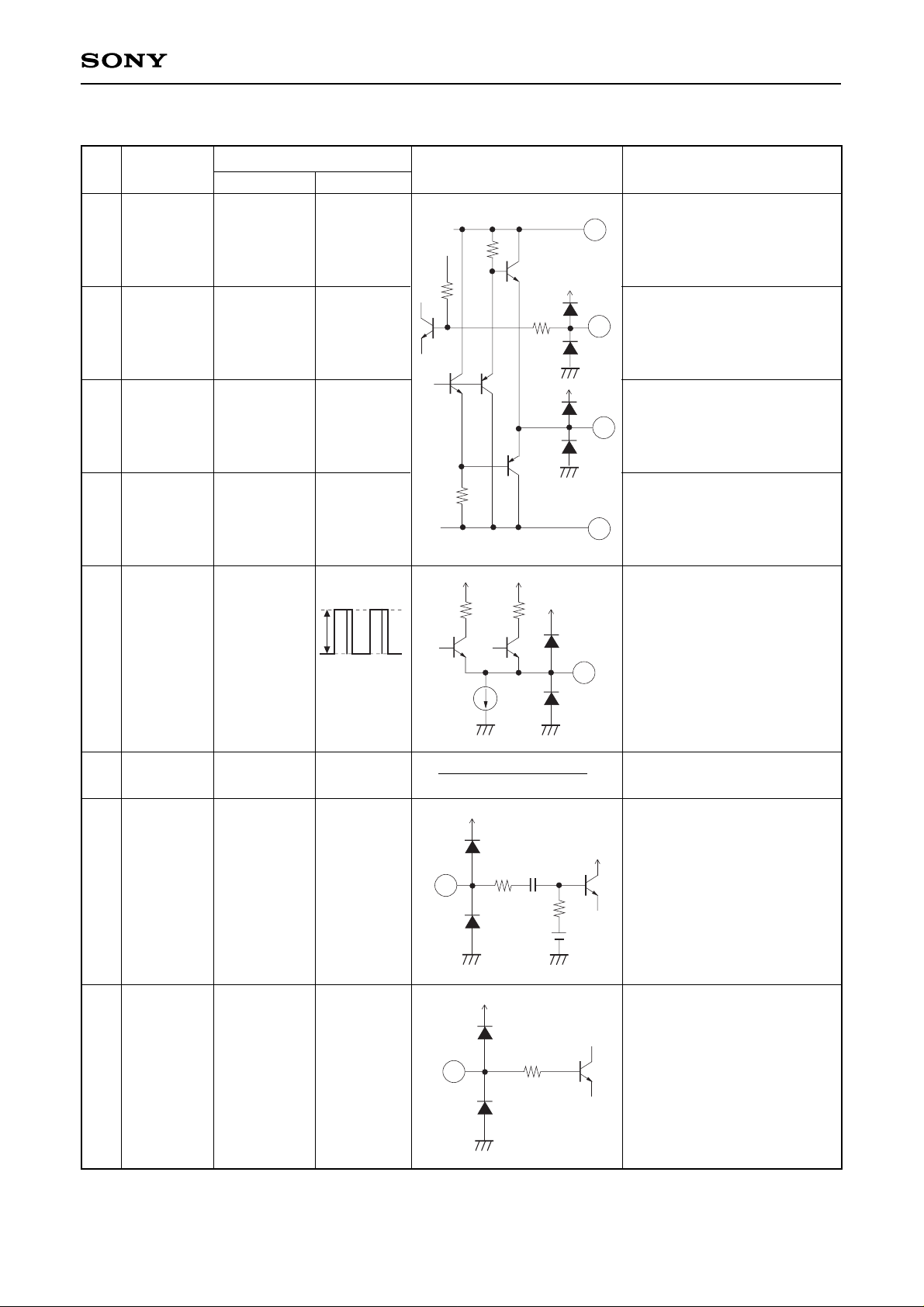
Chroma emphasis f0 (center
frequency) adjustment. (Refer
to item 7 on Description of
Operation.)
Main emphasis and main deemphasis time constant.
When recording, the
emphasized Y signal prior to
white/dark clipping is output.
Main emphasis and main deemphasis time constant.
Apply an external constant
between this pin and Pin 2, as
shown below.
HPF time constant that forms
sub emphasis and sub deemphasis. Add resistance
between this pin and Pin 11.
During recording, Y emphasis
input. During playback, this
signal to the noise canceler is
input. Performs diode
clamping (sync tip clamping),
with the clamp capacitance
attached externally.
25µA
150
1
1mA
150
2
4k
100
3
100
4
100
150
5
1 C EMPH
CONT
2 MAIN
EMPH
OUT
3 MAIN
EMPH
TC
4 SUB
EMPH
TC
5 EMPH IN
Control
range:
1.8V to 3.8V
2.05V (sync
tip level)
2.05V (when
time constant
connected)
2.05V (when
time constant
connected)
2.05V (sync
tip level)
—
250mVp-p
output
—
—
500mVp-p
input
2 3
VG1
11
4
—5—
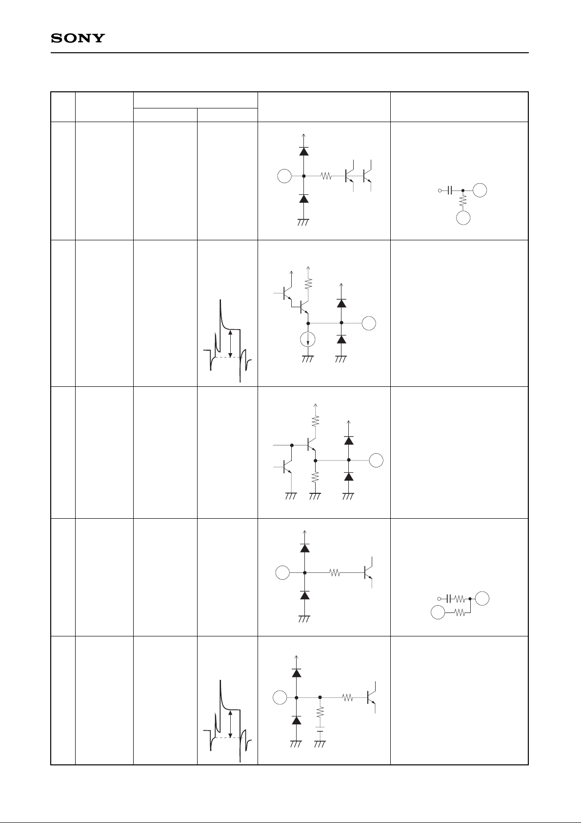
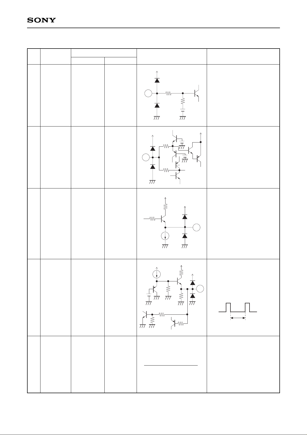
CXA1810AQ/AR
Pin
Symbol
Pin voltage
Equivalent circuit Description
No. DC AC
Connects external time
constant for HPF of noise
canceler. (Refer to item 11 on
Description of Operation.)
Y signal output that has been
FM demodulated and has
passed though the DEMOD
LPF.
During recording, a chroma
signal that has been burst
emphasized, chroma
emphasized, and frequency
converted is output. During
ACK, the output DC goes to
0V. During recording, if
TEST1 is High the burst
emphasized signal is output.
Connects external time
constant for HPF of the
white/dark clipping
compensation circuit during
playback.
Input for de-emphasis circuit
during playback. The signal is
input to the de-emphasis
circuit through the clipping
compensation circuit.
150
6
1mA
63
7
SAT
200
4k
8
150
9
5k
150
2.05V
10
6 NCTC IN
7 DEMOD
OUT
8 REC C
OUT
9 COMP TC
10 DEEMPH
IN
2.05V (when
time constant
connected)
1.6V
2.0V
2.05V (when
time constant
connected)
2.05 V
(center DC)
—
140mVp-p
output during
standard
playback
Lowfrequency
conversion
chroma
signal
300mVp-p
output
—
180mVp-p
input during
playback
VG1
9
11
Input
VG1
6
11
—6—
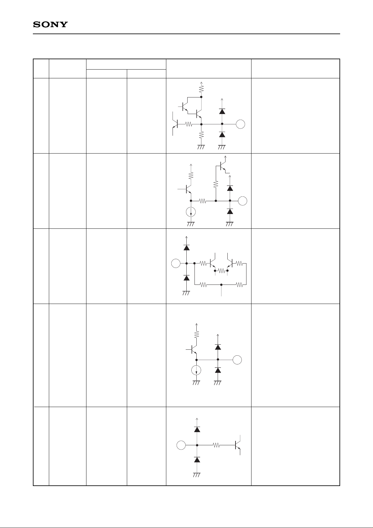
CXA1810AQ/AR
Pin
Symbol
Pin voltage
Equivalent circuit Description
No. DC AC
Internal reference voltage
source. (Can not be used as
external bias for Pins other
than 4, 6, and 9.)
Outputs chroma signal that
has passed through PB C
BPF and chroma feedback
comb filter subtracter
after frequency conversion
during playback.
Connects decoupling
capacitor for limiter of the
playback Y comb block.
Outputs Y signal processed by
comb filter. During playback,
the signal is output through
the sharpness circuit. If mode
E is set High, the signal is
output without passing
through the f sc Trap; if mode
SHP THRU is set High, the
signal is output without
passing through the sharp
-ness circuit.
VCA gain adjustment in the
comb filter block. (Refer to
Adjustment Procedure.)
150
3k
2.5k
11
150
300
0.6mA
270
12
150
150
10k
10k
13
1.4mA
150
14
150
15
11 VG1
12 C TRAP
13 LIM C
14 Y COMB
OUT
15 COMB ADJ
2.05V
2.05V
2.4V
1.2V
(sync tip
level)
Control
range: 1.8V
to Vcc
—
Chroma
signal
300mVp-p
output during
playback
—
Y signal
500mVp-p
output
—
—7—
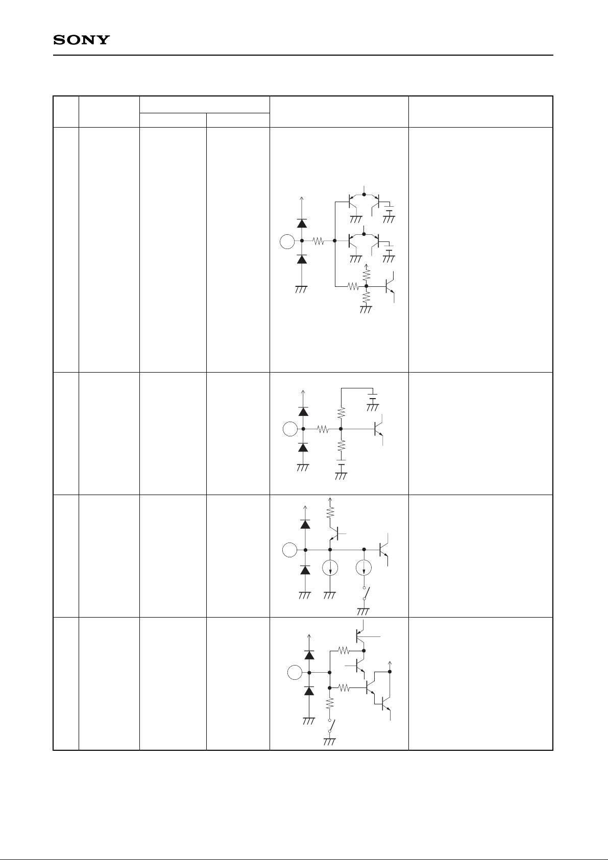
CXA1810AQ/AR
Pin
Symbol
Pin voltage
Equivalent circuit Description
No. DC AC
Time constant for VCA circuit
in comb filter block. A DC
limiter circuit with an upper
limit of 4.0V and a lower limit
of 2.2V is built in.
Connection for inputting the
playback Y signal to the CCD
DL in a system using two CCD
delay lines. When using this
pin, connect 2.2kΩ resistance
to GND.
Time constant for feedback
clamp circuit in the comb filter
block.
Inputs CCD DL (delay line)
output signal to the VCA
circuit.
Time constant for feedback
clamp circuit in the comb filter
block.
150
150
16
150
150
17
150
150
18
40k
150
2.1V
19
150
150
20
16 AGC TC3
17 DL IN2
18 CLAMP
TC3
19 DL OUT2
20 CLAMP
TC2
2.2V to 4.0V
2.2V (when
resistance
connected)
—
2.1V (center
DC)
—
—
Video
500mVp-p
output
—
Video
500mVp-p
input
—
—8—
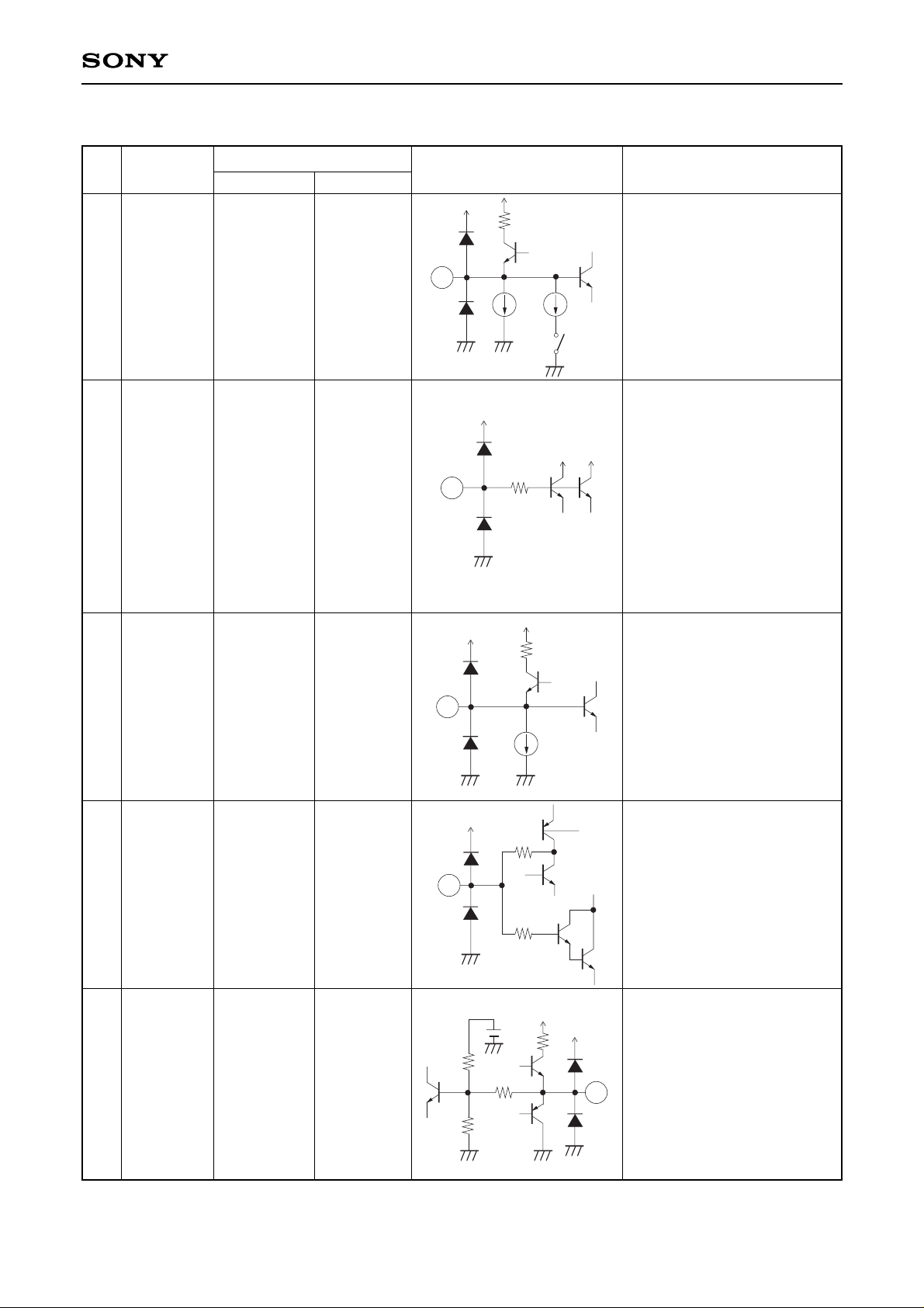
CXA1810AQ/AR
Pin
Symbol
Pin voltage
Equivalent circuit Description
No. DC AC
Inputs CCD DL (delay line)
output signal to VCA circuit.
Time constant for VCA circuit
in the comb filter block. A DC
limiter circuit with an upper
limit of 4.0V and a lower limit
of 2.2V is built in.
Output for inputting a signal to
the CCD DL (delay line).
Normally, Y+C signal is
output. During playback, when
the CCD DL connected to this
pin is used for comb filter
processing of just the C
signal, C signal with quasi
sync is output.
Composite sync signal output.
No output if mode SYNC SEP
OFF is set High.
Main block power supply.
40k
150
2.1V
21
150
150
22
1mA
150
150
23
1H
2.5V
0
270
20k
20k
5k
270
50k
24
21 DL OUT1
22 AGC TC2
23 DL IN1
24 COMP
SYNC
25 VCC
2.1V (center
DC)
2.2V to 4.0V
2.2V
High : 2.5V,
Low : 0V
output
VCC=4.75V
Video
500mVp-p
input
—
Video
500mVp-p
output
—
—
—9—
CXA1810AQ/AR
Pin
Symbol
Pin voltage
Equivalent circuit Description
No. DC AC
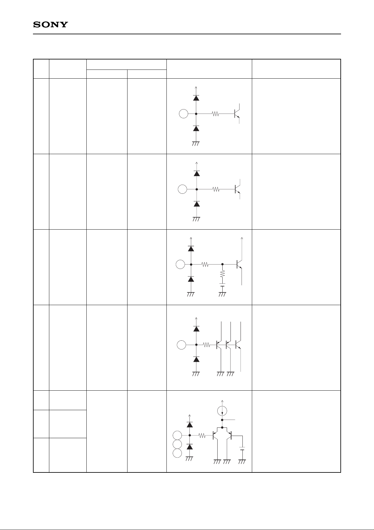
Input for VOW (character
level) signal, VOB (character
background) timing pulse of
DDS (date display system)
and masking timing pulse.
MASK : VTH = 1.1V
DDS : VTH = 2.0V
By varying the input DC for
DDS over a range of 2.3V to
3.0V, the character level can
be changed.
(Refer to item 4 on Description
of Operation.)
Determines the white/dark
clipping levels. During open,
the standard white clipping
level is 235%, and the dark
clipping level is 95%.
(Mode DC1, 2 = Low, High)
(Refer to item 5 on Description
of Operation.)
Video signal input. Performs
diode clamping, with the
clamp capacitance externally
connected. If the mode MUTE
is set High, the charge of the
clamp capacitance is
discharged.
Time constant for the video
AGC circuit in the I/O block.
During mute and playback, the
charge of the external
capacitance is discharged.
150
45k
15k
2.0V
1.1V
16k
26
150
2.05V
10k
4.1V
30k
27
270
100nA
4µA
28
MUTE
ON
100
1k
47k
29
MUTE ON
PB ON
26 DDS/MASK
27 WDC
28 V IN2
29 AGC TC1
2.0V
(when open)
(MASK)
1.5V
(DDS)
2.3 to 3.0V
2.6V
(when open)
2.05V
(sync tip
level)
—
—
—
Video
500mVp-p
input
—
—10—
CXA1810AQ/AR
Pin
Symbol
Pin voltage
Equivalent circuit Description
No. DC AC
Video signal input. Performs
diode clamping, with the
clamp capacitance externally
connected. If the mode MUTE
is set High, the charge of the
clamp capacitance is
discharged.
Level adjustment during
recording. The adjustment
range is 1.3V to 2.6V. During
playback, serves as input for
JOG (variable speed
playback) VD pulse and HD
pulse.
VTH = 2.7V
(Refer to item 3 on Description
of Operation.)
Video signal input for video
out circuit. Performs diode
clamping, with the clamp
capacitance externally
connected.
Time constant for feedback
clamp circuit in I/O block.
I/O block signal output.
270
100nA
4µA
30
MUTE
ON
150
31
270
100nA
32
100
100
33
3k
150
3.4k
27k
2.05V
34
30 V IN1
31 REC L/JVD
32 Y IN
33 CLAMP TC1
34 Y OUT
2.05V
(sync tip
level)
1.9V
(Typical value
during REC
LEVEL
adjustment)
1.6V
(sync tip
level)
—
1.8V
(sync tip
level)
Video
500mVp-p
input
—
Video
500mVp-p
input
—
Video
500mVp-p
output
—11—
CXA1810AQ/AR
Pin
Symbol
Pin voltage
Equivalent circuit Description
No. DC AC
GND for the video out circuit.
Video out 75Ω driver output.
Inverted input for V sag
compensation for the video
out 75Ω driver.
Video out circuit and RF
system block power supply.
During recording, FMmodulated Y signal output.
If mode TEST2 is set High
during recording, the Y signal
after white/dark clipping is
output.
RF system block GND.
During playback, inputs Y-RF
signal to FM modulation
circuit.
During recording, high
luminance smear
compensation, is performed.
This pin also controls the
signal level for FM modulation
circuit.
100
38
37
36
35
2.5mA
6363
39
45k
150
10p
41
150
42
35 VOUT GND
36 VIDEO
OUT
37 INV IN
38 RF/V VCC
39 Y RF OUT
40 RF GND
41 Y RF IN
42 SMEAR
CONT
0V
1.6V
(sync tip
level)
1.5V
VCC=4.75V
2.1V
0V
—
Control
range:
1.8V to Vcc
—
Video
2.0Vp-p
output
Video
1.0Vp-p
input
—
Y FM output
500mVp-p
—
YFM
200mVp-p
input
—
—12—
CXA1810AQ/AR
Pin
Symbol
Pin voltage
Equivalent circuit Description
No. DC AC
During recording, adjustment
for deviation of Y-FM
modulation.
During recording, adjustment
for carrier of Y-FM modulation.
During playback, chroma RF
signal input.
PB C LPF is built in, so that a
signal with the AFM and ATF
components (Y RF + C RF)
eliminated can be input.
RF SWP (switching pulse) and
HCHG (head change) pulse
input. Half H shift, HHS
cancel, ACC channel hold,
and PI/PS switching operate
at VTH = 0.7V. Yd playback
during playback operates at
VTH = 2.05V (same as when
mode Yd is High).
Input to BUS DECODER. CS
is used as chip select, and
data is latched at rising edge.
CK is the clock input. Use a
clock frequency fck of less
than 1.3MHz. SI is used as a
serial input and serial data is
input.
15043150
44
50k
150
3.1V
45
150
46
150
2.05V
47
48
49
43 DEV CONT
44 CARR
CONT
45 PB C IN
46 SWP
47 CS
48 SI
49 CK
Control
range:
1.8V to Vcc
Control
range:
1.8V to Vcc
3.1V
(during
playback)
—
High : Vcc,
Low : 0V
input
—
—
(PB Y RF)
+
(PB C RF
100mVp-p)
input
—
—
—13—
CXA1810AQ/AR
Pin
Symbol
Pin voltage
Equivalent circuit Description
No. DC AC
Drop out pulse input.
VTH = 2.05V
If the drop out pulse is input,
the signal prior to 1H is output
for the Y system and the APC
and ACC system errors are
held for the C system.
Connects an APC external
filter.
Connects an AFC external
filter.
During recording, the chroma
signal is input. When the
typical level is 75% color bar
input, the input signal is
314mVp-p.
Connects a DC feedback
external filter for a nonadjustment VCO.
150
2.05V
100k
50
51
200
PB ON
52
200
200
50k
150
2.6V
53
200 200
200
54
50 D.O.PULSE
51 APC FL
52 AFC FL
53 EXT C IN
54 DCFB
High : 3.1V,
Low : 0V
input
2.25V (typ.)
during lock
2.25V (typ.)
during lock
2.6V
2.25V (typ.)
during lock
—
—
—
(Chroma
signal
314mVp-p
input
—
—14—
CXA1810AQ/AR
Pin
Symbol
Pin voltage
Equivalent circuit Description
No. DC AC
External reference current
source. Connect external
resistance of 18kΩ to GND.
Be careful concerning pin
cross talk.
Main block GND.
Crystal oscillation reference
input. Be careful concerning
pin cross talk and the floating
capacitance.
4.1V regulator output.
Crystal oscillation reference
output. Connects the crystal
between this pin and Pin 57.
Subcarrier input during
camera recording.
200mVp-p(min). Sharpness
control during playback.
20k
55
4k
2V
270
270
2V
57
PB ON
58
100
15k
310
540µA
59
200
60k
9p
60
55 I REF
56 GND
57 XTAL IN
58 VREG
59 XTAL OUT
60 CAM FSC
SHP
1.8V (when
resistance
connected)
0V
2.0V
4.1V
3.1V
Sharpness
control range:
1.8V to VCC
—
—
260mVp-p
(NTSC)
during
playback
—
340mVp-p
(NTSC)
during
playback
—
—15—
CXA1810AQ/AR
Pin
Symbol
Pin voltage
Equivalent circuit Description
No. DC AC
Subcarrier output. This
subcarrier is used for the CCD
delay line clock frequency.
Burst flag and VCO OUT
output for testing. When using
this pin, connect 3.3kΩ
resistance to GND. Serves as
VCO output when mode
TEST2 is High.
During recording, outputs
chroma signal after Y/C
separation or for chroma
signal input from Pin 53.
During playback, the playback
chroma signal is output.
During ACK, the output DC
becomes 0V.
Inputs chroma signal to Y/C
MIX circuit in the I/O block.
During component signal
recording or playback, this
signal is Y/C mixed and is
then output from V OUT.
0.5mA
200
61
20046k
9p
54k
SAT
62
200
2k
100k
63
28k
2.05V
64
61 FSC OUT
62 BF VCO
63 C OUT
64 C IN
2.2V
During BF
output
High : 1.8V,
Low : 0V
Low during
BF interval
2.0V
2.05V
NTSC
600mVp-p
PAL
450mVp-p
550mVp-p
during VCO
output
Chroma
signal
314mVp-p
output
(during
recording)
Chroma
signal
314mVp-p
input
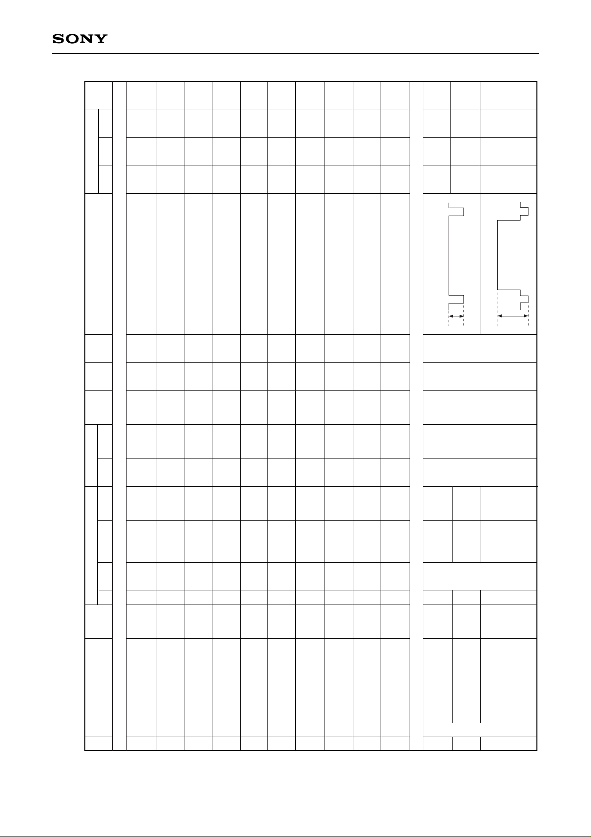
Input conditions Control DC Ratings
—16—
CXA1810AQ/AR
No.
1
2
3
4
5
6
7
8
9
10
11
12
13
Measurement item
Composite signal input
Current consumption
during recording
Separate signal input
Current consumption
during recording
Composite signal input
Current consumption in
power saving mode
Separate signal input
Current consumption in
power saving mode
Current consumption
during playback
Internal reference voltage
source 1
Internal reference
voltage source 1
(V
CC–)
Internal reference
voltage source 1
(V
CC+)
Internal reference
voltage source 2
Reference current
source
SYNC AGC
input Low level
SYNC AGC
input High level
PEAK AGC
Symbol
I
REC1
IREC2
IPS1
IPS2
IPB
VREG
VREG–
VREG+
VG1
IREF
VAGCL
VAGCH
VAGCP
—
—
—
—
—
—
—
—
—
—
e
f
g
—
—
—
—
—
—
—
—
—
—
SG30
Amplitude
—
—
—
—
—
—
—
—
—
—
—
—
—
Frequency
—
—
—
—
—
—
—
—
—
—
—
—
—
—
—
—
—
—
—
—
—
—
—
—
Voltage
—
—
—
—
—
—
—
—
—
—
—
—
—
—
—
—
—
—
—
—
—
SW30
A
C
D
E
F
A
A
A
A
A
B
I
1
I1
I1
I1
I1
P58
P58
P58
P11
P55
P34
Measurement method
V
CC=4.75V, voltage at Pin 58 :VREG
VCC=4.5V, voltage at Pin 58 :VREG1
VREG–=VREG1–VREG
VCC=5.25V, voltage at Pin 58 :VREG2
VREG+=VREG2–VREG
Voltage at Pin 11
IREF=(voltage at Pin 55 )/18k
Measures the output SYNC level.
Measures the output amplitude level.
Min.
63
55
20
35
68
3.90
–12
1.95
94
Typ.
88
78
30
53
94
4.13
–1
+1
2.08
100
143
143
550
Max.
113
100
40
70
120
4.36
+12
2.21
106
Unit
mA
mA
mA
mA
mA
V
mV
mV
V
µA
mV
mV
mV
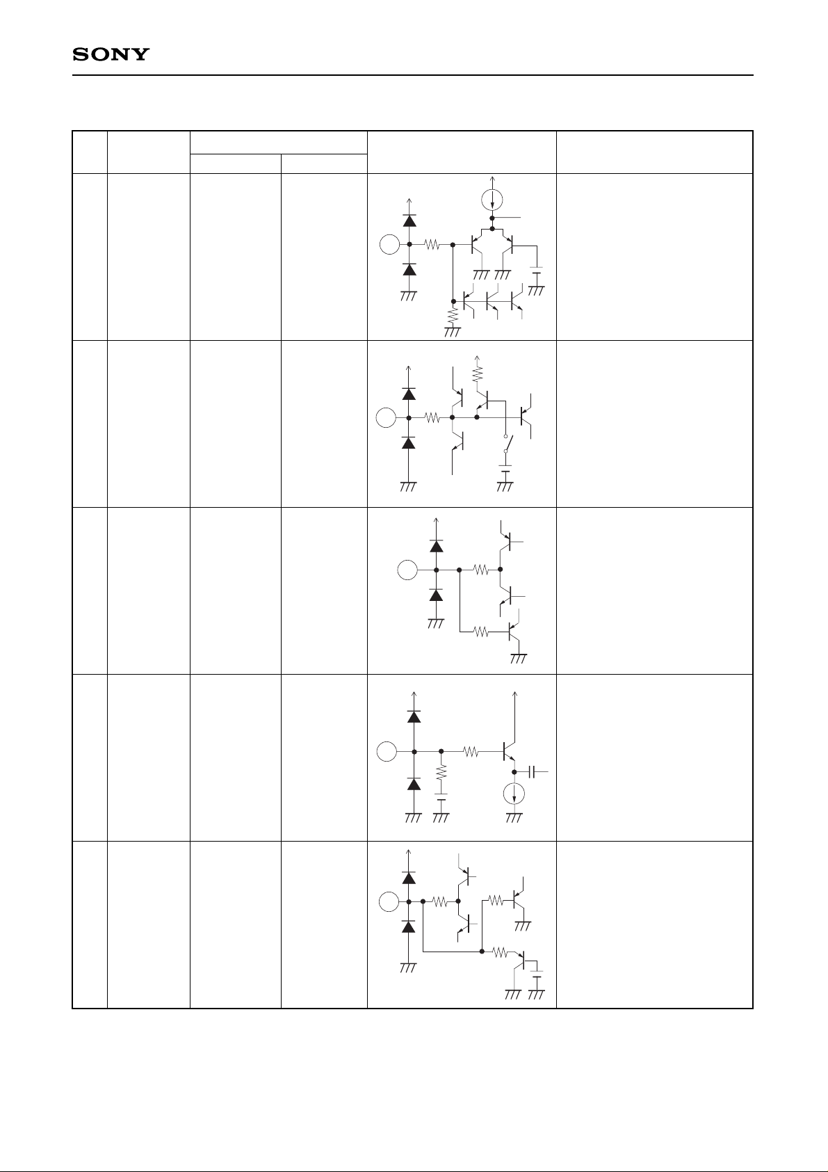
Electrical Characteristics VCC = 4.75V, Ta = 25°C, see Electrical Characteristics Measurement Circuit and BUS DECODER Mode Condition Table.
∗ Start measurements after adjustments in accordance with the Precautions Concerning Measurements.
)
Video AGC
Signal
Signal
source
Voltage
source
SW Mode Measu-
set to condi- rement
ON tions point
<Current consumption, reference bias source>
<Y recording>
(
 Loading...