

Sony CXA1785AR Datasheet

RGB Decoder/Driver
For the availability of this product, please contact the sales office.
Description
The CXA1785AR is an RGB decoder/driver
designed to drive LCD panels. This IC converts
composite video signals, Y/C signals and Y/color
difference signals into RGB signals used for driving
LCDs.
Features
• Both NTSC/PAL compatible
• Supports composite inputs, Y/C inputs and Y/color
difference input
• Band pass filter, trap and delay line
• Sharpness function
• γ compensation circuit
• R, B output delay time adjustment circuit
• Polarity reverse circuit
Applications
• Color liquid crystal viewfinders
• Liquid crystal projectors
• Industrial monitors
Structure
Bipolar silicon monolithic IC
CXA1785AR
48 pin LQFP (Plastic)
Absolute Maximum Ratings (Ta=25°C)
• Supply voltage VCC1-GND 6 V
• Supply voltage VCC2-VEE 15 V
• Supply voltage GND-VEE 10 V
• Input pin voltage VIN VCC1V
•Operating temperature Topr –30 to +85 °C
• Storage temperature Tstg –55 to +150 °C
• Allowable power dissipation
PD 560 mW
Operating Conditions
• Supply voltage VCC1-GND 4.25 to 5.25 V
• Supply voltage VCC2-GND 4.25 to 14.0 V
• Supply voltage VCC2-VEE 11.25 to 14.0 V
• Supply voltage VEE-GND –8.75 to 0 V
Sony reserves the right to change products and specifications without prior notice. This information does not convey any license by
any implication or otherwise under any patents or other right. Application circuits shown, if any, are typical examples illustrating the
operation of the devices. Sony cannot assume responsibility for any problems arising out of the use of these circuits.
—1—
E93Z28-TE
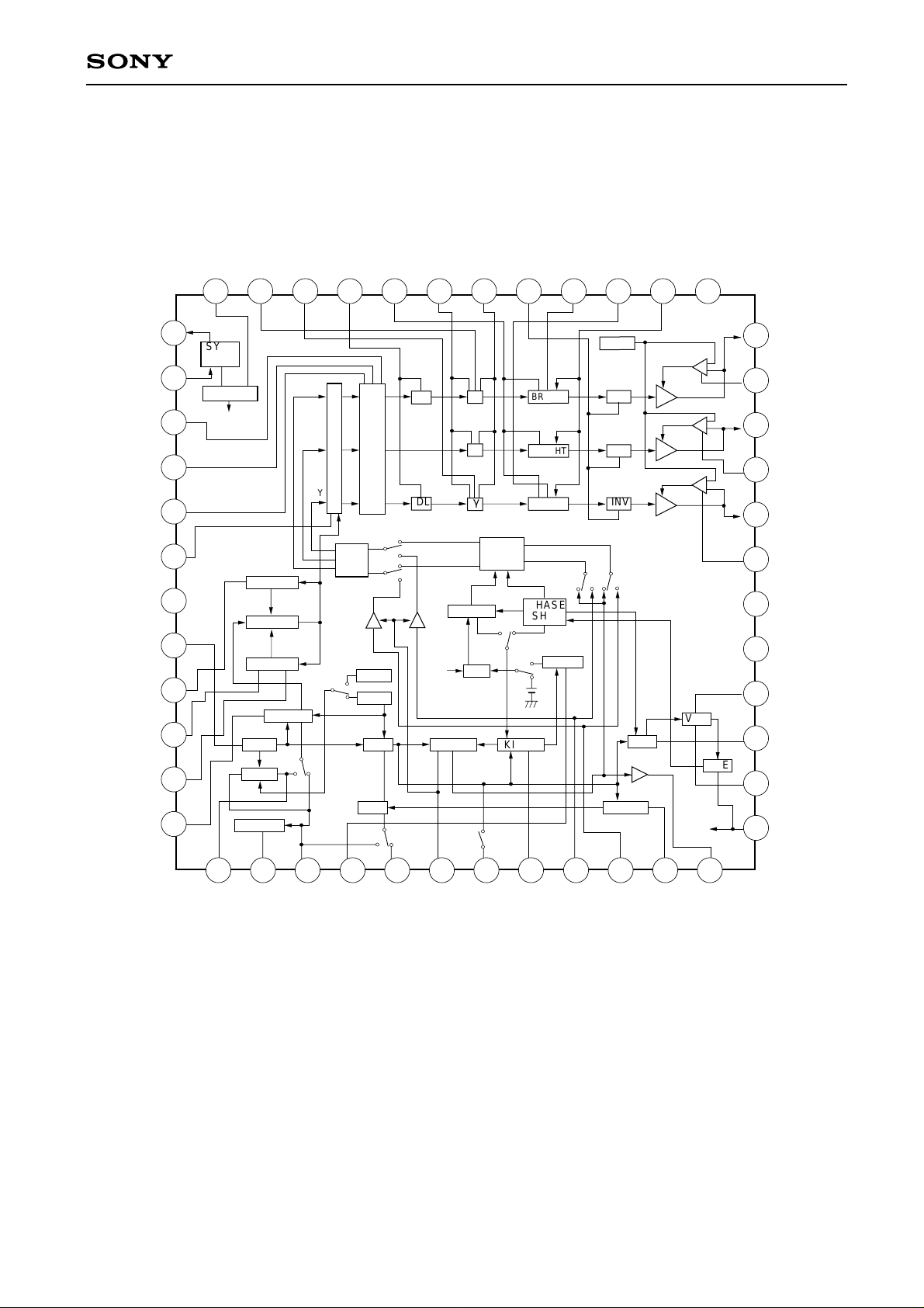
Block Diagram
CXA1785AR
SYNC O UT
SYNC SEP
EXT B IN
EXT G IN
EXT R IN
CONTRAST
F ADJ
CL AMP
AGC FILTER
AGC OUT
PICTURE
37
38
39
40
41
42
43
44
45
46
47
48
SYNC
SEP
BGP GEN
Vcc1
SYNC I N
BGP
SUB
CLAMP
AGC AMP
AGC DET
PI CT URE
REG1
COM P
TRA P
H. F ILTE R
CONTRAST R
SUB
CONTRAST B
DL ADJ
BRIGHT
GAMMA 1
GAMMA 2
FRP
SUB
BRIGHT R
SUB
BRIGHT B
CLIP
252627282930313233343536
2
CC
V
24
B OUT
23
B DC DET
22
G OUT
21
G DC DET
20
R OUT
19
R DC DET
18
17
16
VXO OUT
15
APC FILTER
14
VXO IN
HUE
13
G-Y
R-Y
Y/C
B-Y
MATRI
G
GEN
P
N
X
Y
COMP
INT / EXT SW
REG3
REG2
HPF
Y/C
DL
EXT
SYNC
COLOR
PAL SW
PAL ON
γ
γ
γ INVDL
DEMOD
F/F
P
KILLER
N
BRIGHT
BRIGHT
BRIGHT
PHASE
SHIFT
P
IDENT
N
VREF
INV
INV
N
N
P
P
V
EE
GND
VXO
APC
HUE
ACC DETACC
NT/PAL/
COLO R
DEFFER
1 2 3 4 5 6 7 8 9 10 11 12
B-Y
TRAP
OUT
H FILTER
IDENT
VIDEO IN
C IN
FILTER
KILLER
COLO R
BURST OUT
R-Y
FIL TER
ACC F IL T ER
—2—
OUT
CHROMA
CXA1785AR
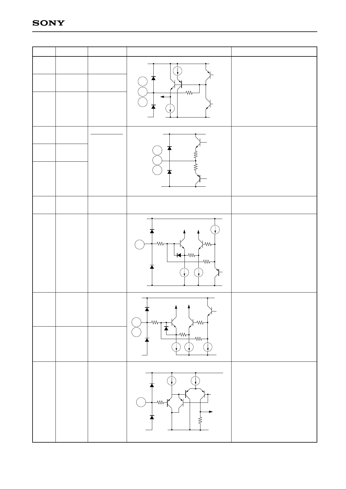
Pin Description (The pin voltage is VCC1 = 4.5 V)
Pin No. Symbol Pin voltage Equivalent circuit Description
1 TRAP 2.0V
CC1
V
Trap connection.
Leave this pin open other than
when composite video input is
1
selected.
2 H FILTER
OUT
3 VIDEO IN 2.25V
4 IDENT
FILTER
VCC1
3
VEE
V
EE
V
CC1
V
VCC1
4
EE
GND
Outputs the video signal to be
input to the sync separation
circuit.
2
GND
Composite video signal input
(Y signal when using Y/C input
and Y/color difference input).
The standard input level is 0.5
VP-P (from sync tip to 100 %
white).
GND
IDENT detection filter connection.
Leave this pin open other than
when PAL mode is selected.
5 C IN 2.5V
V
CC1
V
5
EE
VEE
—3—
GND
Chroma signal input when
using Y/C input. Composite
video signal input is supported
when this pin is connected to
GND. Leave this pin open
when Y/color difference input.
The standard input level is
GND
0.15 VP-P (burst).
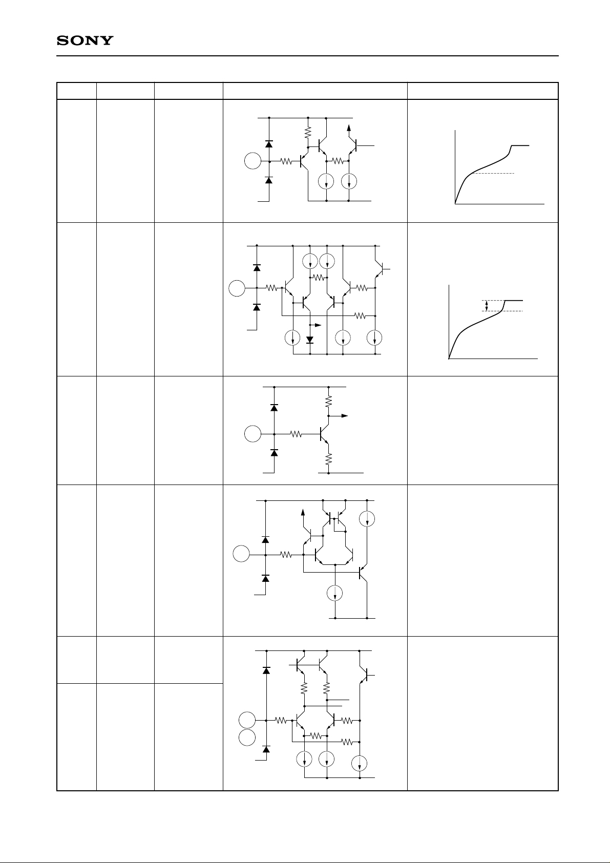
Pin No. Symbol Pin voltage Equivalent circuit Description
6 COLOR
V
CC1
Color adjustment. The amplitude of color difference signal
is adjusted when Y/color
difference input.
6
EE
V
GND
CXA1785AR
7 BURST 3.2V
OUT
8 KILLER
FILTER
9 R–Y 1.9V
10 B–Y 1.9V
V
CC1
9
10
V
VCC1
VEE
V
EE
7
CC1
8
V
EE
GND
GND
GND
Burst cleaning coil is connected for PAL.
Leave this pin open other than
when PAL mode is selected.
Killer detection filter is connected.
Leave this pin open other than
when Y/color difference input
is selected.
Color difference demodulation
circuit inputs. Leave this pin
open for NTSC. Color
difference signal is input when
Y/color difference input.
In this case, input is pedestal
clamped by using external
coupling capacitor.
11 ACC
FILTER
VCC1
11
EE
V
ACC detection filter is connected.
Leave this pin open for Y/color
difference input.
—4—
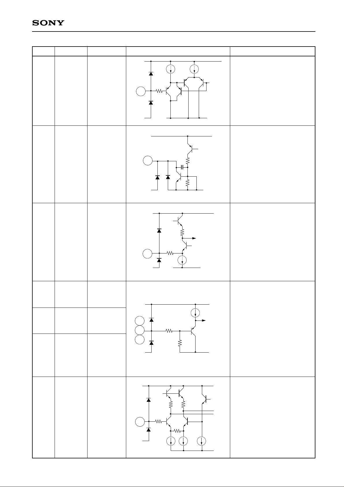
Pin No. Symbol Pin voltage Equivalent circuit Description
12 CHROMA 2.3V
OUT
V
CC1
12
EE
V
GND
Color adjusted and burst taken
out chroma signal is output.
CXA1785AR
13 HUE
14 VXO IN 3.9V
15 APC
FILTER
V
CC1
13
Color phase adjustment pin.
Also doubles as the NTSC,
PAL or Y/color difference
switch. PAL is selected when
this pin is connected to GND;
EE
V
GND
Y/color difference is selected
when this pin is connected to
Vcc1.
VXO input.
CC1
V
Leave this pin open for Y/color
difference input.
14
V
EE
GND
APC detection filter connection.
V
CC1
Leave this pin open for Y/color
difference input.
16 VXO OUT 2.7V
17 GND
18 VEE
V
15
V
EE
16
V
CC1
EE
GND
VXO output.
Leave this pin open for Y/color
difference input.
GND
Ground.
Minimum electric potential connection.
—5—
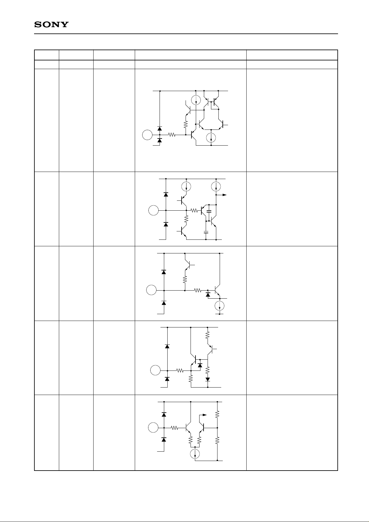
Pin No. Symbol Pin voltage Equivalent circuit Description
19 R DC DET
V
CC1
Smoothing capacitor connection for the feedback circuit
21 G DC DET
23 B DC DET
19
21
23
of RGB output DC level control
. Use a low-leakage capacitor
because this pin has high
impedance.
CXA1785AR
20 R OUT Vcc2+VEE
2
22 G OUT
24 B OUT
25 VCC2
26 CLIP 2.3V
V
VCC1
26
EE
VCC2
20
22
24
VEE
GND
RGB primary color signal
output.
Power supply connection for
RGB output.
Sets the RGB output amplitude (black-black) clip level.
This pin is preset internally.
27 SUB 2.2V
BRIGHT
R
28 SUB 2.2V
BRIGHT
B
29 FRP
GND
VCC1
27
28
VEE
VCC1
29
VEE
Fine adjustment for R and B
signal brightness. Functions
with the γ compensation curve.
This pin is preset internally.
GND
Polarity reverse timing pulse
input for RGB output.
Reversed when low; nonreversed when high.
GND
—6—
Pin No. Symbol Pin voltage Equivalent circuit Description
30 GAMMA1
CC1
V
30
Adjusts voltage gain change
point γ1.
Output
CXA1785AR
γ 1
31 GAMMA2 2.25V
32 BRIGHT
33 DL ADJ 1.2V
34 SUB 2.25V
CONTRAST
R
35 SUB 2.25V
CONTRAST
B
V
CC
31
V
V
V
1
EE
V
VCC1
33
VEE
CC1
34
35
EE
CC1
32
V
EE
GND
GND
GND
Adjusts voltage gain change
point γ2 and the peak limiter
that operates by Vw γ2 above
γ2.This pin is preset internally.
Output
GND
Vwγ 2
RGB output brightness adjustment. Does not function with
the gamma compensation
curve.
Adjusts delay time of R and B
output for G output. The delay
time is adjusted by changing
the resistance value between
this pin and GND. The B
output delay time is twice the R
output delay time.
Connecting this pin to VCC
turns off the R output and B
output delay circuits.
Fine adjustment for R and B
signal contrast. This pin is
preset internally.
Input
Peak limiter
γ 2
Input
V
EE
GND
—7—
Pin No. Symbol Pin voltage Equivalent circuit Description
36 SYNC IN
VCC1
High level input when synchronized; low level at all other
times. The rising edge of the
36
input pulse must precede the
falling edge of the SYNC OUT
pulse. For PAL, the internal flip
flop switches at the rising edge
EE
V
37 SYNC OUT
Vcc1
GND
of the input pulse.
Outputs the sync signal
separated by the sync
separation circuit. High level
37
when synchronized and at low
level in all other cases. This
pin is of an open collector
output. The high level for the
VEE
GND
output should be VEE + 15 V or
less.
38 SYNC SEP 1.8V
VCC1
Sync separation circuit input.
Input the H FILTER output
signal.
CXA1785AR
39 EXT B IN
40 EXT G IN
41 EXT R IN
42 CONTRAST
VCC1
39
40
41
VEE
VCC1
38
VEE
GND
GND
External digital signal input.
There are two threshold
values: VTH1 (approximately
1.2 V) and VTH2 (approximately 2.2 V). When one of
the RGB signals exceeds
VTH1, all of the RGB outputs
go to black level; when an
input exceeds VTH2, only the
corresponding output goes to
white level.
Adjusts RGB output contrast.
42
V
EE
GND
—8—
Pin No. Symbol Pin voltage Equivalent circuit Description
43 VCC1
44 F ADJ 1.2V
Power supply connection.
Connect a resistance between
this pin and GND; the outflow
V
CC1
current value adjusts the
internal filters. Connect 18 kΩ
for both NTSC and PAL.
The following conditions apply
to the resistance connected:
Allowable difference in
resistance: ±2 %
V
44
EE
GND
Temperature characteristics:
±200 ppm
45 CLAMP
CC1
V
Clamps the luminance signal
pedestal level.
Use a low-leakage capacitor
because this pin has high
45
impedance.
CXA1785AR
46 AGC
FILTER
47 AGC OUT
48 PICTURE
V
CC1
V
46
EE
V
VCC1
VCC1
48
47
EE
GND
Connects AGC detection filter
of luminance signal.
GND
Outputs the voltage detected
by the AGC detection circuit of
luminance signal.
When the AGC amplifier gain
is high, the output voltage is
high.
GNDVEE
Adjusts frequency response of
luminance signal. Decreasing
the voltage emphasizes
contours.
V
EE
GND
—9—
 Loading...