

Sony CXA1784AS Datasheet

US Audio Multiplexing Decoder
For the availability of this product, please contact the sales office.
Description
The CXA1784AS is an IC designed as a decoder
for the Zenith TV Multi-channel System and also
corresponds with I2C BUS. Functions include stereo
demodulation, SAP (Separate Audio Program)
demodulation, dbx noise reduction and sound
processor. Various kinds of filters are built in while
adjustment, mode control and sound processor
control are all executed through I2C BUS.
CXA1784AS
42 pin SDIP (Plastic)
Features
• Audio multiplexing decoder, dbx noise reduction
decoder and sound processor are all included in a
single chip. Almost any sort of signal processing is
possible through this IC.
• All adjustments are possible through I2C BUS to
allow for automatic adjustment.
• Various built-in filter circuits greatly reduce external
parts.
• There are two systems for both inputs and outputs,
and each mode control is possible.
Standard I/O Level
• Input level
COMPIN (Pin 17) 245 mVrms
AUXIN-L/R (Pins 38 and 37) 490 mVrms
• Output level
TVOUT-L/R (Pins 35 and 34) 490 mVrms
LSOUT-L/R (Pins 6 and 5) 490 mVrms
Absolute Maximum Ratings (Ta=25°C)
• Supply voltage VCC 11 V
• Operating temperature Topr –20 to +75 °C
• Storage temperature Tstg –65 to +150 °C
• Allowable power dissipation
PD 2.2 W
Range of Operating Supply Voltage
9±0.5 V
Applications
TV, VCR and other decoding systems for US audio
multiplexing TV broadcasting
Structure
Bipolar silicon monolithic IC
Pin Configuration (Top View)
BASSR1
TREL
AUXIN-L
SURRTC
LSOUT-R
SURROUT
BASSR2
BASSL1
1 2 3 4 5 6 7 8 9
TRER
BASSL2
Sony reserves the right to change products and specifications without prior notice. This information does not convey any license by
any implication or otherwise under any patents or other right. Application circuits shown, if any, are typical examples illustrating the
operation of the devices. Sony cannot assume responsibility for any problems arising out of the use of these circuits.
AUXIN-R
LSOUT-L
NC
SDA
TVOUT-L
TVOUT-R
10 11 12 13 14 15 16 17 18 19 20 21
SCL
DGND
ITIME
SAD
VCATC
3233343536373839404142 31
VGR
VCAWGT
IREF
VCAIN
MAININ
VETC
VEOUT
MAINOUT
PLINT
VEWGT
STFIL
VE
COMPIN
– 1 –
SAPIN
SAPTC
SAPOUT
SUBOUT
GND
STIN
NOISETC
222325 242627282930
CC
V
E95430A5Z-PK
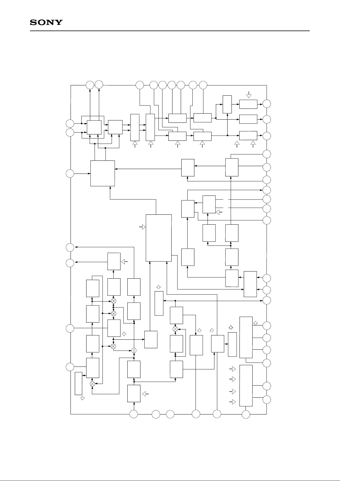
Block Diagram
AUXIN-R
AUXIN-L
CXA1784AS
TVOUT-R
TVOUT-L
34
35
37
38
SW1
SW2
SURRTC
39
PREVOL
BASSL1
42
SURROUND
BASSL2
BASSR1
1
40
BASS
TREL
3
TREBBASS
TREB
TRER
2
MATRIX
SURR-VOL
VOL-S
VOL-R
VOL-L
(L-R)
4
5
6
SURROUT
LSOUT-R
LSOUT-L
BASSR2
41
MAININ
MAINOUT
SUBOUT
PLINT
TREBLEBASSSURRPREVOL
13
MATRIX
SAPC
NRSW/FOMO/
EXT1/EXT2/M1/M2
14
19
1/2
1/4
15
VCO
VCA
WIDEBAND
LPF
FLT
LPF
DeEm
"STEREO"
LOGIC
"SAPVCO"
(+6dB)
SAPVDET
STIND
VCA
VE
DeEm
LPF
SAPVCO
RMSDET
SPECTRAL
HPF
AMP
"SAP"
"NOISE"
DET
NOISE
SAPIND
VOL-LVOL-R
32
VCATC
31
VCAWGT
RMSDET
LPF
LPF
(+4dB)
"SAPLPF"
C BUS I/F
2
I
SAPFDET
SW
"PONRES"
30
29
28
27
26
20
25
24
7
8
9
VCAIN
VEOUT
VETC
VEWGT
VE
STIN
SAPIN
SAPOUT
SDA
SCL
DGND
STFIL
SAD
16
LFLT
STLPF
"STLPF"
LPF
VCA
17
COMPIN
INSW2
INSW1 &
21
CC
V
BPF
23
GND
22
NOISETC
SAPLPF
STLPF
SAPVCO
STVCO
18
SAPTC
IREF
33
ITIME
10
IREF
12
11
VGR
– 2 –
CXA1784AS
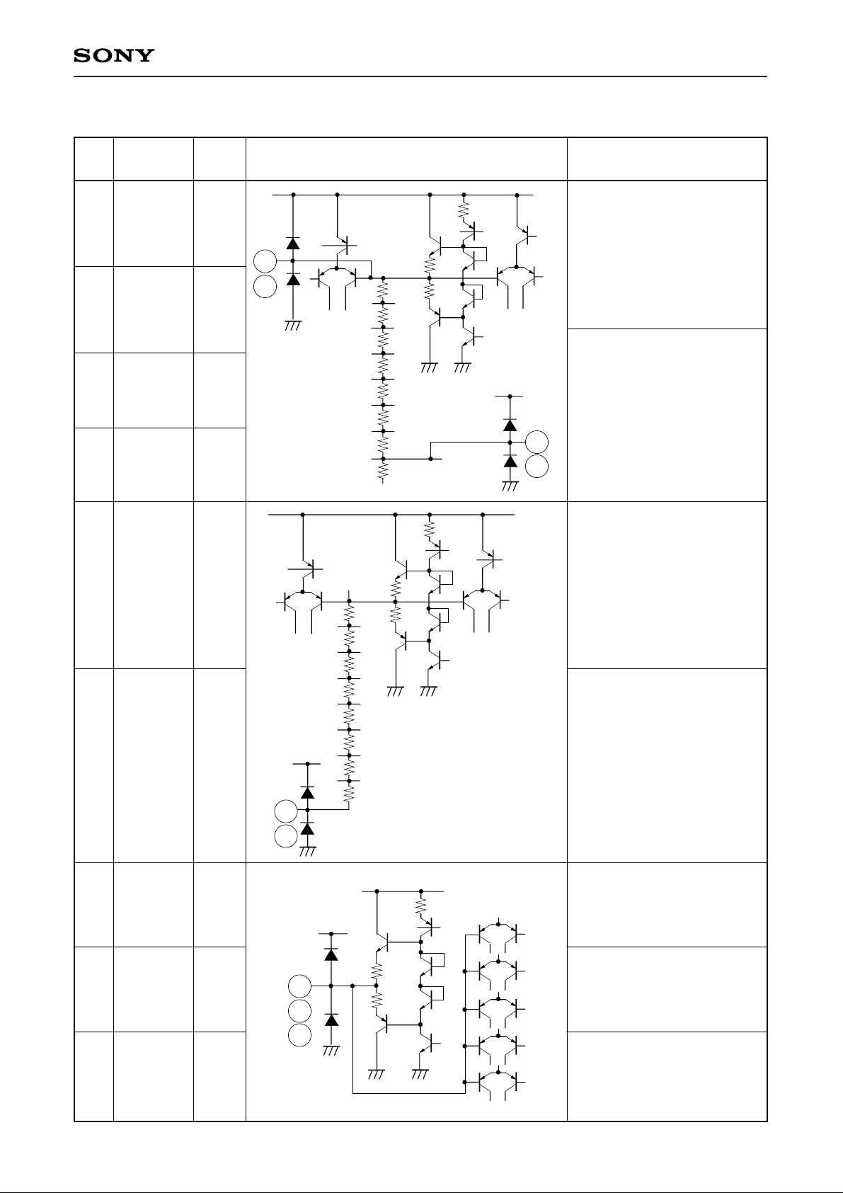
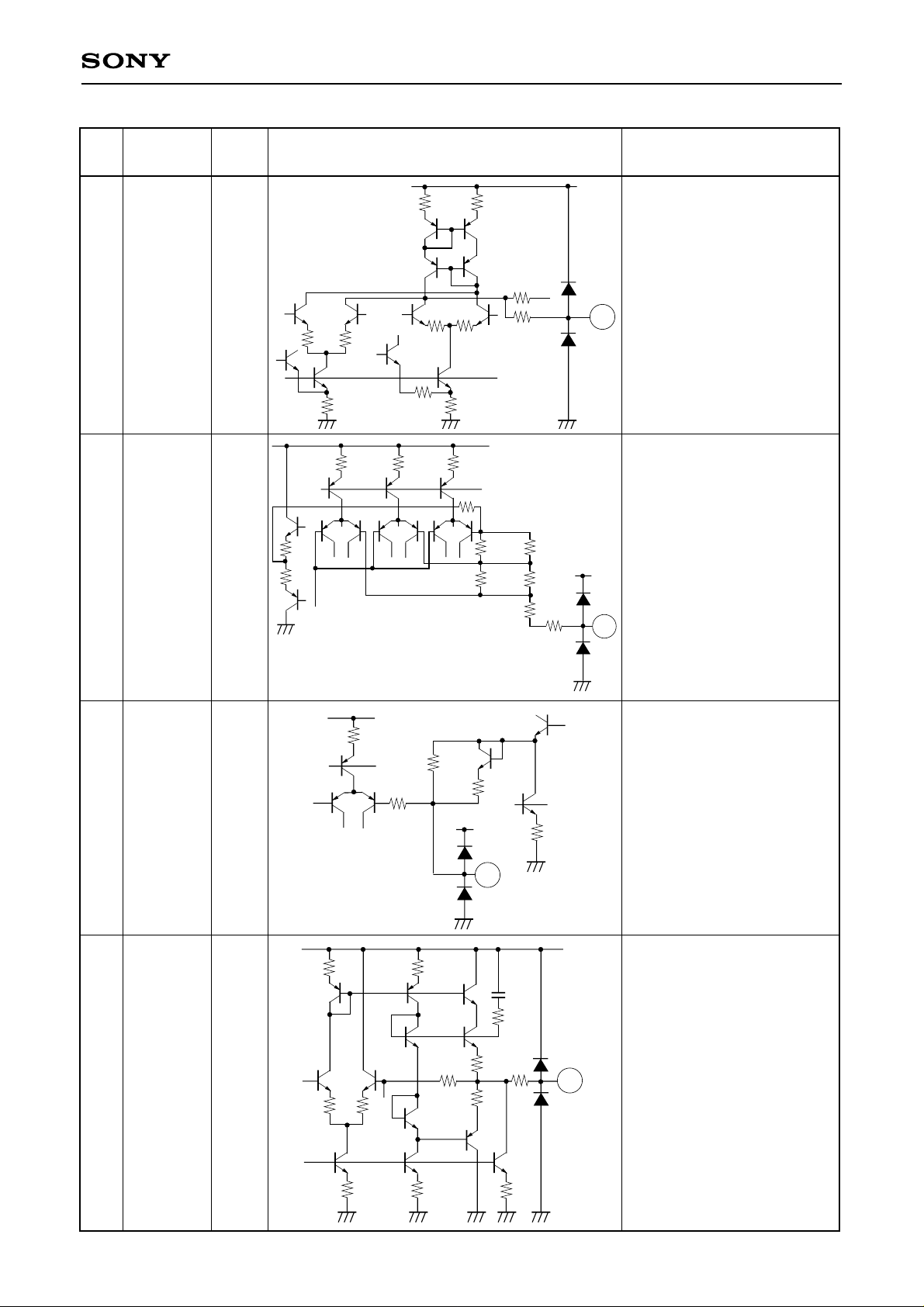
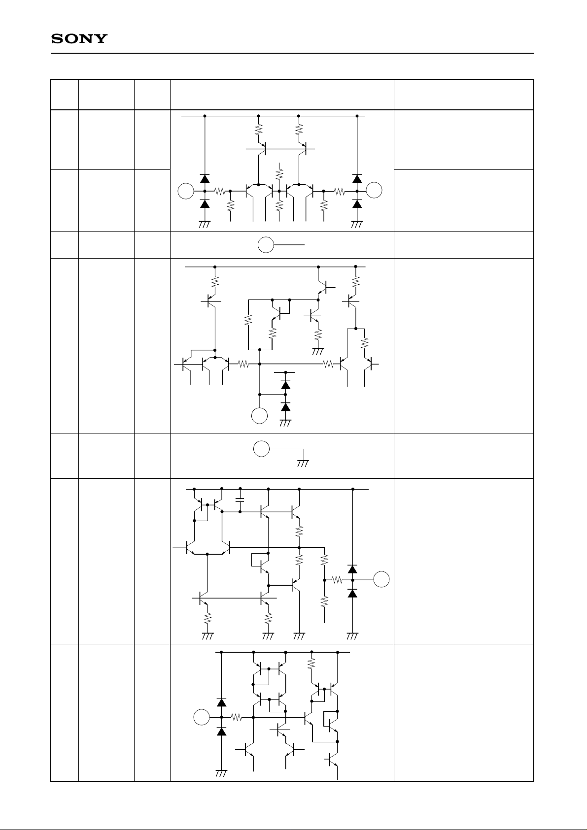
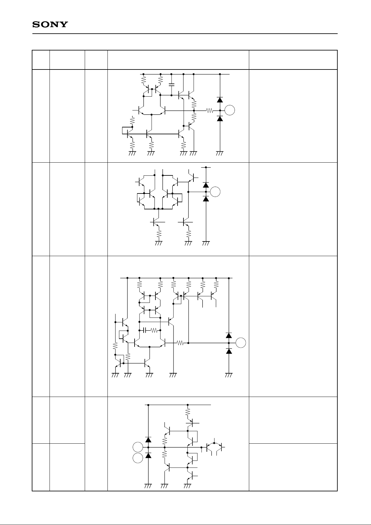
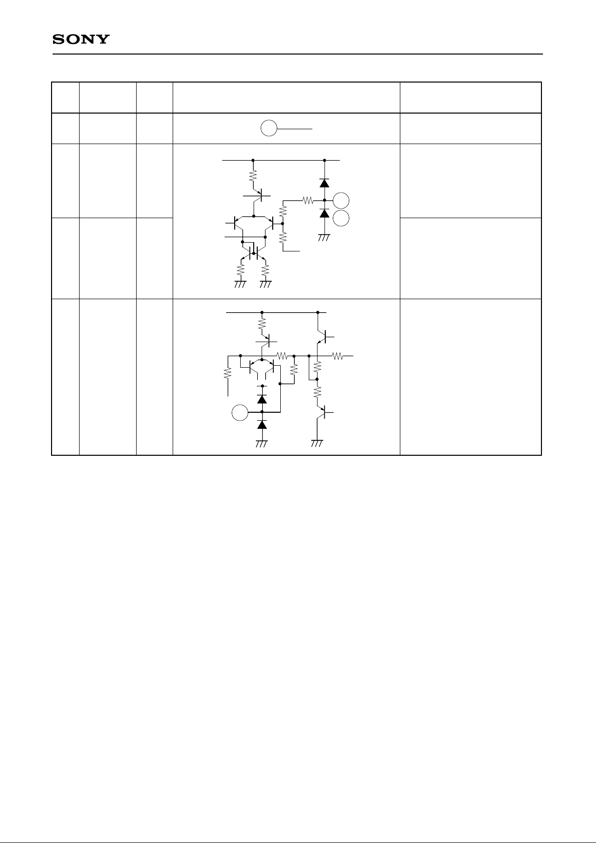
Pin Description (Ta = 25 °C, VCC = 9 V)
Pin
No. voltage
1
42
41
40
2
Symbol
BASSL2
BASSL1
BASSR2
BASSR1
TRER
Pin
4.0
4.0
4.0
4.0
4.0
41
Equivalent circuit Description
BASS filter pin. (Left channel)
VCC
3k
(Connect a 15 nF capacitor
between Pins 1 and 42.)
1
13.2k
10.7k
8.57k
6.89k
5.66k
4.44k
3.67k
15.3k
4V
500
500
V
VCC
3k
The cutoff frequency is
determined by the built-in
resistor and the external
capacitance.
BASS filter pin. (Right
channel) (Connect a 15 nF
capacitor between Pins 41
CC
and 40.)
The cutoff frequency is
40
determined by the built-in
42
resistor and the external
capacitance.
TREBLE filter pin. (Right
channel)
4.2k
3.42k
500
500
(Connect a 6.8 nF capacitor
between this pin and GND.)
3
4
SURROUT
5
6
TREL
LSOUT-R
LSOUT-L
4.0
4.0
4.0
4.0
VCC
2.73k
2.2k
1.8k
1.42k
TREBLE filter pin. (Left
channel)
1.17k
4.88k
2
3
VCC
(Connect a 6.8 nF capacitor
between this pin and GND.)
(L - R) signal output pin.
VCC
500
4
5
6
500
LSOUT right channel output
pin.
LSOUT left channel output
pin.
– 3 –
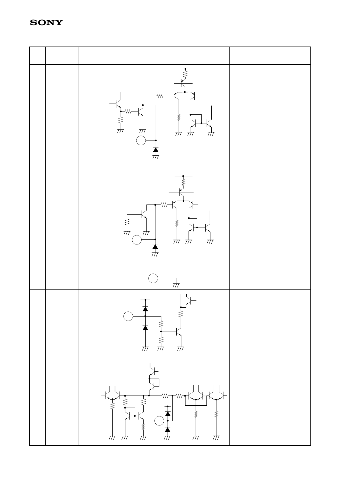
CXA1784AS
Pin
No. voltage
Symbol
7
8
SDA
SCL
Pin
—
—
7.5k
19.5k
× 2
Equivalent circuit Description
V
CC
7.5k
↓ 35µ
2.1V
Serial data I/O pin.
VIH > 3.0 V
VIL < 1.5 V
4.5k
× 5
4k
3k
7
VCC
7.5k
↓ 35µ
4k
2.1V
Serial clock input pin.
VIH > 3.0 V
× 4
3k
VIL < 1.5 V
9
10
11
DGND
SAD
VGR
—
—
1.3V
11k
10
9.7k
8
VCC
19.4k
× 4
2.06k
9
80k
10k
11
3k
VCC
147
40k
2V
11k
Digital block GND.
Slave address control switch.
The slave address is selected
by changing the voltage
applied to this pin.
Band gap reference output
pin. (Connect a 10 µF
capacitor between this pin
and GND.)
11k
– 4 –
CXA1784AS
Pin
No. voltage
12
13
Symbol
IREF
MAININ
Pin
1.3V
4.0V
CC
V
40k 40k 30k
30p 1.8k
6.3k
VCC
13
Equivalent circuit Description
30k 15k 30k
× 2
Set the filter and VCO
reference current. The
reference current is adjusted
VCC
with the BUS DATA based on
the current which flows to this
147
12
pin. (Connect a 62 kΩ (±1%)
resistor between this pin and
GND.)
16k
VCC
23k
23k
↓ 10µ
Input the (L + R) signal from
147
47k
MAINOUT (Pin 14).
14
15
MAINOUT
PLINT
4.0V
6.3V
14
VCC
15k
20k
147
4V
15k
20k
V
CC
× 4
15k
(L + R) signal output pin.
↓
200µ
1k
VCC
Pilot cancel circuit loop filter
147
15
integrating pin.
(Connect a 1 µF capacitor
between this pin and GND.)
26µ
20k
↓
50µ
10k
↓
– 5 –
CXA1784AS
Pin
No. voltage
16
17
Symbol
STFIL
COMPIN
Pin
5.3V
4.0V
500
500
Equivalent circuit Description
75k 75k
12k
11k 11k 11k
1k
4k
3k
4k
1k
27.66k
3k
VCC
27.66k
34.86k
150k
147
27.66k
34.86k
VCC
Stereo block PLL loop filter
16
integrating pin.
Audio multiplexing signal
input pin.
VCC
18
SAPTC
4.5V
4V
8k
24.06k
147
V
CC
10k
3k
1k
17
Set the time constant for the
SAP carrier detection circuit.
VCC
4k
↓ 50µ
18
Vcc
2k2k
10P
4k
(Connect a 4.7 µF capacitor
between this pin and GND.)
19
SUBOUT
4.0V
2k 2k
2k 4k 1k
14.4k
– 6 –
500
500
147
19
(L - R) signal output pin.
CXA1784AS
Pin
No. voltage
20
25
21
22
Symbol
STIN
SAPIN
VCC
NOISETC
Pin
4.0V
4.0V
—
3.0V
20
Equivalent circuit Description
V
CC
23k
23k
Input the (L - R) signal from
SUBOUT (Pin 19).
11.7k
147
47k
8k
× 2
4V
10k
3k
20k
21
1k
Vcc
4V
2k
3k
147
47k
Vcc
3.3k
25
4k
Input the (SAP) signal from
SAPOUT (Pin 24).
Supply voltage pin.
Set the time constant for the
noise detection circuit.
(Connect a 4.7 µF capacitor
and a 200 kΩ resistor
4V
between this pin and GND.)
23
24
26
GND
SAPOUT
VE
—
4.0V
4.0V
26
24k
↓ 10µ
147
5P
22
23
4k
↓ 50µ
500
500
4V
7.5k
7.4k
147
17k
Analog block GND.
Vcc
SAP FM detector output pin.
24
V
CC
Variable de-emphasis
integrating pin.
(Connect a 2700 pF
capacitor and a 3.3 kΩ
resistor in series between
this pin and GND.)
– 7 –

CXA1784AS
Pin
No. voltage
27
28
Symbol
VEWGT
VETC
Pin
4.0V
1.7V
27
147
Equivalent circuit Description
Vcc
Weight the variable deemphasis control effective
500
500
2.9V
4V
36k
value detection circuit.
(Connect a 0.047 µF
capacitor and a 3 kΩ resistor
in series between this pin and
GND.)
8k
30k
↓ 8µ
4k
↓ 50µ
Vcc
Determine the restoration
time constant of the variable
de-emphasis control effective
× 4
× 4
28
value detection circuit. (The
specified restoration time
constant can be obtained by
connecting a 3.3 µF capacitor
between this pin and GND.)
4k
↓ 50µ
20k
↓ 7.5µ
29
30
VEOUT
VCAIN
4.0V
4.0V
29
Vcc
VCC
500
500
20k
47k
VCC
30
10k
47k
5P
Variable de-emphasis output
pin.
(Connect a 4.7 µF non-polar
capacitor between Pins 29
and 30.)
VCA input pin.
Input the variable deemphasis output signal from
Pin 29 via a coupling
capacitor.
– 8 –
CXA1784AS
Pin
No. voltage
31
32
Symbol
VCAWGT
VCATC
Pin
4.0V
1.7V
2.9V
↓
50µ
Equivalent circuit Description
40k 40k
3p
VCC
Weight the VCA control
effective value detection
circuit.
(Connect a 1 µF capacitor
36k
500
500
147
31
and a 3.9 kΩ resistor in series
4k
30k 8k
↓
8µ
VCC
between this pin and GND.)
Determine the restoration
time constant of the VCA
× 4
32
× 4
control effective value
detection circuit.
(The specified restoration
time constant can be
obtained by connecting a 10
↓
50µ
4k
↓
7.5µ
20k
µF capacitor between this pin
and GND.)
33
34
35
ITIME
TVOUT-R
TVOUT-L
1.3V
4.0V
2.6V
47k
× 4
40k 40k 30k
30p 1.8k
25k
500
34
500
35
147
20k 40k 10k
VCC
3k
Set the reference current for
the effective value detection
VCC
timing current. The reference
current is adjusted with the
BUS DATA “SPECTRAL”
based on the current which
flows to this pin.
The timing current determines
the restoration time constant
33
of the detection circuit and
the variable de-emphasis
characteristics.
(Connect a 43 kΩ (±1%)
resistor between this pin and
GND.)
TVOUT right channel output
pin.
TVOUT left channel output
pin.
– 9 –
CXA1784AS
Pin
No. voltage
36
37
38
39
Symbol
NC
AUXIN-R
AUXIN-L
SURRTC
Pin
—
4.0V
4.0V
4.0V
Equivalent circuit Description
36
36
VCC
Right channel external input
pin.
Left channel external input
pin.
Set the central frequency of
the SURROUND circuit phase
shifter.
The frequency is determined
by the built-in resistor and the
19.6k
20k
23k
147
27.6k
47k
4V
20k
23k
20k
CC
V
24k
37
38
VCC
40k
500
500
external capacitance.
39
(Connect a 0.022 µF capacitor
between this pin and GND.)
—
– 10 –
CXA1784AS
= 100mVrms
INSW1 = 0
INSW1 = 1
= 200mVrms
INSW2 = 1
= 490mVrms
= 980mVrms
INSW2 = 0
Unit
Max.
(Ta = 25°C, Vcc = 9V)
Typ.
Min.
= 20mVrms
= 60mVrms
= 98mVrms
= 294mVrms
Output pin
Filter
Measurement
mA
53
44
35
conditions
mVrms
540
490
440
34/35
dB
1.0
1.0
0
-1.0
-1.2
-3.0
34/35
34/35
20 log ('5k'/'1k')
20 log
('12k'/'1k')
%
0.5
0.1
—
34/35
15kLPF
0.5
0.15
—
34/35
15kLPF
20 log
dB
mVrms
—
230
69
190
61
150
19
34/35
15kLPF
('100%'/'0%')
dB
1.0
-0.5
-3.0
19
20 log
('12k'/'1k')
%
1.0
0.1
—
19
15kLPF
2.0
0.2
—
19
15kLPF
20 log
dB
dB
—
-22
64
-30
—
56
19
19
fH BPF
15kLPF
('100%'/'0%')
20 log
('out'/'in')
dB
8.0
-3.0
4.0
-6.0
2.0
-9.0
BUS
RETURN
0dB=49mVrms
20 log (‘on
level’/’off level’)
= 245mVrms
= 490mVrms
= 49mVrms
INSW1 = 0, = 1
INSW2 = 0, = 1
Main (L + R) (Pre-Emphasis : OFF)
= 147mVrms
Input signal
Input pin
Mode
Symbol
SUB (L – R) (dbx-TV :OFF)
fH = 15.734kHz
Pilot
SAP Carrier
Item
No signal
Mono 1kHz 100% mod.
Pre-em. on
Mono 5kHz 30% mod.
Pre-em. on
Mono 12kHz 30% mod.
17
17
MONO
MONO
Icc
Vmain
FCdeem
Current consumption
Main output level
Main de-emphasis frequency
characteristic
Main LPF frequency
Pre-em.on
Mono 1kHz 100% mod.
Pre-em. on
Mono 1kHz 200% mod.
Pre-em off
17
17
17
MONO
MONO
MONO
THDm
FCmain
characteristic
THDmmax
Main distortion
Main overload distortion
Mono 1kHz,
Pre-em on
SUB (L-R), 1kHz,
17
17
ST
MONO
Vsub
SNmain
Main S/N
Sub output level
100% mod., NR OFF
SUB (L-R) 12kHz,
30% mod., NR OFF
SUB (L-R) 1kHz,
100% mod., NR OFF
SUB (L-R), 1kHz,
17
17
17
ST
ST
ST
FCsub
THDsub
THDsmax
Sub LPF frequency
characteristic
Sub distortion
Sub overload distortion
) 0dB
H
200% mod., NR OFF
SUB (L-R) 1kHz,
NR OFF
PILOT (f
17
17
ST
ST
SNsub
Sub S/N
THst
PCsub
Sub pilot leak
Stereo ON level
) Level
H
Change
PILOT (f
17
ST
HYst
Stereo ON/OFF hysteresis
Electrical Characteristics
COMPIN input level
(100% modulation level)
No.
1
2
3
4
5
6
7
8
9
10
11
12
13
14
15
– 11 –

CXA1784AS
Unit
230
Max.
190
Typ.
150
Min.
24
Output pin
Filter
conditions
Measurement
mVrms
610
490
370
34/35
dB
2.5
0
-3.0
24
20 log
('10k'/'1k')
%
6.0
2.5
—
24
15kLPF
1.5
0.6
—
34/35
15kLPF
20 log
dB
—
-5.5
55
-7.0
46
-8.5
24
24
15kLPF
('100%'/'0%')
dBm
-54
-6.0
-75
-9.0
—
-12.0
34/35
15kLPF
0dB=147mVrms
6.0
4.0
2.0
BUS
RETURN
20 log(‘on
—
—
35
35
23
23
34/35
34/35
15kLPF
15kLPF
level’/’off level’)
—
35
23
34/35
15kLPF
dB
—
0.5
0
35
23
-0.5
34/35
34/35
15kLPF
0dB=490mVrms
-59
-75
—
34/35
1kBPF
0dB=490mVrms
EXT → INT
0dB=490mVrms
INT → EXT
-70
-70
-75
-80
—
—
34/35
1kBPF
20 log (M1="0"/M1="1")
20 log (M1="0"/M1="1")
Input signal
SAP 1kHz 100% mod.
NR OFF
SAP 1kHz 100% mod.
17
Input pin
Mode
Symbol
SAP
Vsap1
Vsap2
Item
NR ON
SAP 10kHz, 30% mod.
NR OFF
SAP 1kHz 100% mod.
NR OFF
SAP 1kHz 100% mod.
17
SAP
FCsap
17
SAP
THDsap1
NR ON
SAP 1kHz, NR OFF
17
SAP
SNsap
THDsap2
) Level
SAP 1kHz, 100% mod.
NR OFF
No signal
Change
SAP Carrier (5f
17
SAP
Smute
SAP
Ndbx
17
SAP
THsap
H
ST-L 300Hz 30% mod.
NR ON
ST-R 300Hz 30% mod.
17
ST
HYsap
STLsep1
NR ON
ST-L 3kHz 30% mod.
NR ON
ST-R 3kHz 30% mod.
17
17
17
ST
ST
ST
STLsep2
STRsep1
STRsep2
NR ON
Sine wave 1kHz,
490mVrms
Sine wave 1kHz,
37/38
EXT
Vtv
490mVrms
MONO 1kHz, 100%,
Pre-em. on
MONO 1kHz, 100%,
17
37/38
INT
EXT
CTtv1
CTtv2
Pre-em. on
Sine wave 1kHz,
490mVrms
17
37/38
INT
EXT
MUtv1
MUtv2
No.
SAP output level
16
17
SAP LPF frequency
characteristic
SAP distortion
18
19
20
SAP S/N
21
SAP soft mute
dbx out noise level
22
23
SAP ON level
SAP ON/OFF hysteresis
ST separation 1 L → R
24
25
26
– 12 –
ST separation 1 R → L
27
ST separation 2 L → R
28
ST separation 2 R → L
TVOUT output level
29
30
TVOUT
cross talk
31
TVOUT
muted amount
32
33
 Loading...