

Sony CXA1779P Datasheet
– 1 –
CXA1779P
E94510-ST
Predriver for High Resolution Computer Displays
Description
The CXA1779P is a bipolar IC developed for high
resolution computer displays.
Features
• Wide bandwidth (150MHz/–3dB typ.)
• RGB single package
• Permits RGB common and independent contrast
control
• Permits RGB independent pedestal level control
• Input D-range: 0.7Vp-p (min.)
Applications
High resolution computer displays
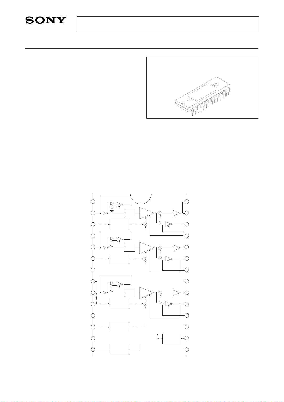
Structure
Bipolar silicon monolithic IC
Block Diagram and Pin Configuration
(Top View)
Absolute Maximum Ratings
• Supply voltage Vcc 14 V
• Operating temperature Topr –20 to +75 °C
• Storage temperature Tstg –65 to +150 °C
• Allowable power dissipation PD 2.8 W
Recommended Operating Conditions
Supply voltage Vcc 12 ± 0.6 V
Sony reserves the right to change products and specifications without prior notice. This information does not convey any license by
any implication or otherwise under any patents or other right. Application circuits shown, if any, are typical examples illustrating the
operation of the devices. Sony cannot assume responsibility for any problems arising out of the use of these circuits.
28 pin DIP (Plastic)
PEDESTAL
CLAMP
1.7V
CLP
SYNC
SLICE
OUTPUT-
BUFFER
BLANKING
ADD
GAIN
+15dB
BLK
BRIGHTNESS
CONTROL
CLP
B CONTRAST
CONTROL
PIX
2
3
4
5
6
7
8
9
10
11
12
13
14
15
16
17
18
19
20
21
22
23
24
25
26
27
28
1
PEDESTAL
CLAMP
1.7V
CLP
SYNC
SLICE
OUTPUT-
BUFFER
BLANK INC
ADD
GAIN
+15dB
BLK
BRIGHTNESS
CONTROL
CLP
R CONTRAST
CONTROL
PEDESTAL
CLAMP
1.7V
CLP
SYNC
SLICE
OUTPUT-
BUFFER
BLANKING
ADD
GAIN
+15dB
BLK
BRIGHTNESS
CONTROL
CLP
G CONTRAST
CONTROL
PIX
PIX
RGB
CONTRAST
CONTROL
PIX
CLAMP
PULSESHAPE
BLANKING
PULSESHAPE
CLP
BLK
Vcc
R IN
R DRV
R GND
G IN
G DRV
G GND
B IN
B DRV
B GND
REG
PIX
GND
CLP
R OUT
R S/H
R BRT
RD GND
G OUT
G S/H
G BRT
GO GND
B OUT
B S/H
B BRT
BO GND
BLK
N.C.
For the availability of this product, please contact the sales office.
– 2 –
CXA1779P
Pin Description
Pin
No.
1
2
5
8
3
6
9
12
4
7
10
11
13
17
21
25
12V
3.0V
—
0V
5V
0V
0V
Vcc
R IN
G IN
B IN
R DRV
G DRV
B DRV
PIX
R GND
G GND
B GND
REG
GND
BO GND
GO GND
RO GND
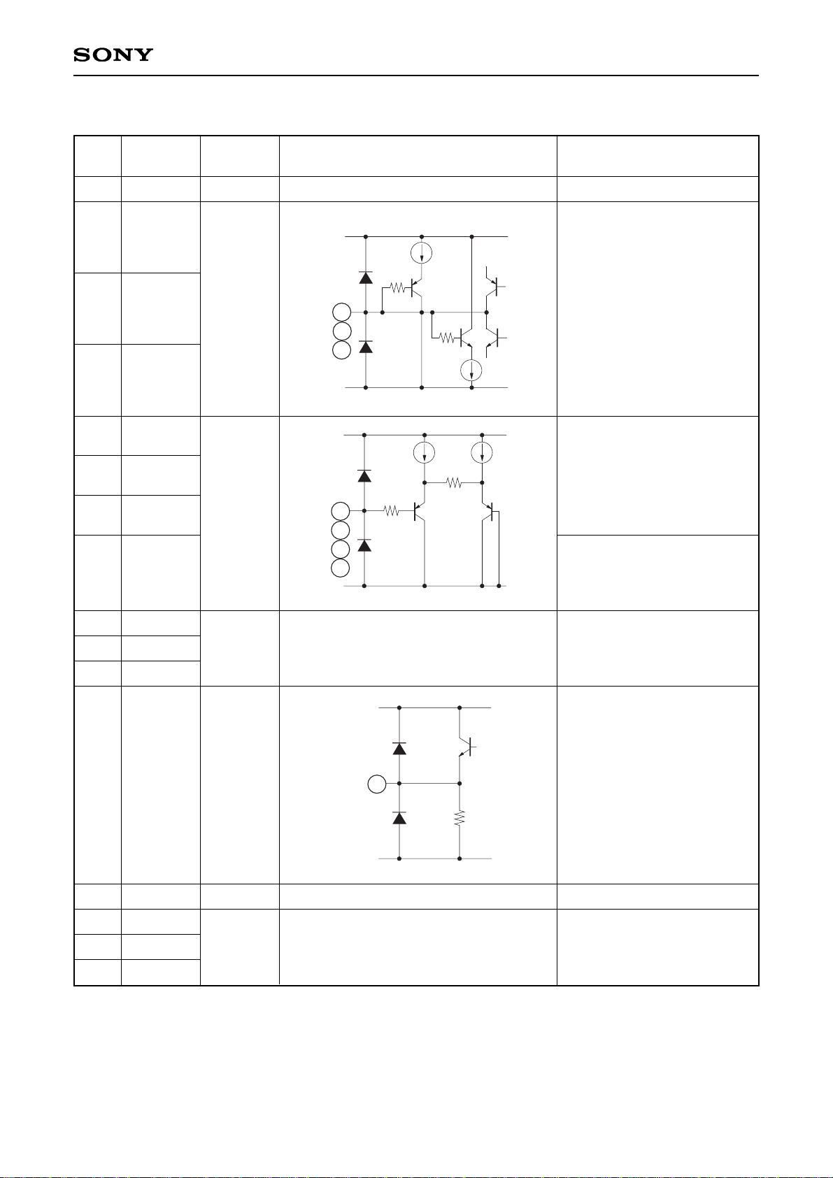
Power supply pin.
RGB input pins.
The pedestal level of the
input signal is 3.0V during
clamping.
Connect 0.01µF in series as
the clamping capacitor.
RGB contrast adjustment
pins.
The variable range of the pin
voltages is from 0 to 5V.
RGB simultaneous contrast
adjustment pin.
The variable range of the pin
voltage is from 0 to 5V.
GND pins for the input
amplifier block.
• Internal regulator stabilizing
pin.
• 5V regulator output pin.
• Attaches the decoupling
capacitance (0.01µF).
GND pin.
GND pins for the output stage
buffer amplifier block.
Symbol Pin voltage Equivalent circuit Description
Vcc
GND
200µA
129
2
5
8
129
200µA
Vcc
200µA
200µA
GND
12
60k
3
6
9
129
Vcc
GND
11
20k
– 3 –
CXA1779P
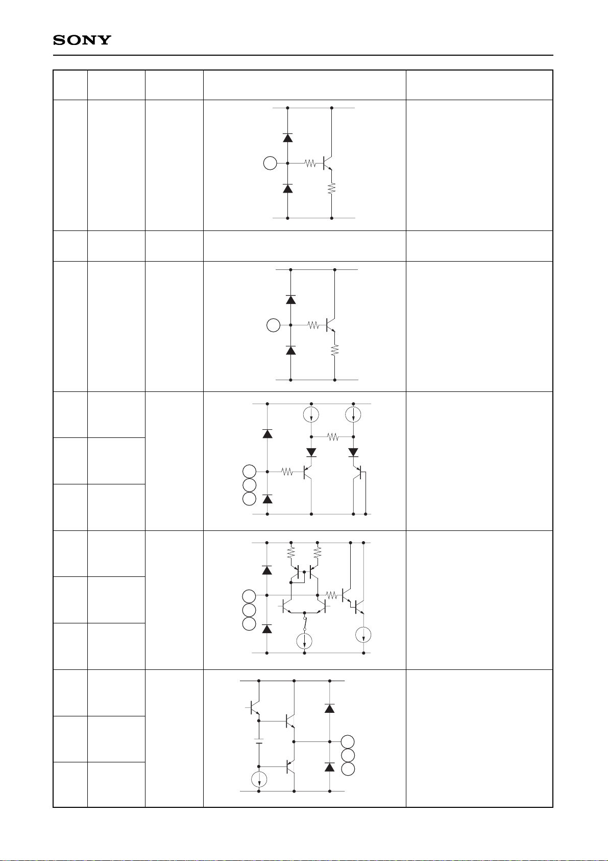
14 —CLP
• Clamp pulse input pin.
• Turns the input clamp and
the bright level adjustment
circuit on and off when high.
VH = 3V
VL = 1.5V
15 —N.C.
Leave this pin open.
Connect to GND.
16 —BLK
• Blanking pulse input pin.
• Threshold level at
approximately 2.25V.
VH = 3V
VL = 1.5V
18—B BRT
22 G BRT
26 R BRT
19 B S/H
23 G S/H
27 R S/H
20 B OUT
24 G OUT
28 R OUT
RGB bright level adjustment
pins.
The variable range of the pin
voltages is from 0 to 5V.
Pins to externally attach the
sample-and-hold capacitor
(0.01µF).
RGB output pins.
Pin
No.
Symbol Pin voltage Equivalent circuit Description
Vcc
GND
Vcc
GND
14
16
129
129
15k
30k
Vcc
GND
Vcc
GND
18
19
23
27
22
26
129
200µA
50k
1k
200µA
Vcc
200µA
100µA
20
24
28
GND
 Loading...