

Sony CXA1746Q Datasheet

Electronic Volume
For the availability of this product, please contact the sales office.
Description
The CXA1746Q is a 2-channel electronic volume
IC. A 34-bit serial data input controls the level and
characteristics of the output signal. It may be used
in car stereos and general audio systems.
Features
• Loudness
• Volume control
(from 0 dB to –87 dB, –∞ dB: Fine (1 dB-step)
Coarse (8 dB-step)
• Balance
• Tone control
(3-band, 2 dB-step from –15 dB to +15 dB)
• Fader
(2 dB-step to –20 dB, –25 dB, –35 dB, –45 dB, –60
dB, –∞ dB)
• Input and gain selector (4 channels)
• Serial data control (DATA, CLK, CE)
• Single 8 V power supply
• Zero-cross detection circuit
• Timer
• Power-off mute
CXA1746Q
48 pin QFP (Plastic)
Absolute Maximum Ratings (Ta=25°C)
• Supply voltage VCC 13 V
• Operating temperature Topr –40 to +85 °C
• Storage temperature Tstg –65 to +150 °C
• Allowable power dissipation
PD 350 mW
(Ta = 85 °C)
Recommended Operating Condition
• Supply voltage VCC 6 to 12 V
Structure
Bipolar IC
Sony reserves the right to change products and specifications without prior notice. This information does not convey any license by
any implication or otherwise under any patents or other right. Application circuits shown, if any, are typical examples illustrating the
operation of the devices. Sony cannot assume responsibility for any problems arising out of the use of these circuits.
—1—
E94812D7Y
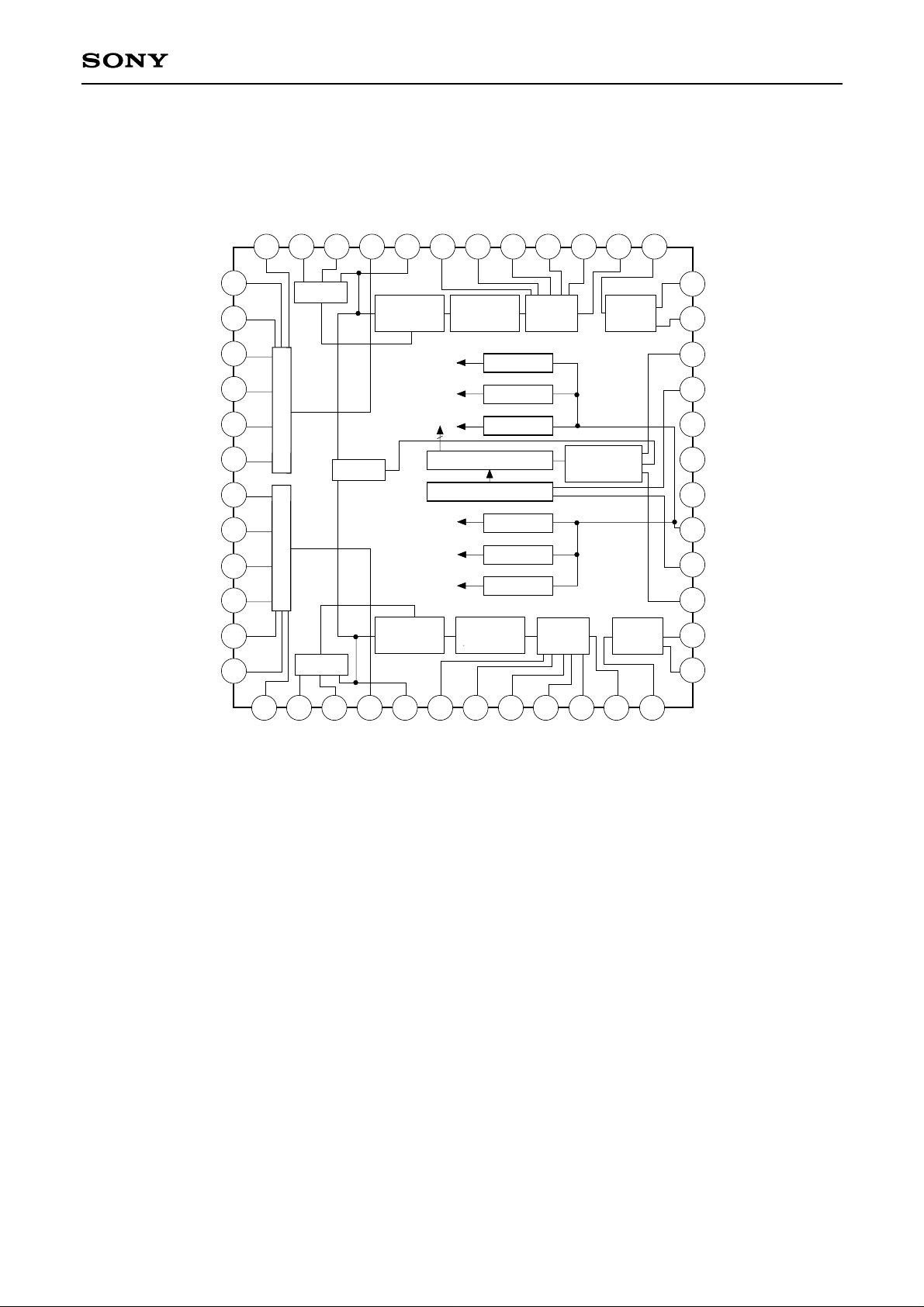
Block Diagram and Pin Configuration
LDHC1
LDLC1
GAIN134
CXA1746Q
FDIN1
TCO1
TCLC12
TCLC11
TCMC12
TCMC11
TCHC1
VRI N1
INAO1
252627282930313233343536
GAIN12
GAIN11
IN14
IN13
IN12
IN11
IN21
IN22
IN23
IN24
GAIN21
GAIN22
37
38
39
40
41
42
43
44
45
46
47
48
INPUT SWITCH
INPUT SWITCH
LOUD
LOUD
ZCDET
8dB STEP
VOLUME
VOLUME
8dB STEP
1dB STEP
VOLUME
LA TCH
SHIFT R EGI STER
VOLUME
1dB STEP
1 2 3 4 5 6 7 8 9
TONE FADER
VCTBUFF
VCTBUFF
VCTBUFF
VCTBUFF
VCTBUFF
VCTBUFF
LA TCH
CONTROL
TONE FADER
10 11 12
24
23
22
21
20
19
18
17
16
15
14
13
FNTO
REO1
CE
CLK
DGND
GND
VCC
VCT
DATA
TIMER
REO
FNTO2
TCO2
LDHC2
INAO2
TCHC2
TCLC22
TCLC21
TCMC22
TCMC21
LDLC2
GAIN234
VRI N2
FDIN2
—2—
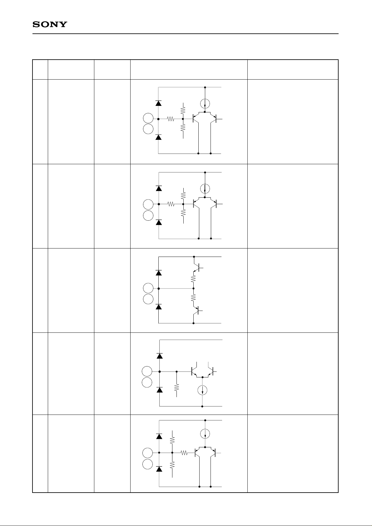
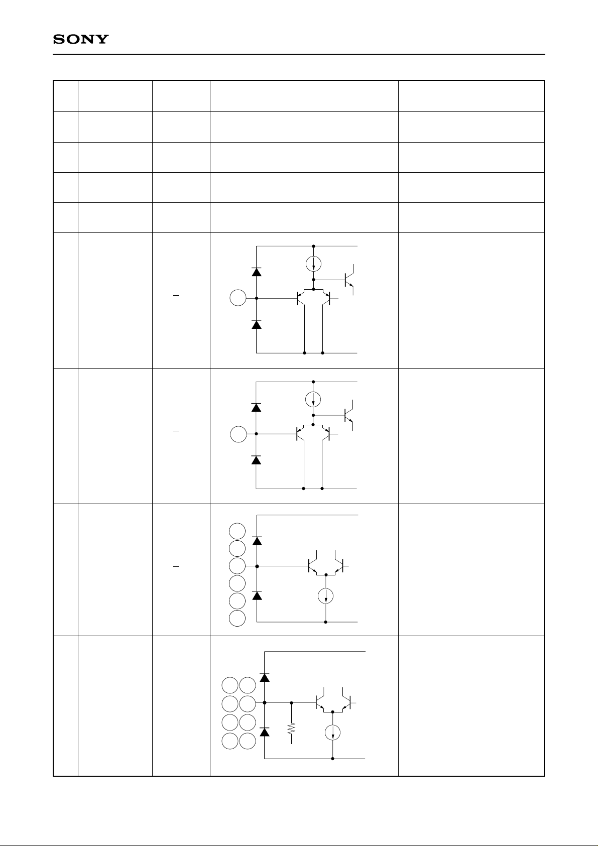
Pin Description and Equivalent Circuit
CXA1746Q
Pin
No. Pin voltage
35
34
2
3
Pin Name
LDLC2
LDLC1
LDHC2
LDHC1
I/O Resistance
6.18k
VCT
8.92k
VCT
Equivalent Circuit Description
VCC
Sets loudness low cut-off
2
35
GND
VCC
frequency.
Set loudness high cut-off
3
34
GND
frequency
4
33
5
32
INAO2
INAO1
VRIN2
VRIN1
—
VCT
10k
VCT
32
33
5
V
CC
4
GND
CC
V
Input selector output
Volume input
GND
V
CC
6
31
TCHC2
TCHC1
5k
VCT
31
6
GND
Set tone Treble frequency
—3—
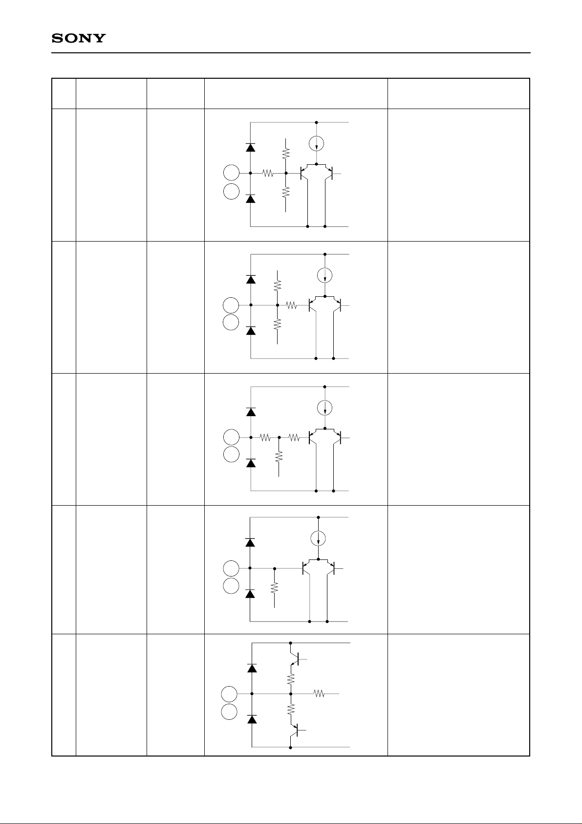
CXA1746Q
Pin
No. Pin voltage
30
29
7
8
Pin Name
TCMC21
TCMC11
TCMC22
TCMC12
I/O Resistance
4k
VCT
4k
VCT
29
Equivalent Circuit Description
V
CC
30
8
7
GND
V
CC
GND
Sets tone Mid frequency
Sets tone Mid frequency
9
28
10
27
TCLC21
TCLC11
TCLC22
TCLC12
8k
VCT
8k
VCT
28
10
27
V
CC
9
GND
V
CC
Sets tone Bass frequency
Sets tone Bass frequency
GND
V
CC
11
26
TCO2
TCO1
—
VCT
11
26
Tone control output
GND
—4—
CXA1746Q
Pin
No. Pin voltage
12
25
13
24
Pin Name
FDIN2
FDIN1
REO2
REO1
I/O Resistance
24k
VCT
—
VCT
12
25
Equivalent Circuit Description
V
CC
Fader input
GND
V
CC
13
24
GND
Rear output
14
23
15
FNT02
FNT01
TIMER
—
VCT
~
∞
—
14
23
15
V
CC
GND
V
CC
GND
V
CC
Front output
Sets timer constant
16
DATA
~
∞
—
16
Serial data input
GND
—5—
CXA1746Q
Pin
No. Pin voltage
17
18
19
20
21
Pin Name
VCT
CC
V
GND
DGND
CLK
I/O Resistance
—
VCT
—
VCC
—
Gnd
—
—
~
∞
—
21
Equivalent Circuit Description
CC
1/2 V
Power supply input
Ground
Digital ground
V
CC
Serial clock input
GND
22
1
36
37
38
47
49
39
40
41
42
43
44
45
46
CE
GAIN234
GAIN134
GAIN12
GAIN11
GAIN21
GAIN22
IN14
IN13
IN12
IN11
IN21
IN22
IN23
IN24
~
∞
—
~
∞
VCT
50k
VCT
39
41
43
45
22
36
37
38
47
48
V
CC
Latch enable input
GND
V
CC
1
External gain setting
for input amplifier
GND
V
CC
40
42
44
46
GND
Signal input
—6—
 Loading...