

Sony CXA1744AR Datasheet

CXA1744AR
For the availability of this product, please contact the sales office.
IF Amplifier for Digital Cordless Telephone
Description
The CXA1744AR is an IF amplifier IC designed for
digital cordless telephone of Europe, CT-2.
Features
• Mixer, RSSI, detector, and various other functions
required of a digital cordless phone IF amplifier.
• Local oscillator and multiplier for the mixer.
• Low power consumption (8.4mA at 3.0V)
• Small package (48-pin LQFP).
Absolute Maximum Ratings (Ta=25°C)
• Supply voltage VCC 14 V
• Operating temperature Topr –20 to +75 °C
• Storage temperature Tstg –65 to +150 °C
• Allowable power dissipation PD 500 mW
Structure
Bipolar silicon monolithic IC
Applications
Digital cordless telephone of Europe (CT-2)
48 pin LQFP (Plastic)
Recommended Operating Condition
• Supply voltage VCC 2.7 to 5.5 V
Sony reserves the right to change products and specifications without prior notice. This information does not convey any license by
any implication or otherwise under any patents or other right. Application circuits shown, if any, are typical examples illustrating the
operation of the devices. Sony cannot assume responsibility for any problems arising out of the use of these circuits.
—1—
E93Z33-TE
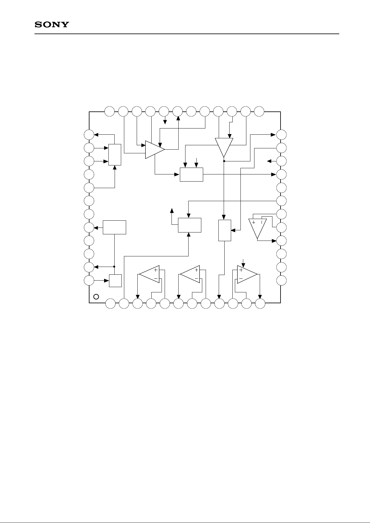
Block Diagram and Pin Configuration
CC
CXA1744AR
MIXOUT
MIXIN2
MIXIN1
BUFPAS
LOIN
REF
NC
MULTIOUT
NC
NC
OSCC
OSCB
37
38
39
40
41
42
43
44
45
46
47
48
MIXV
MIX
MULTI
OSC
IFP1
IFIN
IFP2
IF
SAMPLE
IFOUT
OPAMPCOMP1
RSSIVcc
RSSIOST
RSSI
REG
IFCNT
LIMP1
LIM
DET
LIMIN
SAMPLE
LIMP2
252627282930313233343536
COMP2
RSSIGND
COMP3
LIMOUT
24
QDIN
23
RSSIOST
22
RSSIOUT
21
REGOUT1
20
CC
V
19
FCOMPIN
18
FCOMPINX
17
FCOMPOUT
16
VREF
15
CURREF
14
GND
13
1 2 3 4 5 6 7 8 9
PSX
MIXGND
DCOMPINX
DCOMPOUT
OPOUT
DCOMPIN
OPINX
OPIN
10 11 12
DETOUT
ICOMPIN
ICOMPINX
ICOMPOUT
—2—
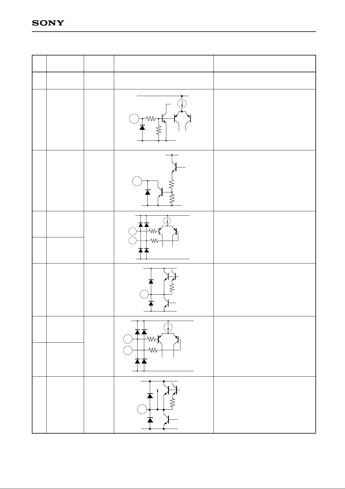
Pin Description
CXA1744AR
Pin Typical pin
No. voltage
Symbol Equivalent circuit Description
1 MIXGND 0V
2 PSX 0V
3 DCOMPOUT —
4 DCOMPINX —
5 DCOMPIN
GND for the MIX, OSC, and MULTI
circuits.
VCC
Power save control.
Power save mode for Low; power
32k
2
32k
GND
VCC
3
GND
VCC
4
5
129
129
save function executes on all circuits
except the OSC circuit and a part of
the REG circuit.
Data slicer comparator output.
Data slicer comparator input.
DCOMPINX is for out-of-phase
input.
DCOMPIN is for in-phase input.
6 OPOUT —
7 OPINX —
8 OPIN
9 DETOUT 1.25V
GND
VCC
6
GND
VCC
Operational amplifier output.
Operational amplifier input.
OPINX is for out-of-phase input.
7
129
129
8
GND
VCC
9
OPIN is for in-phase input.
Detector output.
—3—
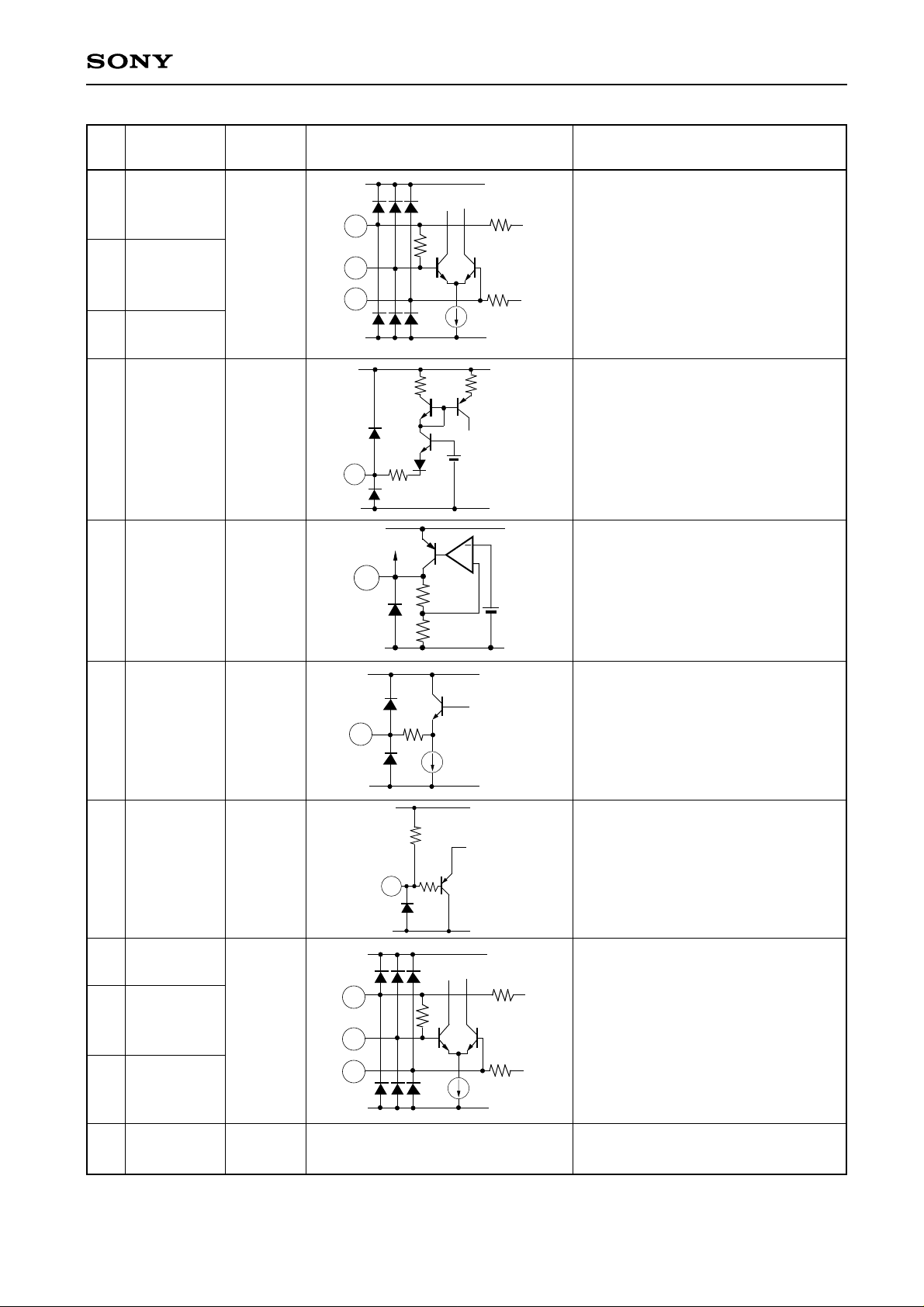
GND

CXA1744AR
Pin Typical pin
No. voltage
Symbol Equivalent circuit Description
10 ICOMPIN —
11 ICOMPINX
12 ICOMPOUT —
13 GND 0V
14 CURREF 1.25V
15 VREF 1.9V
VCC
Sample-and-hold circuit input.
ICOMPIN is for in-phase input.
10
11
12
129
129
CC
V
GND
GND
ICOMPINX is for out-of-phase input.
Sample-and-hold circuit output.
GND for circuits other than the MIX,
OSC, MULTI, and RSSI circuits.
V
CC
Adjustment for RSSI output current.
Connects a resistor between this pin
129
14
1.25V
GND
VCC
and GND.
Reference voltage.
Leave this pin open normally.
15
16 FCOMPOUT —
17 FCOMPINX —
18 FCOMPIN
16
1.25V
GND
VCC
Comparator output for free-channel
detection.
GND
VCC
129
17
129
18
GND
Comparator input for free-channel
detection.
FCOMPINX is for out-of-phase input.
FCOMPIN is for in-phase input.
—4—

CXA1744AR
Pin Typical pin
No. voltage
Symbol Equivalent circuit Description
19 VCC 3.0V
20 REGOUT1 1.25V
21 RSSIOUT —
22 RSSIOST 1.25V
20
22
21
129
129
129
VCC
1.25V
GND
RSSIVCC
GND
RSSIVCC
1.9V
Power supply for circuits other than the
MIX, OSC, MULTI, and RSSI circuits.
Internal bias regulator output.
A stabilized bias voltage can be
obtained.
RSSI current output.
A voltage output is obtained when a
resistor is connected between this pin
and GND.
RSSI offset adjustment.
The offset amount of RSSI output
current can be adjusted by connecting
a resistor between this pin and GND.
23 QDIN 2.45V
24 LIMOUT 1.55V
25 RSSIGND 0V
RSSIVCC
32k
23
129
GND
RSSIVCC
24
GND
Detector input.
Connect a detection discriminator.
Limiter output.
GND for the IF amplifier, limiter and
RSSI circuits.
—5—
CXA1744AR
Pin Typical pin
No. voltage
Symbol Equivalent circuit Description
26 LIMP2 1.5V
27 LIMIN
28 LIMP1
29 IFCNT 0.6V
30 RSSIVCC 2.45V
31 IFOUT 1.55V
28
27
26
29
30
129
460
1.9V
+
RSSIV
50k
50k
GND
RSSIVCC
GND
V
1.25V
GND
RSSIVCC
CC
CC
Limiter input. Input the signal from IF
amplifier to LIMIN. Connect a
decoupling capacitor to LIMP1 and
LIMP2.
IF amplifier gain adjustment.
Connect a resistor between this pin
and GND to compensate for the
interstage filter insertion loss between
the IF amplifier and limiter.
Power supply for the IF amplifier,
limiter and RSSI circuits.
Connected to the regulator output
internally.
Connect a decoupling capacitor.
IF amplifier output.
32 SAMPLE 3.0V
33 IFP2 1.55V
34 IFIN
35 IFP1
36 MIXVCC 3.0V
35
34
33
31
420
GND
VCC
50k
Sample-and-hold circuit control input.
Sample mode for open or High; hold
mode for Low.
10k
32
GND
RSSIV
50k
CC
IF amplifier input. Input the signal
from MIX to IFIN. Connect a
decoupling capacitor to IFP1 and
330
50k
GND
IFP2.
Power supply for the MIX, OSC, and
MULTI circuits.
—6—
 Loading...