

Sony CXA1742Q Datasheet

CXA1742Q
For the availability of this product, please contact the sales office.
IF Amplifier for Analog Cellular Communications
Description
The CXA1742Q is an analog cellular(AMPS) FM IF
IC which include an IF filter.
Features
• Include a ceramic filter function, which is normally
mounted externally.
• Quadrature detection discriminator function.
• This IC has almost all IF functions and is ideal for
reduction in set size because of few external parts
required.
• Channel filter conforming to the AMPS standard.
• Wide operating voltage range (2.7 V to 3.6 V) and
low current consumption (Icc=10 mA (typ.) when
Vcc= 3 V).
• Wide range and excellent temperature
characteristics for the RSSI (receiving signal
strength indicator).
Absolute Maximum Ratings (Ta = 25°C)
• Supply voltage VCC 5V
•Operating temperature Topr –35 to +85 °C
• Storage temperature Tstg –65 to +150 °C
• Allowable power dissipation
Operating Conditions
Supply voltage VCC 2.7 to 3.6 V
40 pin QFP (Plastic)
PD 500 mW
Applications
Ideally suited for cellular phones, particularly handheld sets.
Structure
Bipolar silicon monolithic IC
Sony reserves the right to change products and specifications without prior notice. This information does not convey any license by
any implication or otherwise under any patents or other right. Application circuits shown, if any, are typical examples illustrating the
operation of the devices. Sony cannot assume responsibility for any problems arising out of the use of these circuits.
—1—
E95119-TE
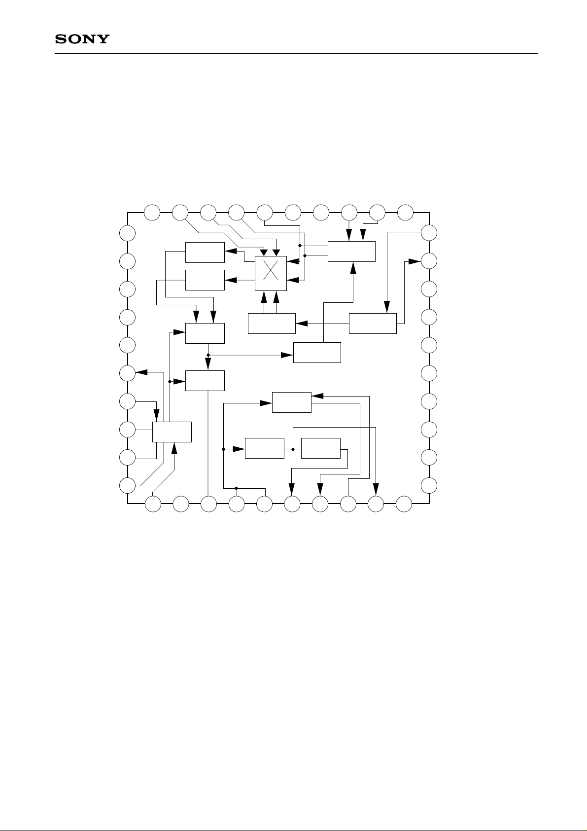
Block Diagram and Pin Configuration
CXA1742Q
(Top View)
T4
T5
CC1
V
GND1
T6
FADJ1
FADJ2
SGND
BPFPS1
31
32
33
34
35
36
37
38
39
T3
BIAS
MIXADJ1
PSN
PSN
BPF0
BPF1
MIXADJ2
MIXPS
MIXIN
MIXER
1/
2
LIM DET
RSSI
GND
AGC
CC
V
IFPS
23 22 212425262730 2829
RF AMP
OSC
IFIN
GND
20
19
18
17
16
15
14
13
12
XTALIN
XTALOUT
AGCPS
VREF
RSSIPS
T2
RSDETPS
T1
GND2
BPFPS2
40
1 2 3 4 5 6 7 8 9
NC
SW
BPFO
LIMIN
AUDIO
RSSI
10
IF2
LIMPS
GADJ(RSSI)
11
CC2
V
Note) Pins 21 and 25 are connected via the IC internal wiring.
Pins 12, 21 and Pins 25, 34 are connected via IC internal resistors.
When designing a PCB, ensure that all GND pins of IC are connected to the GND on PCB with its
connection wiring distance minimized.
—2—
CXA1742Q
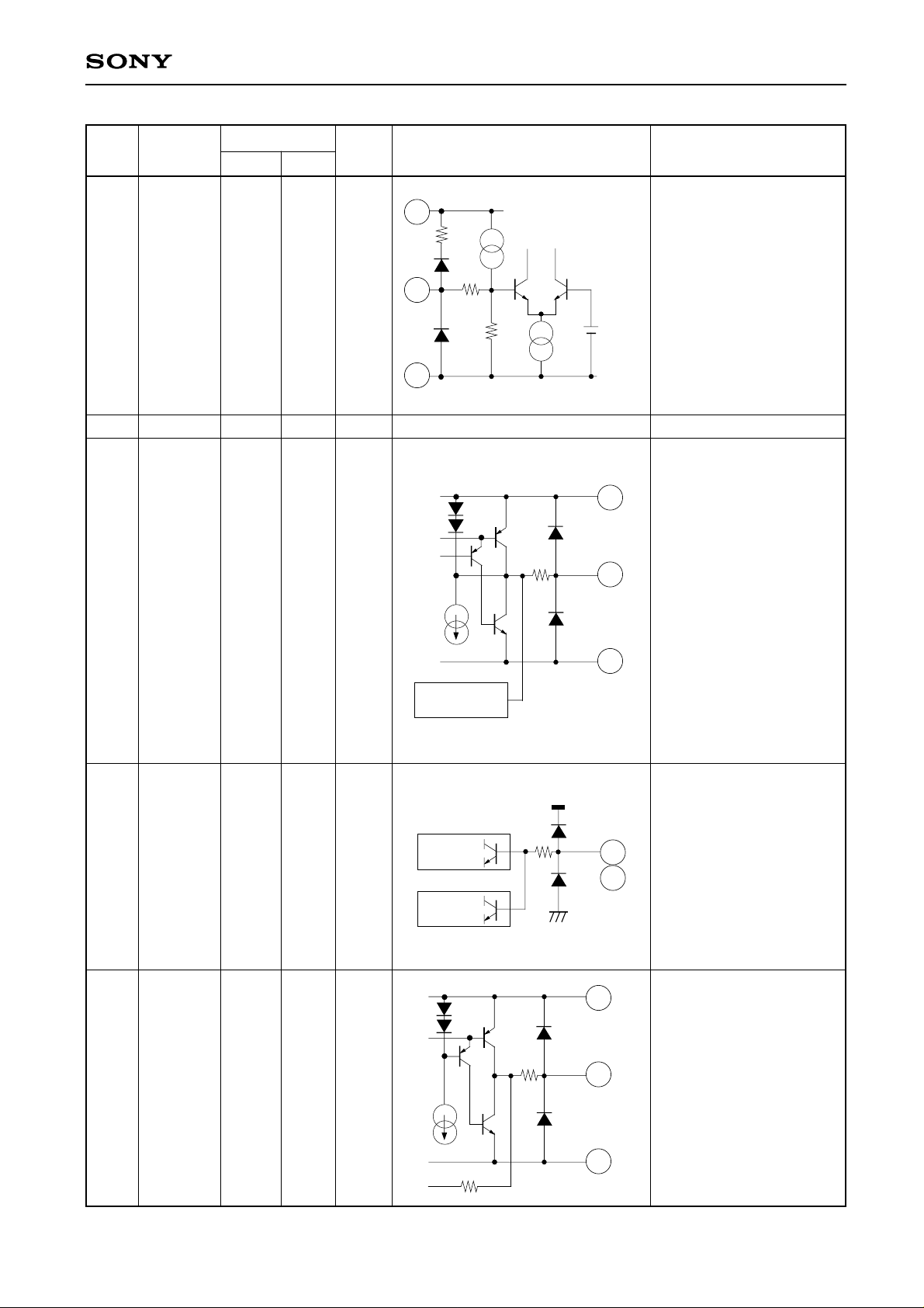
Pin No. Symbol
1SW
2NC
3 BPFO 1.83V
Pin voltage I/O
DC AC
resistance
31
34
Equivalent circuit Description
Used at the GND potential.
20µA
50k
1
50k
VREF
GND
Not intemally connected.
BPF output.
Connect to Pins 4,5.
33
147
3
4 LIMIN Open
5 Base
6 AUDIO 1.85V
B.P.F
N.F.B Network
LIM
RSSI
1k
147
11
34
Input of BPF output.
The DC bias is applied
from pin3 when the output
of BPF is connected to
4
them.
5
Outputs an AUDIO signal
which is FM-detected.
6
—3—
12

CXA1742Q
Pin No. Symbol
7 RSSI 1.1 V
8 GADJ 0.2 V
Pin voltage I/O
DC AC
resistance
Equivalent circuit Description
RSSI output. Outputs a
11
DC voltage in accordance
with the signal input to the
RF amplifier.
147
7
12
Adjusts the RSSI amplifier
gain.
8
147
147
7
9 IF2 1.07 V
10 LIMPS 1.82 V
147
11
12
Limiter operation monitor.
Not used normally.
9
Connects a limiter
11
integrating capacitor.
10
—4—
12
CXA1742Q
Pin No. Symbol
11 VCC2 3.0 V
12 GND2 0 V
13 T1
14 RSDETPS 1.35 V
15 T2
Pin voltage I/O
DC AC
resistance
Equivalent circuit Description
Power supply. Supplies
current to the LIM, DET,
and RSSI circuits.
Ground.
IC operation check.
Connects an RSSI detector
integrating capacitor.
11
147
14
12
IC operation check.
16 RSSIPS 1.83 V
17 VREF 1.25 V
reference voltage
used in the
internal circuit
11
16
12
Connects an RSSI
integrating capacitor.
Monitor for the reference
33
voltage used in the internal
circuit.
17
When connected to an
external capacitor, this pin
also functions to lower the
reference voltage dynamic
impedance.
34
—5—

CXA1742Q
Pin No. Symbol
18 AGCPS 0.233 V
19 XTALOUT
20 XTALIN 2.96 V
Pin voltage I/O
DC AC
resistance
VREF
20
Equivalent circuit Description
Connects an AGC
33
integrating capacitor.
18
34
15
Connect a crystal oscillator
to form a Colpitts-type
24
147
10k
15p
10k
oscillator circuit.
When an external
oscillator is used, its signal
19
must be connected to Pin
20.
21 GND 0 V
22 IFIN 1.25 V
23 IFPS 1.25 V
24 VCC 3.0 V
25 GND 0 V
25
22
VREF
21
Ground.
RF amplifier input. The
relationship between IFIN
24
(Pin 22) and IFPS (Pin 23)
is designed so that the IC
internal stray capacitance
23
1.5k1.5k
is small.
Therefore, if Pins 22 and
23 are used for balance
input, the common-mode
2521
rejection deteriorates.
Power supply.
Supplies current to the RF
AMP, MIXER, OSC, and
1/2 DIVIDER circuits.
Ground.
—6—
 Loading...