

Sony CXA1737R Datasheet

CXA1737R
AFM Stereo Signal Processor for 8 mm VCR
Description
The CXA1737R is a bipolar IC designed as an
AFM stereo signal processor for 8mm VCR.
All functions necessary for AFM stereo are
concentrated onto a single 64-pin LQFP.
Features
• Low supply voltage (3.15V) design
• Low power consumption (Vcc = 3.15V)
Recording: 150mW
Playback: 240mW
• Built-in BPF (1.5MHz, 1.7MHz)
• Supports NTSC and PAL
• Enables both parallel and 3-line serial mode control
• Supports electronic volume (EVR) control
Structure
Bipolar silicon monolithic IC
Applications
8mm VCRs
64 pin LQFP (Plastic)
Absolute Maximum Ratings
• Supply voltage VCC 5.25 V
• Operating temperature Topr –20 to +75 °C
• Storage temperature Tstg –65 to +150 °C
• Allowable power dissipation
PD 1500 mW
Operating Conditions
• Recommended supply voltage
VCC 3.15 V
VCCH 4.75 V
• Supply voltage range VCC 3 to 5.25 V
VCCH 4.5 to 5.25 V
Sony reserves the right to change products and specifications without prior notice. This information does not convey any license by
any implication or otherwise under any patents or other right. Application circuits shown, if any, are typical examples illustrating the
operation of the devices. Sony cannot assume responsibility for any problems arising out of the use of these circuits.
– 1 –
E96Z11A77

Block Diagram
CXA1737R
LINEO L
EPOUT L
GNDH
EPLINEOUT R
MUTEOUT
V
MIXOUT
V
PMUTETC
MIC/LINE (CS)
REC/PB (CK)
LINE MIX ON/OFF(SI)
VCT5
MICIN L
V
LINEIN L
37
MONI L
AFLIM
LIM
LIM
AFLIM
DEVADJ L
36
PBREC
PBREC
LPF
PHASE
COMP
PHASE
COMP
LPF
MUTE
NC
35
DOC
DET
1.5MHz
VCO
LIM
MONO
LIM
1.7MHz
VCO
MUTE
DET
MUTE OFF
DELAY
PLLLPF L
34
OFF
LPF
1.5M
1.7M
1.7MHz
BFPRFAGC
1.5MHz
BFP
FWR
OUTSEL CTL (P.SAVE)
33
PLL L
MIX
PLL R
ONREC
MONO
DET
32
MATRIX CTL
RFSWP
31
NC
30
FSCIN
29
NTSC/PAL
28
27
MUTETC
26
BPF ADJ
VCT
25
RECFMOUT
24
BPFMONI
23
PBRFIN
22
RFAGCTC
21
MONOOUT
20
PLLLPF R
19
18
MONO DET
SI/PA (SP/LP)
17
PG
TCH L
39
DEC OUT
DEC IN
ENC OUT
ENC IN
TC L
38
NR R
45
L-OUT
R-OUT
REC
PB
PB
REC
REC
REC
NC
R-IN
PB
PB
SHTC L
44
PBREC
LPF
LPF
MUTE ON/OFF
48
LINE Lch
LINE
E.P.
E.P./
LINE
MUTE
MIX
CONTROL
BUS
DECODER
MIC
LINE
MIX
LINE
MIC
49
50
51
52
53
POWER
MUTE
CCH
54
55
CC2
56
57
58
59
60
61
62
63
CC1
64
OFFON
OUTSEL
ALC
DET
ALC
46
47
MUTE
MUTE
MATRIX
L-IN
PBREC
D.C.
D.C.
FADE
FADE
SHTC R
DC R
WEIGHT L
VCTH
43
42
DEC IN
DEC OUT
ENC IN
ENC OUT
REC
PB
PB
REC
41
NR L
LPEMP
S/H
S/H
LPEMP
NRDC L
GND2
40
LP
D.C.
MUTE
SP
OR
DOUB
SP
D.C.
MUTE
LP
1
ALCDET
2
LINEIN R
4
3
FADE
MICIN R
IFDC R
IREF
7
RFDC L
6
5
8
RFDC R
9
IFDC L
10
11
GND1
WEIGHT R
12
NRDC R
13
TCH R
14 15
TC R
MONI R
16
DEVADJ R
– 2 –

CXA1737R
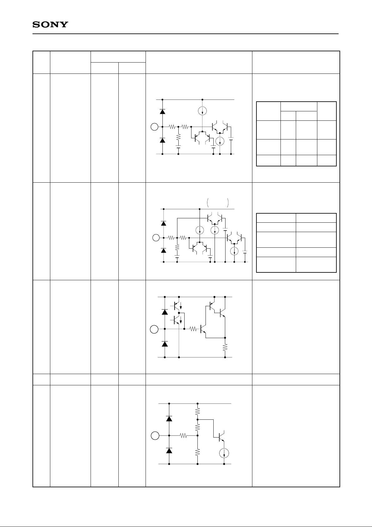
Pin Description (VCC1, VCC2 = 3.15V, VCCH = 4.75V, Ta = 27°C)
Pin
No.
Symbol Equivalent circuit Description
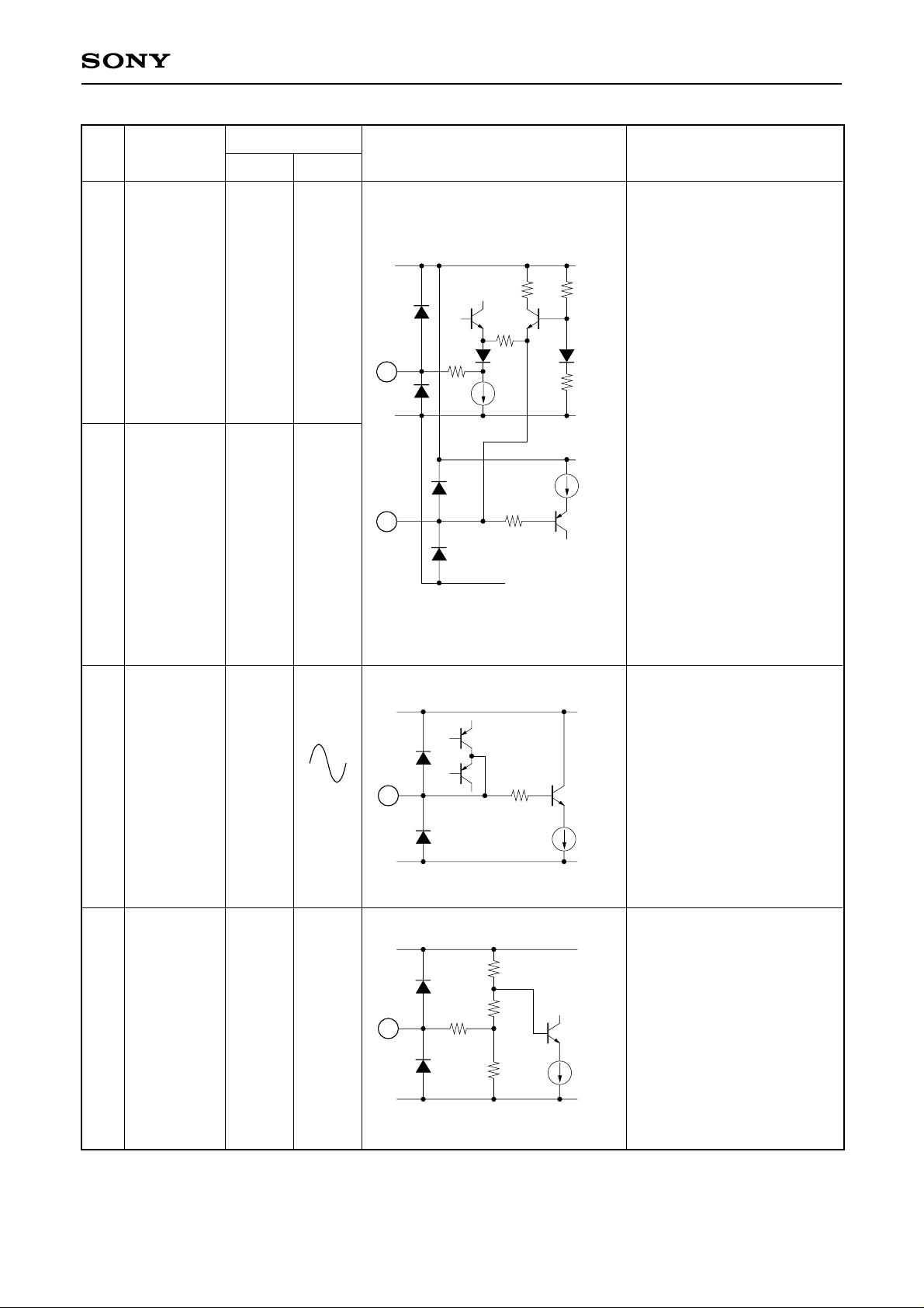
1 ALCDET
2 LINEIN R
Pin voltage
DC AC
——
1.23V
Reference
input
–38dBm
∗
1
Vcc1
2µ
ALC time constant pin.
250500
1
1k
Vcc1
ALC is OFF when this pin is
low.
GND
Line input pin. Standard input
5µ
level: –38dBm.
This pin has a small input
2
147
50k
signal level and high input
impedance. Therefore, be
careful not to cause cross
VCT = 1.23V
GND
talk with other signals.
3 FADE
4 MICIN R
See
Graph 1.
1.23V
—
Reference
input
–38dBm
∗
1
Vcc1
20µ
EVR control pin for fader.
0 to 0.5V with fixed gain.
3
50k
50k
Increasing the applied
voltage lowers the gain and
causes the fader to operate.
1.24V
GND
Vcc1
Microphone input pin.
5µ
Standard input level: –38dBm.
This pin has a small input
4
147
50k
signal level and high input
impedance. Therefore, be
careful not to cause cross
VCT = 1.23V
GND
talk with other signals.
– 3 –
∗1
0dBm = 2.19Vp-p

CXA1737R
Pin
No.
Symbol Equivalent circuit Description
5 IFDC R
6 IREF
Pin voltage
DC AC
1.90V —
1.17V —
VccH
DC monitor pin of Rch signal
5
1k
40k
40µ
GND
Vcc1
path.
Pin for generating the
reference current. Connect a
192
6
192
GND
47kΩ external resistor to
GND. Be careful not to cause
pin cross talk.
7 RFDC L
8 RFDC R
1.91V —
1.91V —
Vcc1
26.8k
DC monitor pin of Lch signal
path.
7
8
1k
26.8k
1k
60µ
GND
Vcc1
DC monitor pin of Rch signal
path.
60µ
GND
– 4 –

CXA1737R
Pin
No.
Symbol Equivalent circuit Description
9 IFDC L
10 GND1
11 WEIGHT R
Pin voltage
DC AC
1.90V —
∗1
0V
—
1.23V —
11
VccH
9
1k
40k
40µ
GND
—
VCC1
5µ
DC monitor pin of Lch signal
path.
Audio system GND pin.
NR WEIGHT time constant
4.7k
pin.
12 NRDC R
1.73V —
12
147
1k
GND
VCC1
5µ
GND
DC offset cancel pin of NR
block.
∗
1
Externally applied voltage
– 5 –
CXA1737R
Pin
No.
Symbol Equivalent circuit Description
Pin voltage
DC AC
13 TCH R 0.56V —
14 TC R 1.19V —
13
14
147
150
10µ
1k
200
VCC1
GND
2µ
NR attack/ recovery time
constant pins.
15 MONI R
16 DEVADJ R
1.89V
See
Graph 4.
Reference
output
–15dBm
∗
1
—
15
16
60k
47k
3k
50k
1k
VCC1
Pin for monitoring the signal
before modulation during
recording and after
demodulation during
playback of Rch.
30µ
GND
VCC1
Deviation adjusting pin.
The variable width is from
0 to Vcc.
20µ
GND
– 6 –
∗1
0dBm = 2.19Vp-p
CXA1737R
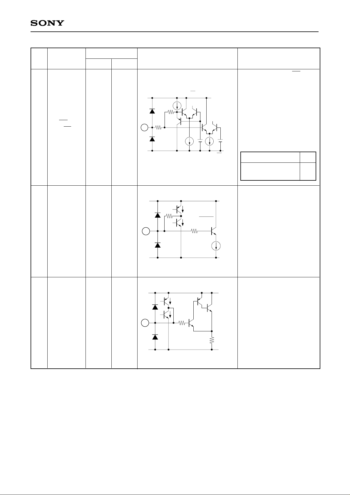
Pin
No.
17
Symbol Equivalent circuit Description
SI/ PA
(SP/ LP)
18 MONO DET
Pin voltage
DC AC
——
2.47V —
17
18
147
50k
1k
SP/LP
1.5V
20µ
10µ
during MONO
2µ
during MONO
0.5µ
10k
VCCH
4V
GND
SI/PA SW
VCC1
Serial/ parallel (SP/ LP) mode
switching pin. When this pin
is 4.3V or more, the IC
operates in serial control
mode and mode control for
the IC is performed by CS,
CK and SI of Pins 58, 59 and
60. When this pin is 3.5V or
less, the IC operates in
parallel control mode as
follows.
L (0 to 1V) LP
H (2 to 3.5V)
or OPEN
SP
MONO DET time constant
pin.
19 PLLLPF R
——
19
0.08µ
0.08µ
1k
25k
10µ
GND
VCC2
GND
PLL time constant pin. Since
this pin has a small attraction
and discharge current,
signals should be received
with high impedance when
monitoring this pin. Also, be
careful not to cause pin cross
talk.
– 7 –

CXA1737R
Pin
No.
Symbol Equivalent circuit Description
20 MONOOUT
Pin voltage
DC AC
——
20
MONODET OUT
5k
5k
STEREO: H
MONO: L
VCC1
1V
20µ
GND
Bil Rec CTL IN
MONODET discrimination
output pin. This pin is open
collector, and it is pulled up to
Vcc with 100kΩ resistor.
During parallel mode, this pin
is also recording bilingual
control input pin.
• Specification for parallel CTL
During recording:
Bilingual recording
mode when this pin
is set to low (0 to 1 V)
during low of Pin 32
(REC MONO mode).
During playback:
Outputs MONO
discrimination result.
Open for MONO;
Low for others.
• Specification for serial CTL
See Mode Control Tables of
3) SO control mode table.
21 RFAGCTC
22 PBRFIN
2.48V —
—
Reference
input AFM
15mVp-p
(1.5MHz)
21
22
VCC – 1.1V
V
CC – 1.15V
17k147
1k
17k
50µ
VCC2
RFAGC time constant pin.
40µ
GND
VCC2
Input pin for PB RF signal.
The reference input level is
approximately 200mVp-p
(Y + C + AFM).
Note that the reference input
level of AFM 1.5MHz
component is 15mVp-p.
GND
– 8 –
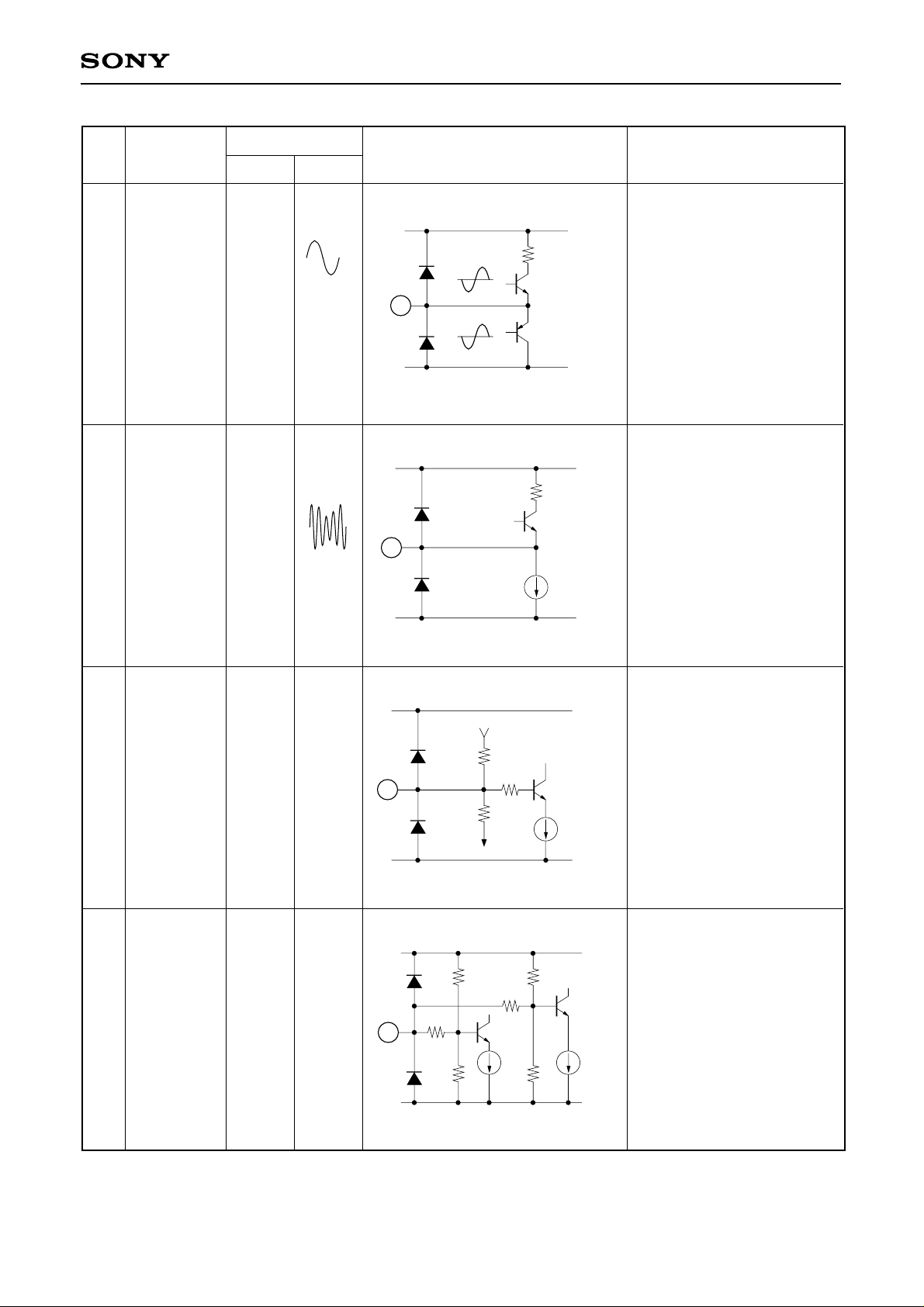
CXA1737R
Pin
No.
Symbol Equivalent circuit Description
23 BPFMONI
24 RECFMOUT
Pin voltage
DC AC
During
1.5M BPF
monitoring
1.09V
During
1.7M BPF
monitoring
2.51V
0.96V
Reference
output
1.5M BPF
= 180mVp-p
1.7M BPF
= 190mVp-p
1.5M + 1.7M
reference
output
24
1.5M BPF OUT 100
23
1.7M BPF OUT
100
220µ
VCC2
GND
VCC2
GND
This pin is for measurement
which monitors the BPF
output.
For monitoring 1.5M BPF
characteristics, connect 4.7kΩ
resistor to GND.
For monitoring 1.7M BPF
characteristics, connect 4.7kΩ
resistor to Vcc.
Recording FM modulated
output pin. Reference output
is 220mVp-p for 1.5M
component; 175mVp-p for
1.7M component.
25 VCT
26 BPF ADJ
1.89V —
See
Graph 2.
—
25
26
60k
60k
23k
1k
47k
73k 73k
47k
23k
20µ
VCC1
IC internal bias pin. Connect
a decoupling capacitor.
50µ
GND
VCC2
Pin for varying the BPF fo.
The variable width is 0 to Vcc.
20µ
GND
– 9 –
CXA1737R
Pin
No.
Symbol Equivalent circuit Description
27 MUTETC
28
NTSC/ PAL
Pin voltage
DC AC
2.43V —
——
28
27
50k
1k
during DOC
0.6µ
during DOC
2.5µ
10k
40µ
1.5V
VCC1
10µ
GND
VCC1
GND
Time constant pin for
determining the MUTE OFF
delay time.
MUTE ON when drop out (T)
continues approximately 1ms
(during 680pF externally).
Pin 22 input
Pin 27
T
VTH
MUTE ON
NTSC/PAL switching pin
during parallel mode.
L (0 to 1V)
PAL
H (2V to VCC) NTSC
29 FSCIN
1.68V
Reference
input
200mVp-p
30 NC ———
31 RFSWP
—
Reference
input
30Hz
31
29
147
V
CC – 1.4V
147 50k
40k
110k
1.2V
VCC2
fsc input pin.
The input level is
approximately 200mVp-p.
During NTSC: 3.579545MHz
During PAL: 4.433619MHz
20µ
GND
VCC1
RFSWP input pin.
H (2V to Vcc)
L (0 to 1V)
30Hz
GND
– 10 –
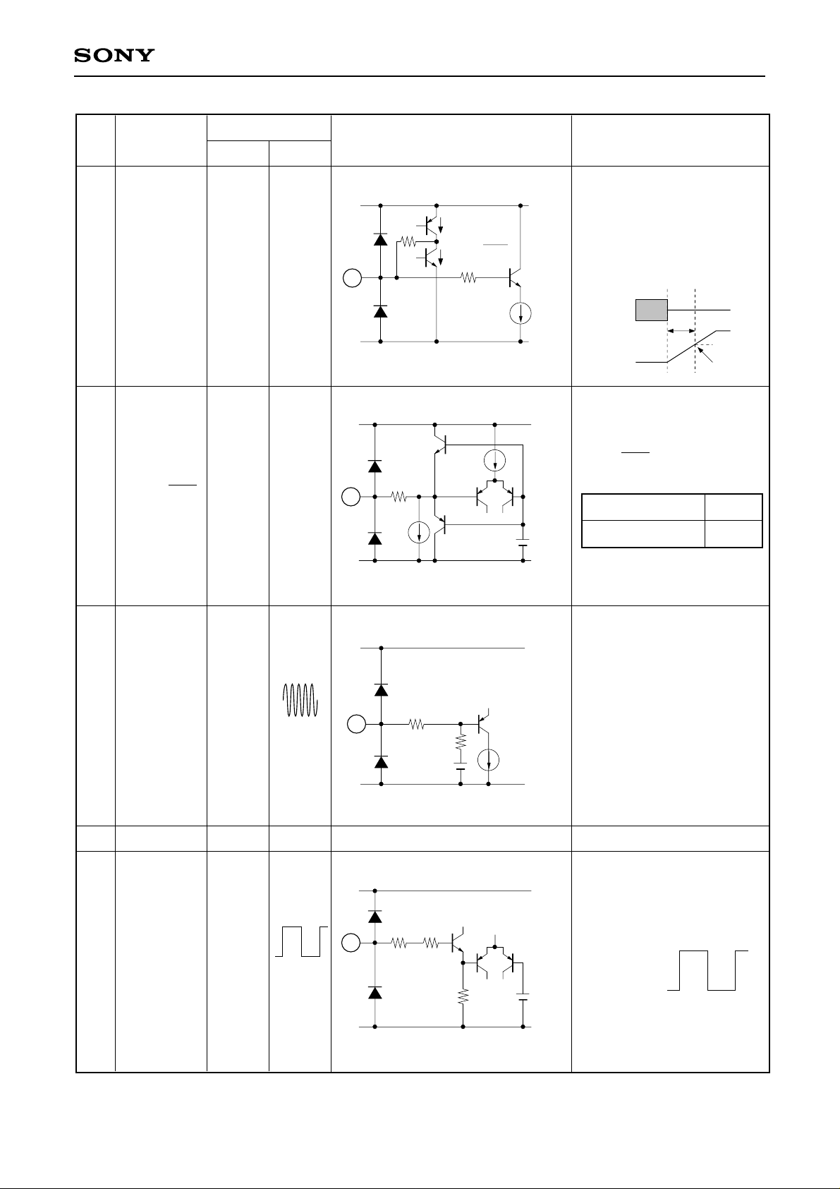
CXA1737R
Pin
No.
32
33
Symbol Equivalent circuit Description
Pin voltage
DC AC
MATRIX control input pin
during parallel mode.
VCC1
During parallel
REC
MONO
STEREO
CC)
STEREO
MATRIX CTL
——
32
147 50k
50k
10µ
Pin 32
L (0 to 0.7V)
2V
1V1.5V
10µ
GND
M (1.3 to 1.7V)
or OPEN
H (2.3V to V
OUTPUT SEL control input
OUTSEL CTL
(P.SAVE)
VCC2
——
GND
33
147 50k
50k
10µ
10µ
1V1.5V
BPF OFF
P.SEVE
4V
CTL SW
10µ
pin during parallel mode.
Pin 33
L (0 to 0.7V)
M (1.3 to 1.7V)
or OPEN
2V
H (2.3 to 3.5V)
H2 (4.3V to V
CCH)
During
serial
PB
Bilingual/
MONO Auto
STEREO/
MONO Auto
STEREO
Lch/ Rch
Lch/ Rch (Main)
Lch/ Rch (SUB)
Power save
1.5M BPF through
REC
MONO
—
—
Mode
34
PLLLPF L
35 NC
DEVADJ L
36
1.75V —
——
See
Graph 3.
—
34
36
0.08µ
60k
0.08µ
1k
47k
3k
50k
25k
20µ
VCC2
GND
VCC1
GND
PLL time constant pin. Since
this pin has a small attraction
and discharge current,
signals should be received
with high impedance when
monitoring this pin. Also, be
careful not to cause pin cross
talk.
—
Deviation adjusting pin.
The variable width is from
0 to Vcc.
– 11 –
 Loading...