

Sony CXA1720Q Datasheet
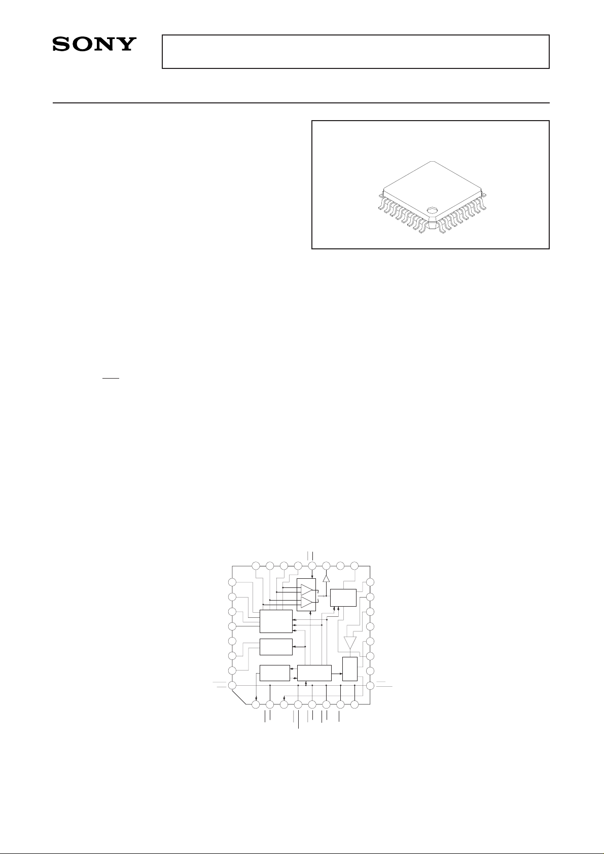
Block Diagram and Pin Configuration
—1—
E93717-TE
Read/Write Amplifier (with Built-in Filters) for FDDs
32 pin QFP (Plastic)
CXA1720Q
• Supply voltage detection circuit prohibits error
writing during power ON/OFF or abnormal voltage.
• Power consumption is kept down to 115 mW (typ.)
and this IC is suitable for use with battery-driven
FDDs.
• Built in Time constant capacitors for monostable
multivibrator Nos. 1 and 2. (The pulse width for
monostable multivibrator No. 2 is fixed.)
• Power saving function reduces power consumption
when the IC is not in use. When in power saving
mode (5 mW typ.), only the power supply ON/OFF
detector functions.
• The Write driver has a built-in reset circuit. When
the mode is switched from Read mode to Write
mode, the Write current flows from head 0A if head
side 0 is selected and from head 1A if head side 1
is selected.
Description
The CXA1720Q is an IC for use with floppy disk
drives, and contains a Read circuit (with built-in
filters), Write circuit, Erase circuit, and supply
voltage detection circuit, all into a single chip.
Features
• Single 5 V power supply.
• Filter system can be switched among four modes:
1M/2M, and inner track/outer track. This allows for
a significant reduction in the number of external
parts such as differentiator constants, low-pass
filters, and switches. (Compared with conventional
Sony products, the number of parts has been
reduced by one-half.)
• Filter characteristics can be customized.
• Low pre-amplifier input conversion noise voltage of
2.0 nV/ √ Hz (typ.) keeps Read data output jitter to
a minimum. The pre-amplifier voltage gain can be
selected as either 100× or 200×.
• The monostable multivibrator No. 1 pulse width
switching function for the time domain filter permits
switching between 1M and 2M mode.
• Write current switching function permits switching
of the Write current among four modes: 1M/2M
and inner track/outer track. (Filter inner track/outer
track switching is separate.)
FILTER
OUT B
COMP
IN B
COMP
IN A
A.GND
MMVA
FILTER
SET
Vcc
HIGH
DENSITY
POWER
ON
WRITE
DATA
READ
DATA
WRITE
CURRENT
WRITE
GATE
ERASE
GATE
SIDE 1
FILTER
CONTROL
W/C 1
SET
W/C 1
COMP
W/C 2
SET
W/C 2
COMP
ERASE
OUT 0
ERASE
OUT 1
HEAD 0A
HEAD 0B
HEAD 1A
HEAD 1B
PREAMP
OUT
VREF
FILTER
OUT A
WRITE
DRIVER
ERASE
DRIVER
POWER
MONITOR
CONTROL
LOGIC
TIME
DOMAIN
FILTER
COMP
FILTER
DIFF+LPF
(BPF)
1 2 3 4 5 6 7 8
16
15
14
13
12
9
10
11
22 21 20 19 18 172324
HIGH
GAIN
25
26
27
28
29
30
31
32
D.GND
POWER
SAVE
PREAMP
Sony reserves the right to change products and specifications without prior notice. This information does not convey any license by
any implication or otherwise under any patents or other right. Application circuits shown, if any, are typical examples illustrating the
operation of the devices. Sony cannot assume responsibility for any problems arising out of the use of these circuits.
For the availability of this product, please contact the sales office.

—2—
CXA1720Q
Structure
Bipolar silicon monolithic IC
Absolute Maximum Ratings (Ta=25 °C)
• Supply voltage VCC 7 V
• Digital signal input pin (note) input voltage –0.5 to VCC+0.3 V
• Power ON output applied voltage VCC+0.3 V
• Erase output applied voltage VCC+0.3 V
• Head 0A, 0B, 1A, 1B applied voltage 15 V
• Power ON output sink current 7 mA
• Erase output sink current 30 mA
• Operating temperature Topr –20 to +75 °C
• Storage temperature Tstg –65 to +150 °C
• Allowable power dissipation PD 500 mW
Supply Voltage Range
VCC 4.4 to 6.0 V
Note) WRITE DATA, WRITE CURRENT, WRITE GATE, ERASE GATE
SIDE1, FILTER CONTROL, HIGH DENSITY, HIGH GAIN, POWER SAVE

—3—
CXA1720Q
Pin Description (Ta=25 °C, VCC=5 V)
Vcc
A.GND
1k
2
2.3V
Vcc
D.GND
140
3
Vcc
A.GND
1k
100k
2.1V
4
5
6
8
9
20
7
Pin
Symbol Pin voltage Equivalent circuit Description
No.
1
2
3
4
5
6
7
8
9
20
POWER ON
WRITE
DATA
READ
DATA
WRITE
CURRENT
WRITE
GATE
ERASE
GATE
SIDE1
FILTER
CONTROL
HIGH
DENSITY
HIGH
GAIN
—
—
—
—
—
—
—
—
—
—
Vcc
A.GND
100k
1
Reduced voltage detection output.
This is an open collector that outputs a low signal
when VCC is below the specified value.
Write data input.
This pin is a Schmitt-type input and is triggered
when the logical voltage goes from high to low.
Read data output.
This pin is active when the logical voltage of the
Write gate signal and the Erase gate signal is high.
Write current control. The Write current is
increased when the logical voltage is low.
Write gate signal input. The Write system is active
when the logical voltage is low.
Erase gate signal input. The Erase system is
active when the logical voltage is low.
Head side switching signal input. The HEAD1
system is active when the logical voltage is low,
and the HEAD0 system is active when the logical
voltage is high, but only when the logical voltage
for the Write gate and the Erase gate is high.
Filter inner track/outer track mode control. Inner
track mode is selected when the logical voltage is
low.
Filter, time domain filter and Write current 1M/2M
mode control. 2M mode is selected when the
logical voltage is low.
Pre-amplifier voltage gain selection. Gain of 100x
is selected when the logical voltage is high; gain of
200x is selected when the logical voltage is low.

—4—
CXA1720Q
Pin
Symbol Pin voltage Equivalent circuit Description
No.
10
11
12
13
14
15
16
17
VCC
FILTER
SET
MMVA
A. GND
COMP IN A
COMP IN B
FILTER
OUT B
FILTER
OUT A
—
3.8 V
0.5 V
—
3.3 V
3.3 V
3.3 V
3.3 V
Vcc
A.GND
147
11
1.2V
1k
Power supply (5 V) connection.
Connection for filter cut-off frequency setting
resistor. Connect the filter cut-off frequency setting
resistor RF between this pin and VCC to set the cutoff frequency.
Time domain filter monostable multivibrator No. 1
pulse width setting pin. Connect the monostable
multivibrator No. 1 pulse width setting resistor RA
between this pin and A.GND.
Analog system GND connection.
Comparator differential inputs.
Filter differential outputs.
Vcc
147
12
1.2V
A.GND
10k
10k
16k
Vcc
14
15
140
500µ
147
147
140
500µ
60µ
A.GND
Vcc
16
17
A.GND
—5—
CXA1720Q
Pin
Symbol Pin voltage Equivalent circuit Description
No.
18
19
21
22
23
24
25
27
26
28
VREF
PREAMP
OUT
HEAD 1B
HEAD 1A
HEAD 0B
HEAD 0A
W/C1SET
W/C2SET
W/C1
COMP
W/C2
COMP
2.8 V
2.8 V
—
—
—
—
—
—
Vcc
A.GND
500
120µ
18
Connection for internal reference voltage
decoupling capacitor. Connect the decoupling
capacitor CREF between this pin and A.GND.
Pre-amplifier output.
Connection for magnetic head input/output.
Connect the recording/playback magnetic head to
these pins, and connect the center tap to VCC.
When the logical voltage for Pin 7 (SIDE1) is low,
the HEAD1 system is active; when the logical
voltage is high, the HEAD0 system is active.
Connection for 1M write current setting resistor.
Connect the Write current setting resistor RW1
between this pin and VCC to set the Write current.
Connection for 2M Write current setting resistor.
Connect the Write current setting resistor RW2
between this pin and VCC to set the Write current.
Connection for 1M Write current compensation
resistor.
Connect the Write current compensation resistor
RWC1 between this pin and Pin 25 (W/C1SET) to
set the amount of increase in the Write current.
Connection for 2M Write current compensation
resistor.
Connect the Write current compensation resistor
RWC2 between this pin and Pin 27 (W/C2SET) to
set the amount of increase in the Write current.
140
Vcc
19
320µ
24
23
22
21
A.GND
A.GND
Vcc
1.2V
147
147
25
27
A.GND
Vcc
26
28
A.GND

—6—
CXA1720Q
Pin
Symbol Pin voltage Equivalent circuit Description
No.
29
30
31
32
D. GND
ERASE
OUT0
ERASE
OUT1
POWER
SAVE
—
—
—
—
Vcc
D.GND
30
31
Digital system GND connection.
Erase current output for the HEAD0 system.
Erase current output for the HEAD1 system.
Power saving signal input.
When the logical voltage is low, the IC is in power
saving mode. In power saving mode, only the
power supply ON/OFF detection function operates.
162k
1k
32
Vcc
2.1V
A.GND
—7—
CXA1720Q
Electrical Characteristics
Current Consumption (Ta=25 °C, VCC=V)
Power Supply Monitoring System (Ta=25 °C)
Read System
∗When SW4 = a: Vi = 10 mVp-p
When SW4 = b: Vi = 5 mVp-p
Measure- Measure-
Item Symbol Conditions ment ment Min. Typ. Max. Unit
circuit point
Current consumption for Read ICCR
V
CC=5 V
— — 13.0 23.0 33.0
WG=“H”
Current consumption for
ICCWE
V
CC=5 V
— — 8.0 14.0 20.0 mA
Write/Erase WG=“L”, EG=“L”
Current consumption for
ICCPS
V
CC=5 V
— — 0.9 1.8
Power saving PS=“L”
Measure- Measure-
Item Symbol Conditions ment ment Min. Typ. Max. Unit
circuit point
Power supply ON/OFF detector
VTH — — 3.5 3.9 4.3
threshold voltage
V
Power ON output saturation
VSP
V
CC=3.5 V
— — 0.5
voltage I=1 mA
Measure- Measure-
Item Symbol Conditions ment ment Min. Typ. Max. Unit
circuit point
Pre-amplifier voltage gain
GV0
f=100 kHz
SIDE0
∗
SW4=a, b
38.1/ 41.6/
Pre-amplifier voltage gain
f=100 kHz 1 G
44.1
40/46
47.6
dB
SIDE1
∗
GV1 SW4=a, b
SW1, 5=b
Pre-amplifier frequency response
BW0
A
V/AV0=–3 dB
SIDE0
∗
SW4=a, b
Pre-amplifier frequency response
A
V/AV1=–3 dB 1 G 5 MHz
SIDE1∗
BW1 SW4=a, b
SW1, 5=b
Pre-amplifier input conversion Bandwidth=400 Hz
noise voltage EN0 to 1 MHz Vi=0,
SIDE0 SW4=b
Pre-amplifier input conversion
Bandwidth=400 Hz 1 G 2.0 2.9 µ
Vrms
noise voltage EN1
to 1 MHz
SIDE1
SW4=b
Vi=0, SW1, 5=b

—8—
CXA1720Q
Read System (Ta=25 °C, VCC=5 V)
∗∗ When SW4 = a: Vi = 60 mVp-p
When SW4 = b: Vi = 30 mVp-p
∗∗∗ Read data output between 0.5 V to 2.4 V
∗∗∗∗ For Vi = 0.25 mVp-p to 5m Vp-p: SW4 = b (pre-amplifier voltage gain: 46 dB)
For Vi = 0.5 mVp-p to 10 mVp-p: SW4 = a (pre-amplifier voltage gain: 40 dB)
Measure- Measure-
Item Symbol Conditions ment ment Min. Typ. Max. Unit
circuit point
Pre-amplifier output offset voltage
Vi=0
(vs. VREF)
VOFSP SW4=a, b, 1 F, G –500 +500 mV
SW1, 5=a, b
Pre-amplifier output voltage
f=100 kHz
amplitude
∗∗
VOP SW4=a, b, 1 G 1.8 Vp-p
SW1, 5=a, b
Filter differential output offset
VOFSF Vi=0 1 D, E –100 +100 mV
voltage
Filter differential output voltage
VOF
f=100 kHz
1 D, E 2.8 Vp-p
amplitude Vi=60 mVp-p
Time domain filter monostable
ETM1 R
A=27 kΩ B, C
multivibrator No. 1 pulse width
ETM1’ Refer to Fig. 1
1
A
–10 +10 %
precision
Time domain filter monostable
RA=27 kΩ
multivibrator No. 2 pulse width T2
Refer to Fig. 1
1 A 260 400 540 ns
(fixed)
Read data output low voltage VOL I
OL=2 mA 1 A 0.5 V
Read data output high voltage VOH I
OH=–0.4 mA 1 A 2.8 V
Read data output
∗∗∗
rise time TR
R
L=2 kΩ
1 A 100 ns
C
L=20 pF
Read data output
∗∗∗
fall time TF
R
L=2 kΩ
1 A 100 ns
C
L=20 pF
Vi=0.25 mVp-p to
Peak shift
∗∗∗∗
PS
10 mVp-p
1 A 1 %
f=62.5 kHz
Refer to Fig. 1
 Loading...