

Sony CXA1702AR Datasheet

CXA1702AR
4-channel REC/PB Amplifier for 8 mm VCR
Description
The CXA1702AR is a bipolar IC designed as
recording/playback amplifiers for Hi8-compatible
VCRs.
Features
Recording/playback system
•
• Hi8-compatible wideband recording/playback
amplifier.
• Enables electric variable resistor (EVR) control.
Recording system
•
• Feedback damping provided in the recording
amplifier and its EVR control function facilitate
printed circuit board design.
• Five-input (Y, chroma, AFM, ATF, PCM) mix
amplifier and EVR control function for Y/low-band
recording level.
• Ramp circuit for the recording amplifier output bias
current.
Playback system
•
• Feedback dumping provided in the playback
amplifier facilitates printed circuit board design.
• Middle-frequency tuner on chip; EVR permits
independent adjustment of its center frequency fo,
Q and boost amount by EVR.
• RF AGC and dropout detection circuit.
Application
8 mm VCR
Structure
Bipolar silicon monolithic IC
Absolute Maximum Ratings (Ta = 25°C)
• Supply voltage VCC 7V
•Operating temperature Topr –10 to +75 °C
• Storage temperature Tstg –65 to +150 °C
• Allowable power dissipation
Operating Condition
Supply voltage VCC 4.75
64 pin LQFP (Plastic)
PD 1010 mW
(when mounted on board)
+0.5
–0.25
V
Sony reserves the right to change products and specifications without prior notice. This information does not convey any license by
any implication or otherwise under any patents or other right. Application circuits shown, if any, are typical examples illustrating the
operation of the devices. Sony cannot assume responsibility for any problems arising out of the use of these circuits.
—1—
E93Z32-TE
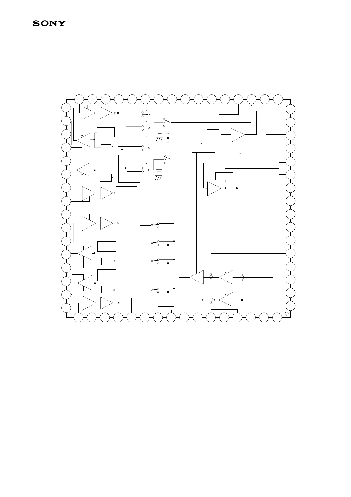
Block Diagram and Pin Configuration
CXA1702AR
REC1AOUT
REC1ACNT
V
CC1CH
REC1BCNT
REC1BOUT
PB1BIN
GND1B
PBDUMP1B
PBDUMP2A
GND2A
PB2AIN
REC2AOUT
REC2ACNT
V
CC2CH
REC2BCNT
REC2BOUT
Ø
CC
PBDUMP1A
PB1AIN
GND1A
MTQ
REC1A
RAMP
V
REC2A
REC1B
REC2B
XHRFSWP
MTF
RFSWP
PCMOUT
22 21 20 19 18 1723242526272829303132
33
HEAD
15dB
34
35
40dB
REC 1A
REC
RAMP
GEN
36
37
REC
RAMP
GEN
38
REC 1B
HEAD
40dB
15dB
39
PCMSW1
V/I
V/I
PCMSW2
VIDEOSW1
VIDEOSW2
1A
1B
1A
1B
2A
2B
2A
2B
PCMSW3 (6dB)
1CH
2CH
MUTE
GND
1CH
2CH
MUTE
VIDEOSW3 (0dB)
GND
MT (-6dB)
RF
AGC
12dB
DOCDE T
AG CDE T
40
41
VIDEO
HEAD
42
43
REC 2A
REC
44
45
46
REC
REC 2B
47
HEAD
40dB
40dB
15dB
RAMP
GEN
V/I
RAMP
GEN
V/I
15dB
VPSW1
VPSW2
VPSW3
VPSW4
PCM
VIDEO
PCM
VIDEO
PCM
VIDEO
PCM
YGCA
1
LOW
GCA
1
1
LOW
GCA
2
1
1
1
48
49 50 51 52 53 54 55 56 57 58 59 60 61 62 63 64
BUFF
2
CC
V
MTOUT
RP_PB
16
DOP
15
DOCDET
14
RFAGCIN
13
RFAGCTC
12
RFAGCOUT
11
REFV
10
T2
9
YLEV
_MTG
8
T1
7
LOWLEVEL
6
YIN
5
XDECK
4
CIN
3
GND2
2
AFMIN
1
IR
IR1
GND2B
PB2BIN
VREG
RECPCM
PBDUMP2B
VPPCMIN
VPVTRIN
GND
RECVTR
VG2
PCMIN
PCMREC
ATFIN
AFREC
—2—
CXA1702AR
Pin Description (VCC, VCC2, VCC1CH, VCC2CH=4.75V, Ta=25°C)
Pin
Pin voltage
Symbol
No. DC AC
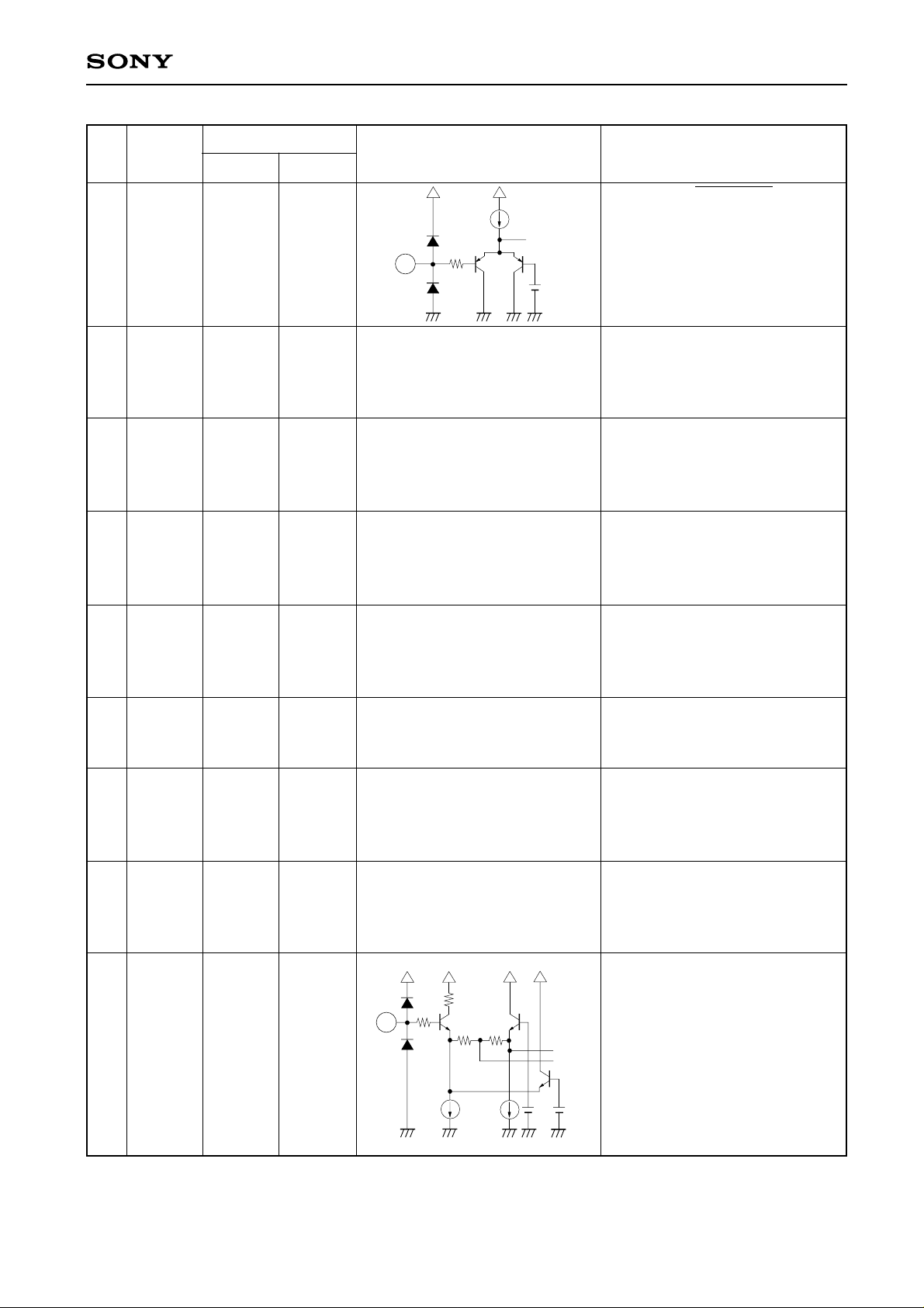
1 AFM IN — 125mVp-p
input
2 GND2 0V —
3 CIN 2.45V 500mVp-p
input
4 XDECK 2.4V —
(when pin
is open)
H: 4.3 V
or more
L: 0.6 V
or less
input
5 YIN 2.45V 500mVp-p
input
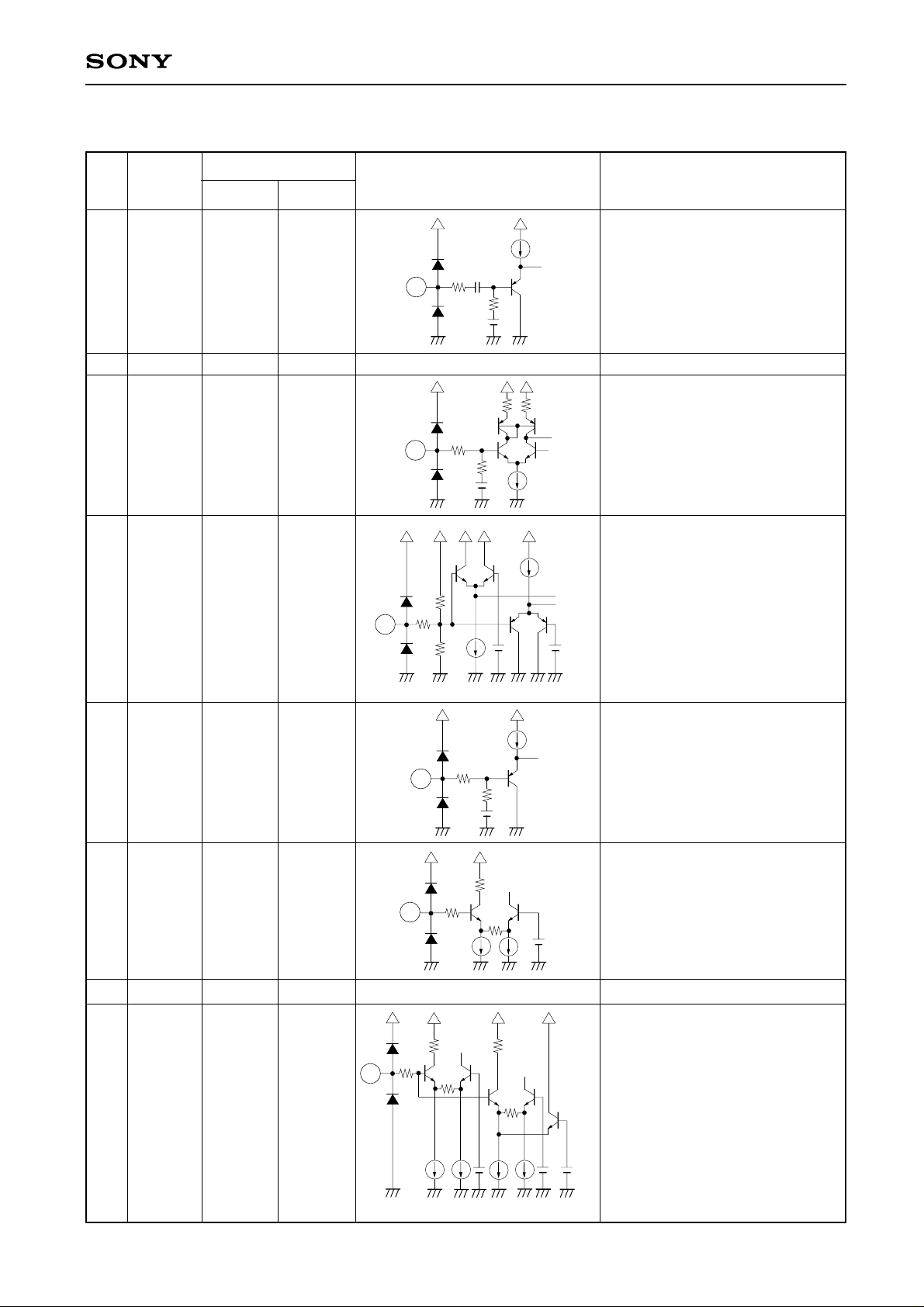
Equivalent circuit Description
Input pin for recording AFM
70µ
140
20p
50k
2.45V
1
signal. Input signal bias should
be in the range from 1 V to 3.5 V.
Connect to Vcc when the pin is
not in use.
GND pin
Input pin for recording chroma
signal.
3
140
50k
2.45V
25µ
DECK and NORM switching pin
20µ
100k
4
140
100k
20µ
2.9V
1.8V
H : NORM (4ch)
L:
Open :
DECK (2ch)
}
Input pin for recording Y signal.
40µ
6 LOW 1.8V to —
LEVEL 4.75V
input
7T1 — —
8
YLEV_MTG
1.8V to —
4.75V
input
5
140
50k
2.45V
EVR adjusting pin for low-band
270
6
140
90µ
21k
3.15V
90µ
—
recording signal (chroma, AFM,
video path ATF, PCM path ATF)
level. Increasing the input
voltage lowers the signal level.
Test pin. Set the pin open.
EVR adjusting pin for recording Y
270
8
140
23k
270
14k
signal level and middle tune boost
amount. Adjusts the former during
recording and the latter during
playback. Increasing the input
voltage lowers recording Y signal
90µ
90µ
3.2V
YLEVEL MTG
100µ100µ
2.8V
level and boost amount.
1.75V
—3—
CXA1702AR
Pin
Pin voltage
Symbol
No. DC AC
9T2 — —
10 REFV Hi8:4.45V
Nor:3.6V
input
11 RFAGC 1.9V 400mVp-p
OUT output
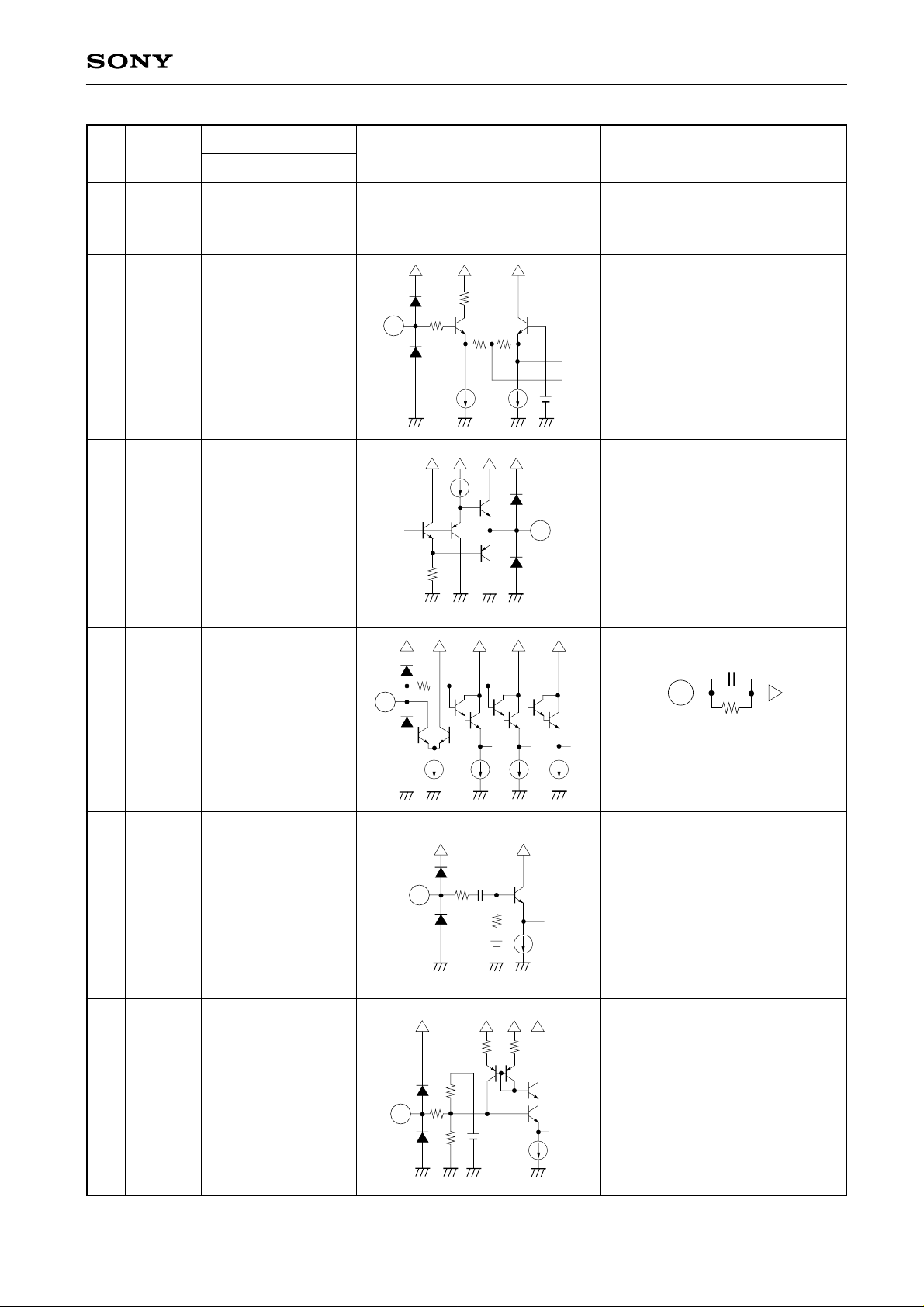
Equivalent circuit Description
Test pin. Connect decoupling
capacitance between this pin and
GND.
EVR adjusting pin to decide the
270
10
140
60k
15k
adjustment range of middle tune
fo.
Input the following:
Hi8: 4.45 V
Nor: 3.6 V
40µ
40µ
3.25V
Output pin for playback Y signal.
40µ
11
2k
12 RFAGCTC 2.5V to —
4.75V
input
(during
EVR adjustment)
13 RFAGC — 220mVp-p
IN input
14 DOCDET 2.55V —
(when pin
is open)
600µ
410µ
RFAGC time constant pin.
12
4700p
470k
V
CC
140
12
RFAGCTC
RFAGC gain may be adjusted by
50µ
50µ
25µ 25µ
EVR. Increasing the input
voltage increases gain.
Input pin for playback Y signal.
Playback Y signal is separated
from playback video signal output
to Pin 17 (MTOUT), then input to
Pin 13 (RFAGCIN). Set input
signal bias in the range from 1 V
140
13p
50k
3.25V
50µ
13
to 3.5 V. Connect to Vcc when
this pin is not in use.
Pin for deciding dropout detection
level. Connect decoupling
capacitance between this pin and
26.5k
14
140
42.5k
4.15V
50µ
GND. For adjustment, input
voltage proportional to Pin 52
(VREG) output voltage.
Increasing the input voltage
increases the detection level.
—4—
CXA1702AR
Pin
Pin voltage
Symbol
No. DC AC
15 DOP H: 3.15V —
L: 0V
output
16 RP_PB H: 2.3V —
or more
L: 0.6V
or less
input
17 MTOUT 2.4V 220mVp-p
(playback
Y signal)
output
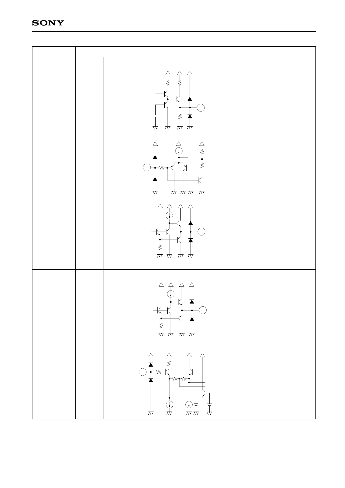
Equivalent circuit Description
Output pin for dropout detection
150
signal. Goes High at the time of
dropout.
35µ
2.15V
15
Input pin for REC/PB switching
50k
5.4k
signal.
H : PB
L : REC
3.15V
2.4k
1.3m
16
140
Output pin for playback video
40µ
17
signal.
18 Vcc2 4.75V —
19 PCMOUT 1.95V 220mVp-p
output
20 MTF0 1.8V to —
4.75V
input
4k
400µ
330µ
Power supply pin.
Output pin for playback PCM
3.5k
360µ
25µ
19
240µ
signal.
EVR adjusting pin for middle tune
270
20
140
40µ
30k
40µ
11k
2.85V
fo. Increasing the input voltage
increases fo.
1.7V
—5—
CXA1702AR
Pin
Symbol
Pin voltage
Equivalent circuit Description
No. DC AC
21 XHRFSWP H: 2.3V —
or more
L: 0.6V or
less input
21
140
22 RFSWP H: 2.3V — Same as for Pin 21
or more
L: 0.6V or
less input
23 REC2B H: 2.3V — Same as for Pin 21
or more
L: 0.6V or
less input
24 REC2A H: 2.3V — Same as for Pin 21
or more
L: 0.6V or
less input
25 REC1B H: 2.3V — Same as for Pin 21
or more
L: 0.6V or
less input
26 VCC 4.75V — —
27 REC1A H: 2.3V — Same as for Pin 21
or more
L: 0.6V or
less input
28 RAMP H: 2.3V — Same as for Pin 21
or more
L: 0.6V or
less input
29 MTQ 1.8V to —
4.75V
input
29
140
270
37.5k
12.5k
35µ
Input pin for 1/2RFSWP signal.
2.15V
Input pin for RFSWP signal.
Goes L during recording and
turns on 2Bch recording amplifier
output bias current.
Goes L during recording and
turns on 2Ach recording amplifier
output bias current.
Goes L during recording and
turns on 1Bch recording amplifier
output bias current.
Power supply pin for main blocks
excluding recording and head
amplifiers.
Goes L during recording and
turns on 1Ach recording amplifier
output bias current.
Goes H during after-recording
and turns on recording amplifier
output bias current.
EVR adjusting pin for middle tune
Q. Increasing the input voltage
increases Q.
40µ
—6—
40µ
2.9V
1.8V
CXA1702AR
Pin
Symbol
Pin voltage
Equivalent circuit Description
No. DC AC
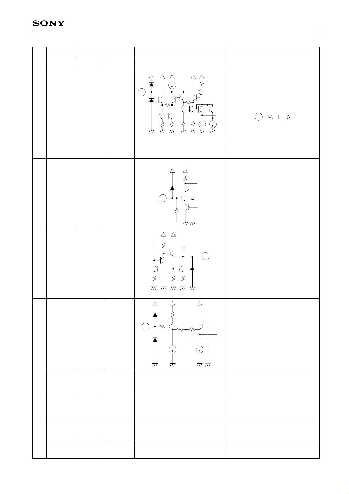
30 PBDUMP1A 2.6V —
120µ
30
31 GND1A 0V — —
32 PB1AIN 0.7V 200µVp-p
input
32
1.2m
1.5V
270
130µ
Dumping adjusting pin for 1Ach
head amplifier. Increasing the
external resistance reduces the
peaking amount.
40µ
30
PBDUMP1A
GND pin for 1Ach recording and
head amplifiers.
Playback signal 1Ach input pin.
33 REC1A (19mA (21mAp-p
OUT output) output)
19m
34 REC1A 1.8V to —
CNT 4.75V
270
input
34
140
52K
40µ
35 Vcc1CH 4.75V — —
36 REC1B 1.8V to — Same as for Pin 34.
CNT 4.75V
input
37 REC1B (19mA (21mAp-p Same as for Pin 33.
OUT output) output)
38 PB1BIN 0.7V 200µVp-p Same as for Pin 32.
input
19K
40µ
Recording signal 1Ach output pin.
Open collector.
33
EVR adjusting pin for 1Ach
recording amplifier dumping.
Increasing the input voltage
increases the peaking amount.
3.15V
Power supply pin for 1Ach and
1Bch recording and head
amplifiers.
EVR adjusting pin for 1Bch
recording amplifier dumping.
Recording signal 1Bch output pin.
Open collector.
Playback signal 1Bch input pin.
—7—
CXA1702AR
Pin
Symbol
Pin voltage
Equivalent circuit Description
No. DC AC
39 GND1B 0V — —
40 PBDUMP1B 2.6V — Same as for Pin 30.
41 PBDUMP2A 2.6V — Same as for Pin 30.
42 GND2A 0V — —
43 PB2AIN 0.7V 200µVp-p Same as for Pin 32.
input
44 REC2AOUT (19mA (21mAp-p Same as for Pin 33.
output) output)
GND pin for 1Bch recording and
head amplifiers.
Dumping adjusting pin for 1Bch
head amplifier.
Dumping adjusting pin for 2Ach
head amplifier.
GND pin for 2Ach recording and
head amplifiers.
Playback signal 2Ach input pin.
Recording signal 2Ach output pin.
Open collector.
45 REC2ACNT 1.8V to — Same as for Pin 34.
4.75V
input
46 VCC2CH 4.75V — —
47 REC2BCNT 1.8V to Same as for Pin 34.
4.75V
input
48 REC2BOUT (19mA (21mAp-p Same as for Pin 33.
output) output)
49 PB2BIN 0.7V 200µVp-p Same as for Pin 32.
input
50 GND2B 0V — —
51 PBDUMP2B 2.6V — Same as for Pin 30.
EVR adjusting pin for 2Ach
recording amplifier dumping.
Power supply pin for 2Ach and
2Bch recording and head
amplifiers.
EVR adjusting pin for 2Bch
recording amplifier dumping.
Recording signal 2Bch output pin.
Open collector.
Playback signal 2Bch input pin.
GND pin for 2Bch recording and
head amplifiers.
Dumping adjusting pin for 2Bch
head amplifier.
—8—
 Loading...