

Sony CXA1685M Datasheet
High-Speed Transimpedance Amplifier
Description
CXA1685M is a low noise transimpedance
amplifier, particularly suitable for fiber-optic system.
CXA1685M is fabricated using high-speed bipolar
process.
Features
• High transimpedance: Q 11.2kΩ (Typ.)
Q 10.8kΩ (Typ.)
• Wide band width (–3dB): Q 177MHz (Typ.)
Q 157MHz (Typ.)
• Maximum input current: 1mA
• Low noise: 1.7pA/√ Hz (Typ.)
Applications
• SONET/SDH: 155Mb/s
• Fiber channel:133Mb/s
• FDDI: 125Mb/s
Absolute Maximum Ratings
• Supply voltage VCC – VEE –0.3 to +7.0 V
• Minimum input voltage VIN VEE V
• Input current IIN –1 to +1 mA
• Output current
(Q/Q) (Continuous) IO 0 to 50 mA
(Surge) 0 to 100 mA
• Storage temperature Tstg –65 to +150 °C
Recommended Operating Conditions
• DC power supply voltage
VCC – VEE 4.75 to 5.46 V
• Operating ambient temperature
Ta 0 to +85 °C
Structure
Bipolar silicon monolithic IC
– 1 –
E94X22A8Y
Sony reserves the right to change products and specifications without prior notice. This information does not convey any license by
any implication or otherwise under any patents or other right. Application circuits shown, if any, are typical examples illustrating the
operation of the devices. Sony cannot assume responsibility for any problems arising out of the use of these circuits.
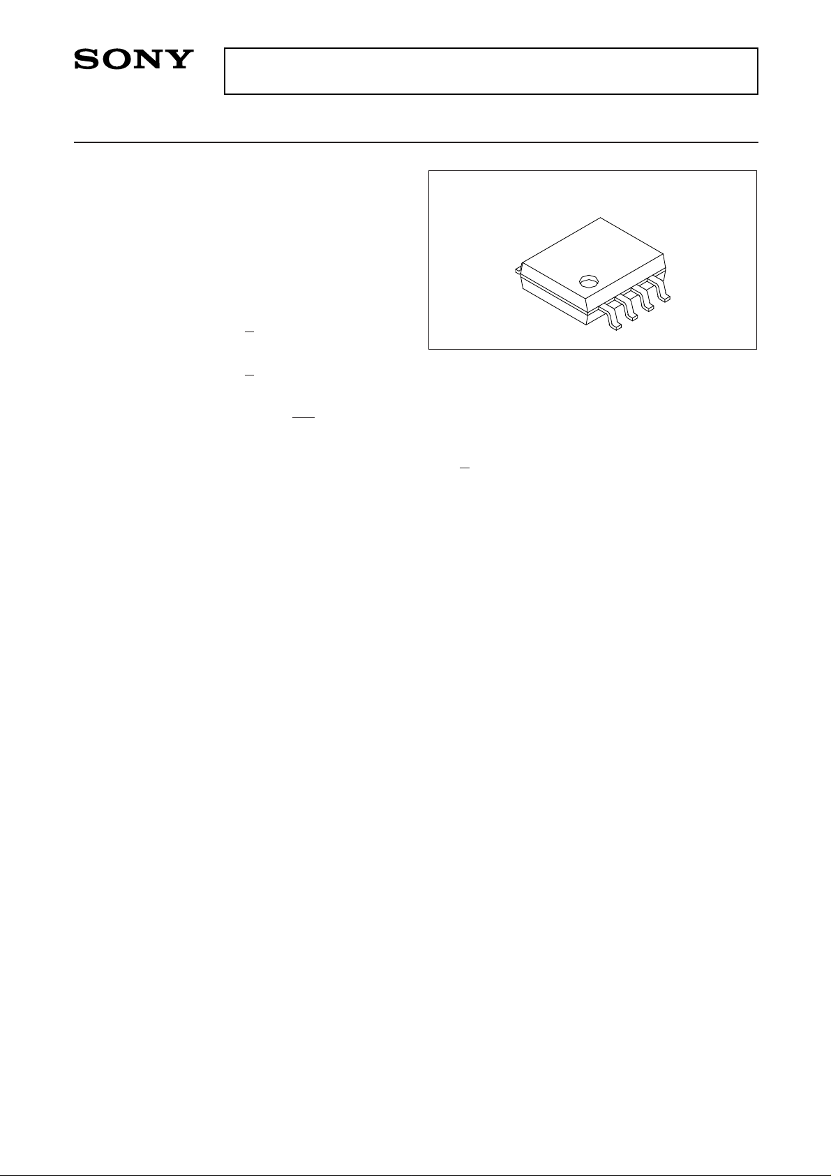
CXA1685M
8 pin SOP (Plastic)
– 2 –
CXA1685M
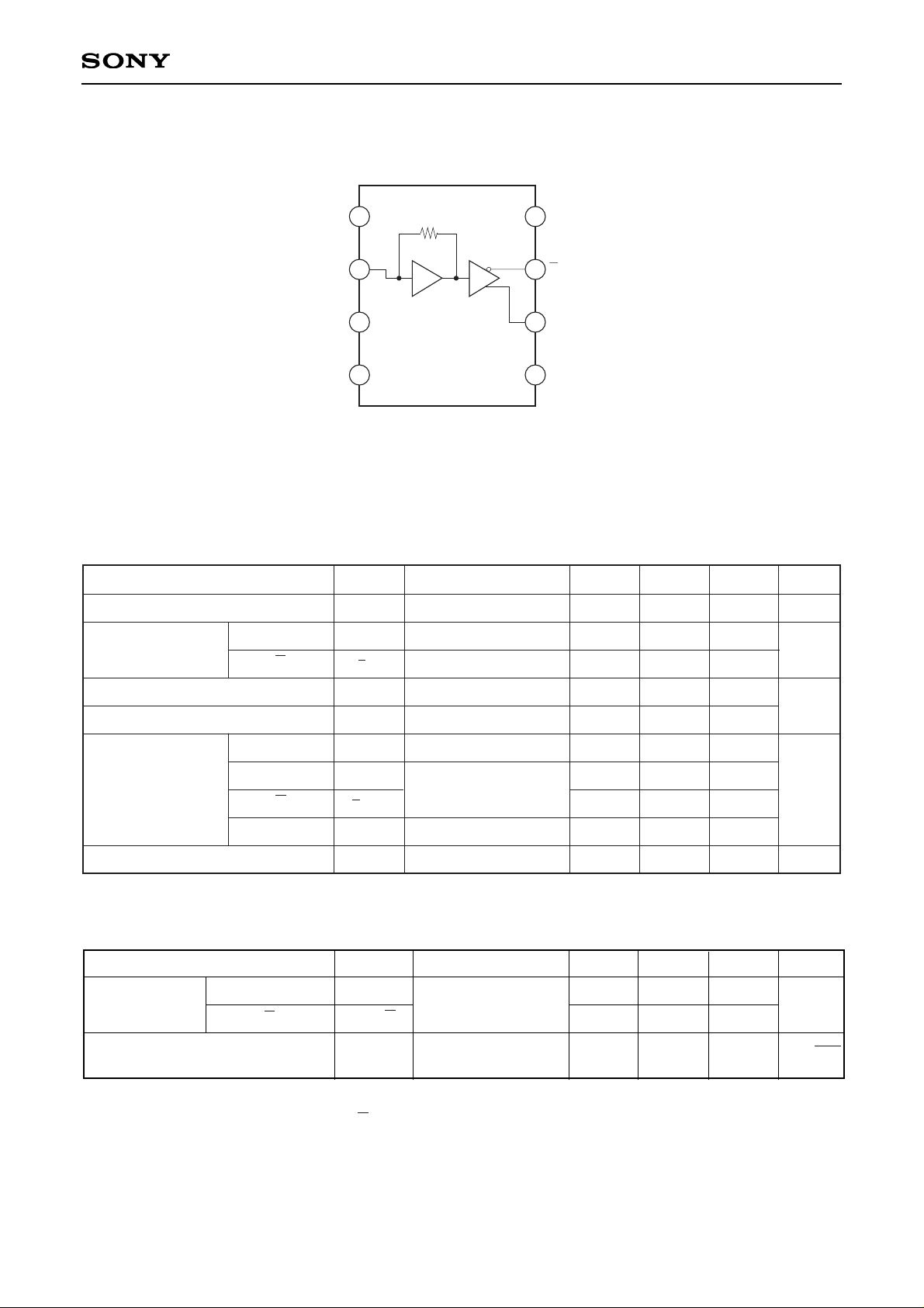
Block Diagram and Pin Assignment
• AC Electrical Characteristics (VCC = VCCA = GND, VEES = VEEDA = –5.46 to –4.75V, Ta = 0 to +85°C)
Item
Symbol
Test Condition
Min.
Typ.
Max. Unit.
Bandwidth
(–3dB)
Input Current Noise Spectral
Density (Mean value)
Q
Q
f–3dBQ
f–3dBQ
∗1
In
fN = 1kHZ to 156MHZ
113
109
177
157
1.7
MHZ
pA/√ HZ
∗1
Assumes photodiode capacitance; CPD < 1.0pF, output load capacitance; Cout = 2.0pF,
output load resistor; Q: 620Ω to VEE, Q: 1.3kΩ to VEE
4
5
7
8
1
2
3
6
ZT
VCCAVCC
Q
IN
QC
V
EEDAVEES
Electrical Characteristics
• DC Electrical Characteristics (VCC = VCCA = GND, VEES = VEEDA = –5.46 to –4.75V, Ta = 0 to +85°C)
Item Symbol
Test Condition
Min.
Max.
Typ.
Unit
Supply current
Transimpedance
Max. Input Current before clipping
Max. Input Current
Bias votlage
IEE
ZTQ
ZTQ
IIN
IIN2
VIN
VQ
VQ
VC
CIN
input pin left open
Q
Q
IN
Q
Q
C
input pin left open
–15.3
6.6
6.2
+40
+1000
–10.0
11.2
10.8
VEE + 2.5
VEE + 1.7
VCC – 2.4
VEE + 1.7
1.3
14.8
14.3
Ta = 25°C
Input capacitance
mA
kΩ
µA
V
pF
– 3 –
CXA1685M
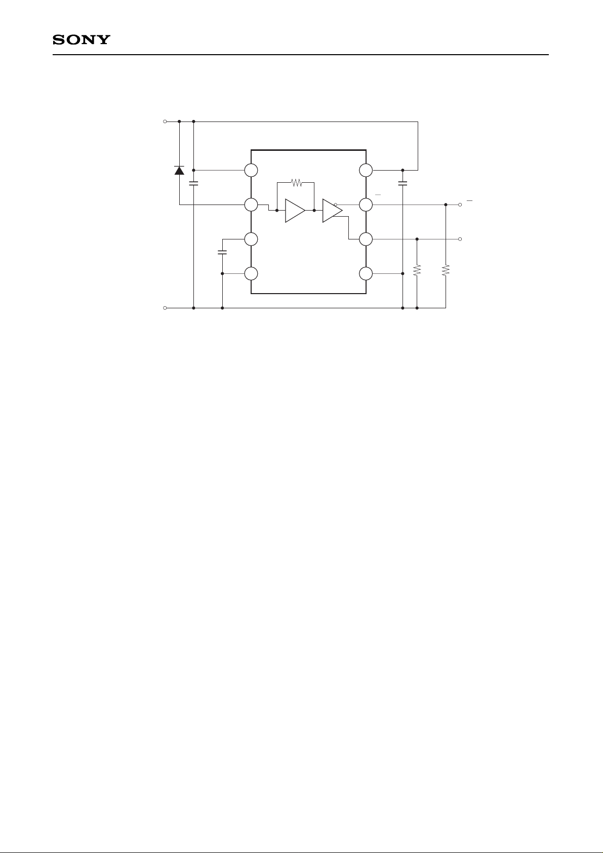
Application Circuit
Application circuits shown are typical examples illustrating the operation of the devices. Sony cannot assume responsibility for
any problems arising out of the use of these circuits or for any infringement of third party patent and other right due to same.
Cautions for Handling
1. As the electronic breakdown level is weak, take care to handle.
2. The internal resistor of the output pin does not have the capability of drive (RL = 10kΩ). The terminal
resistors must be connected. The resistance value is shown in application circuit.
VCCAVCC
IN
QC
V
EEDAVEES
4
5
7
8
1
2
3
6
ZT
Q
V
CC
VEE
1.0µF
0.1µF
0.1µF
620Ω 1.3kΩ
PD
Q
Q
 Loading...