

Sony CXA1645P, CXA1645M Datasheet
RGB Encoder
For the availability of this product, please contact the sales office.
Description
The CXA1645P/M is an encoder IC that converts
analog RGB signals to a composite video signal. This
IC has various pulse generators necessary for
encoding. Composite video outputs and Y/C outputs for
the S terminal are obtained just by inputting composite
sync, subcarrier and analog RGB signals.
It is best suited to image processing of personal
computers and video games.
Features
• Single 5V power supply
• Compatible with both NTSC and PAL systems
• Built-in 75Ω drivers
(RGB output, composite video output, Y output, C
output)
• Both sine wave and pulse can be input as a
subcarrier.
• Built-in band pass filter for the C signal and delay
line for the Y signal
• Built-in R-Y and B-Y modulator circuits
• Built-in PAL alternate circuit
• Burst flag generator circuit
• Half H killer circuit
CXA1645P/M
24 pin DIP (Plastic)
Structure
Bipolar silicon monolithic IC
Absolute Maximum Ratings
• Supply voltage VCC 14 V
• Operating temperature Topr –20 to +75 °C
• Storage temperature Tstg –65 to +150 °C
• Allowable power PD CXA1645P 1250 mW
dissipation CXA1645M 780 mW
Recommended Operating Condition
Supply voltage VCC1, 2 5.0 ± 0.25 V
24 pin SOP (Plastic)
Applications
Image processing of video games and personal
computers
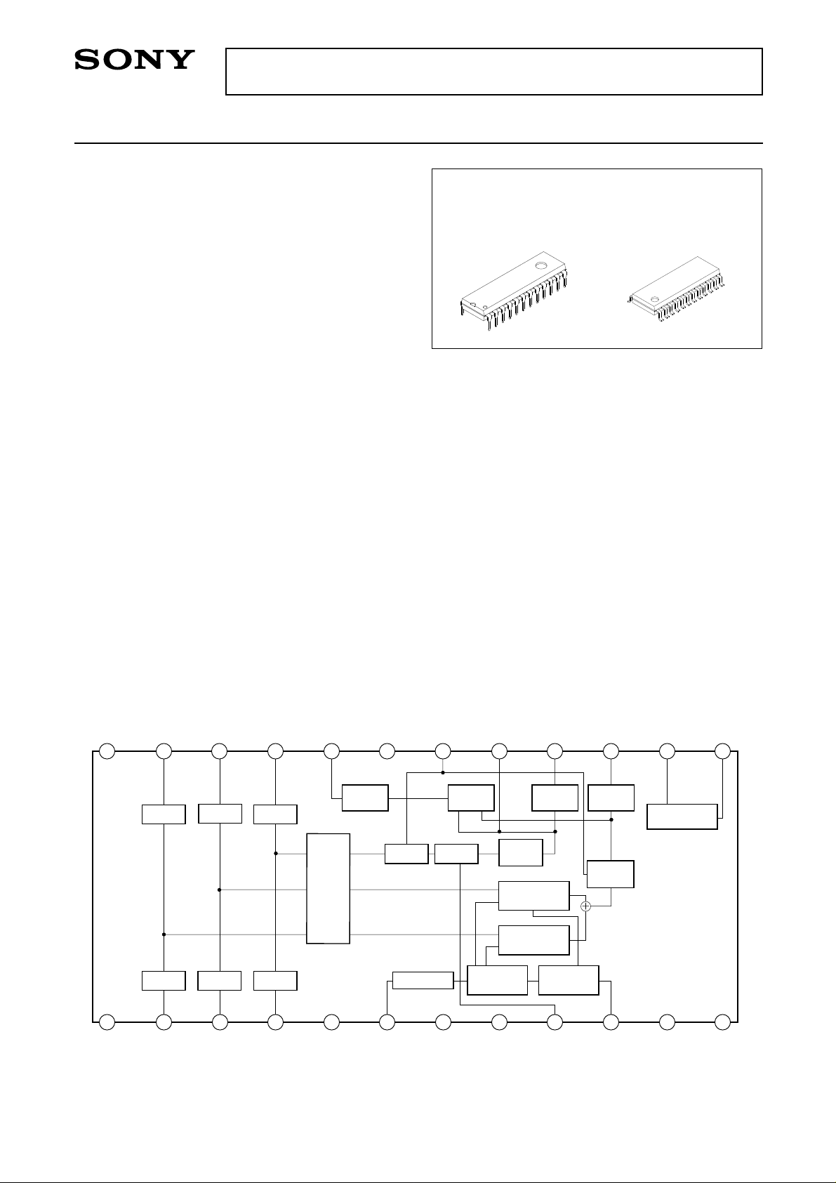
Block Diagram and Pin Configuration
24
1
23
R-OUT
CLAMP CLAMP CLAMP
2
22
G-OUT
3
21
B-OUT
4
20
MATRIX
5
VIDEO
OUT
CC2BOUTGOUTROUTGND2 VREF IREFCVOUT
19
DELAY
SIN-PULSE
6
18
CLAMP
7
Y/C
MIX
SHIFTER
17
PHASE
8
16
75
DRIVER75DRIVER
SYNC
ADD
R-Y
Modulator
B-Y
Modulator
PULSE
9
COUTYOUTYTRAPFOV
15
BPF
GEN
10
SYNCINYCLPCBFOUTNPINSCINBINGINRINGND1 NC V
14
REGULATOR
11
13
12
CC1NC
Sony reserves the right to change products and specifications without prior notice. This information does not convey any license by
any implication or otherwise under any patents or other right. Application circuits shown, if any, are typical examples illustrating the
operation of the devices. Sony cannot assume responsibility for any problems arising out of the use of these circuits.
– 1 –
E93411A41-ST
CXA1645P/M
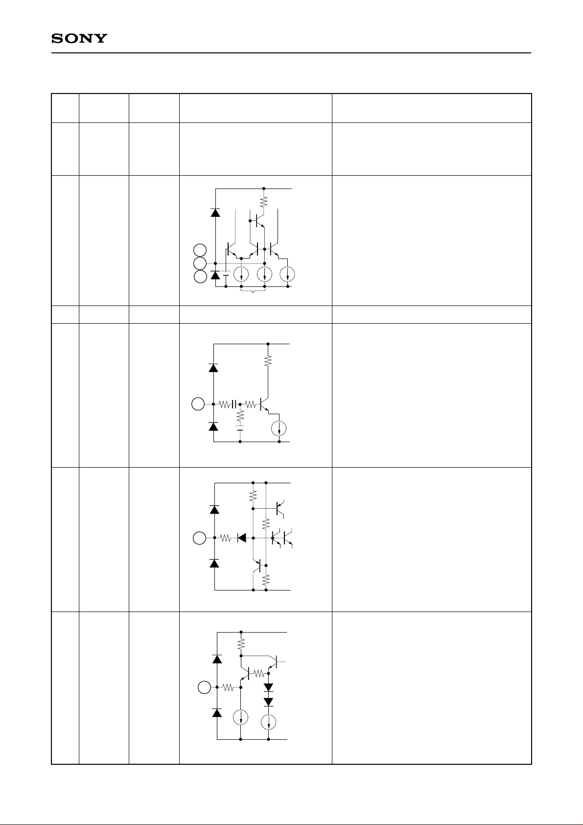
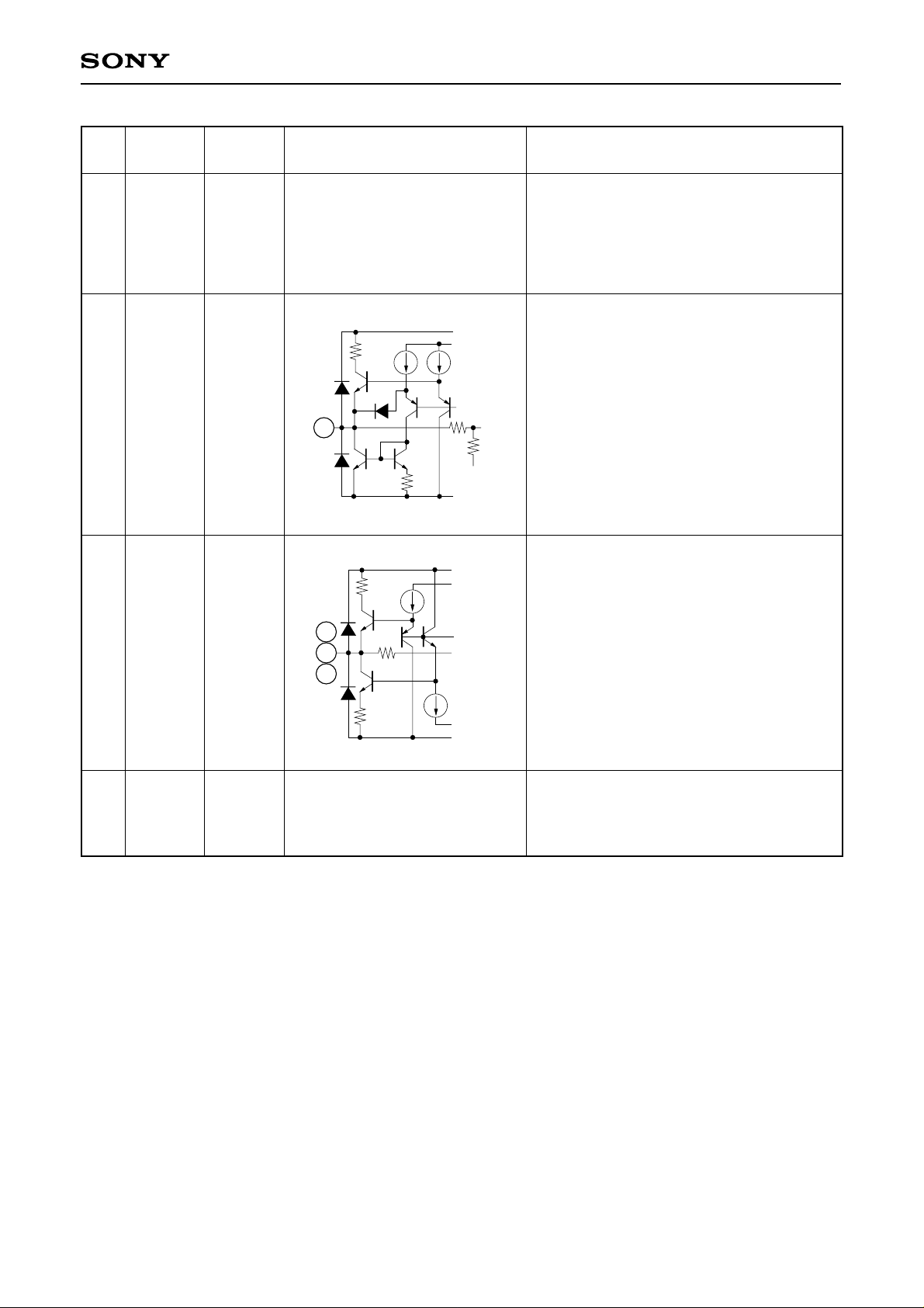
Pin Description
Pin
No.
Symbol Pin voltage
1
GND1
RIN
2
GIN
3
BIN
4
NC
5
∗
0V
Black level
when
clamped
2.0V
Equivalent circuit Description
Ground for all circuits other than RGB,
composite video and Y/C output circuits.
The leads to GND2 should be as short and
wide as possible.
VCC1
Analog RGB signal inputs. Input
100%, = 1Vp-p (max.). To minimize clamp
error, input at as low impedance as
2
3
4
100µ
ICLP
180µ
100µ
GND1
possible.
ICLP turns ON only in the burst flag period.
NO CONNECTION
V
CC1
∗
Externally applied voltage
Subcarrier input.
SCIN
6
NPIN
7
—
1.7V
20k
129
3k
20P
80k
20k
2.5V
68k
32k
100µ
GND1
CC1
V
GND1
CC1
V
6
7
Input 0.4 to 0.5Vp-p sine wave or pulse.
Refer to Notes on Operation, Nos. 3 and 5.
Pin for switching between NTSC and PAL
modes
NTSC: VCC, PAL: GND
8
BFOUT
H : 3.6V
L : 3.2V
8
129
25µ
25µ
GND1
BF pulse monitoring output. Incapable of
driving a 75Ω load.
– 2 –
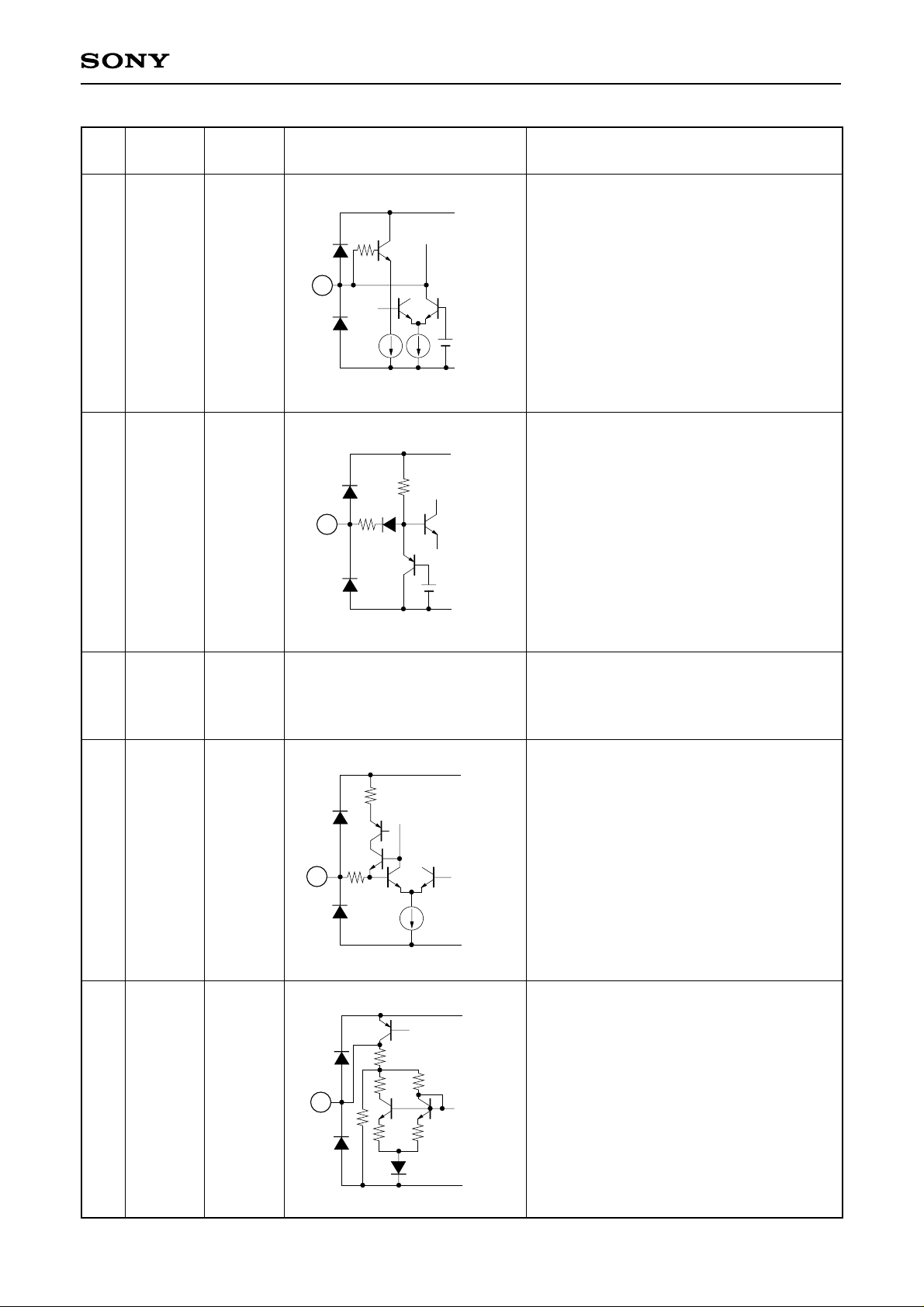
CXA1645P/M
Pin
No.
9
10
Symbol Pin voltage
YCLPC
SYNC
IN
2.5V
2.2V
Equivalent circuit Description
V
CC1
129
9
Pin to determine the Y signal clamp time
constant.
Connect to GND via a 0.1µF capacitor.
40k
1.6V
GND1
CC1
V
5µ
Composite sync signal input. Input TTL-
10
4k
level voltages.
L ( ≤ 0.8V): SYNC period
H ( ≥ 2.0V)
2.2V
GND1
12
13
14
VCC1
IREF
VREF
5.0V
2.0V
4.0V
∗
composite video and Y/C output circuits.
Refer to Notes on Operation. Nos. 4 and 10.
Power supply for all circuits other than RGB,
V
CC1
Pin to determine the internal reference
current.
13
129
50µ
GND1
V
CC1
Connect to GND via a 47kΩ resistor.
Internal reference voltage.
Connect a decoupling capacitor of
14
approximately 10µF.
GND1
– 3 –
Refer to Notes on Operation, Nos. 4 and 7.
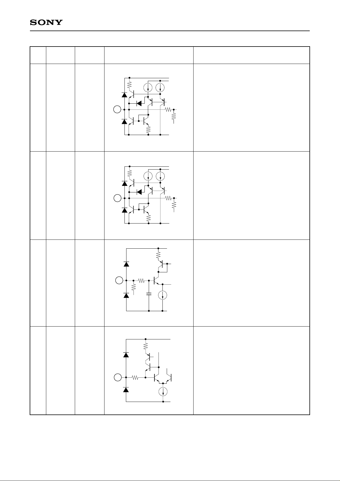
CXA1645P/M
Pin
No.
15
16
Symbol Pin voltage
COUT
YOUT
2.2V
Black level
1.3V
Equivalent circuit Description
V
CC2
CC1
V
600µ
Chroma signal output. Capable of driving a
75Ω load.
15
20k
GND2
V
V
600µ
CC2
CC1
Refer to Notes on Operation, Nos. 6 and 9.
10k
Y signal output. Capable of driving a 75Ω
load.
16
20k
Refer to Notes on Operation, Nos. 6 and 9.
10k
17
18
YTRAP
FO
Black level
1.6V
2.0V
17
8.5k
1.5k
Input resistance 1.5kΩ
18
129
0.5P
GND2
V
CC1
GND1
V
CC1
50µ
Pin for reducing cross color caused by the
subcarrier frequency component of the Y
signal. When the CVOUT pin is in use,
connect a capacitor or a capacitor and an
inductor in series between YTRAP and
GND. Decide capacitance and inductance,
giving consideration to cross color and the
required resolution.
No influence on the YOUT pin.
Refer to Notes on Operation, No. 8.
Internal filter fo adjustment pin.
Connect to GND via the following resistor
according to the NTSC or PAL mode.
NTSC: 20kΩ (±1%)
PAL : 16kΩ (±1%)
GND1
– 4 –
CXA1645P/M
Pin
No.
19
20
Symbol Pin voltage
VCC2
CVOUT
Black level
5.0V
1.2V
∗
Equivalent circuit Description
Power supply for RGB, composite video and
Y/C output circuits. Decouple this pin with a
large capacitor of 10µF or above as a high
current flows.
Refer to Notes on Operation, Nos. 4 and 10.
VCC2
V
CC1
600µ
Composite video signal output. Capable of
driving a 75Ω load.
20
500µ
20k
GND2
CC2
V
V
CC1
Refer to Notes on Operation, Nos. 6 and 9.
10k
21
22
23
24
BOUT
GOUT
ROUT
GND2
Black level
1.7V
∗
0V
21
22
23
Analog RGB signal outputs. Capable of
driving a 75Ω load.
5.5k
Refer to Notes on Operation, Nos. 6 and 9.
200µ
GND1
GND2
Ground for RGB, composite video and Y/C
output circuits. The leads to GND1 should
be as short and wide as possible.
– 5 –
 Loading...