

Sony CXA1599Q Datasheet

1-chip Cassette Deck
For the availability of this product, please contact the sales office.
Description
The CXA1599Q is an IC for audio cassette decks.
All analog signal processing functions, except Dolby
NR, are incorporated in a single chip. As a result, a
double cassette deck system can be simply
configured by adding a Dolby IC.
Features
• Electronic recording volume for setting recording
level (with a balance volume)
• Recording equalizer amplifier
(with calibration and low frequency boost
functions)
• Recording mute function
(soft mute and fader possible)
• Playback head amplifier switch function
(deck A/B switch)
• NR pass amplifier (NR IN/PASS switch)
• Headphone amplifier with electronic volume
• Full-wave rectifier output amplifier for level meter
(with time constant function)
• HPF amplifier for AMS
(with BS/AMS gain switch function)
• Electronic switch for tape EQ selection
(120µs/70µs)
• Electronic switch for metal tape selection
• Electronic switch for normal/double speed dubbing
selection (only for recording equalizer)
• Line mute function
• Double cassette dubbing system can be easily
configured with this single IC.
CXA1599Q
48 pin QFP (Plastic)
Applications
Analog signal processing (except Dolby NR) for
stereo analog cassette deck
(ALPS ELECTRIC CO., LTD. HADKH-55460 head
applicable)
Structure
Bipolar silicon monolithic IC
Absolute Maximum Ratings (Ta = 25°C)
• Supply voltage VCC 17 V
• Operating temperature Topr –20 to +75 °C
• Storage temperature Tstg –65 to +150 °C
• Allowable power dissipation PD 735 mW
Operating Conditions
Supply voltage VCC ±5.0 to ±8.0 V
(positive/negative dual power supply)
10.0 to 16.0 V
(single power supply)
Sony reserves the right to change products and specifications without prior notice. This information does not convey any license by
any implication or otherwise under any patents or other right. Application circuits shown, if any, are typical examples illustrating the
operation of the devices. Sony cannot assume responsibility for any problems arising out of the use of these circuits.
– 1 –
E92Y05-ST
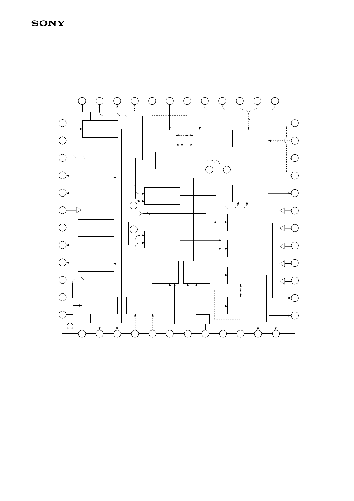
Block Diagram
BOOST2
36
LINE OUT2
35
LINE OUT1
34
REC VOL
33
REC BAL
32
LINE IN2
31
LINE IN1
30
DECK A/B
29
28
A EQ
AMS BS
27
LINE MUTE
26
CXA1599Q
NR PASS
25
REC IN2
NR IN2
PASS IN2
PB OUT2
VOL OUT2
GND (VG)
I REF
VOL OUT1
PB OUT1
PASS IN1
37
38
39
40
41
42
44
45
46
43
REC EQ
2
PB EQ
GND (VG)
BIAS
PB EQ
2
2
5
B EQ
24
REC VOLREC VOL
MODE
CONTROL
2
35
34
4
23
METAL
22
SPEED
21
REC MUTE
2
39
NR/PASS
2
AMS/BS
2
20
AMS OUT
19
DVccDGNDVccV
DVcc
METER
18
46
DGND
NR/PASS
17
16
15
Vcc
V
EE
PVEE
2
PB HEAD PB HEAD
METER
HEADPHONE
AMP
EE
EE
PV
NR IN1
REC IN1
47
48
REC EQ
BOOST1
2
REC OUT1
CALIBRATION
3
REC OUT2
REC
4
GP CAL
5
REC CAL
6
PB INB1
7
PB INB2
8
PB INA1
HEADPHONE
9
PB INA2
AMP
10
HP VOL
11
HP OUT1
Signal line
Control line
121
HP OUT2
14
13
METER2
METER1
– 2 –

CXA1599Q
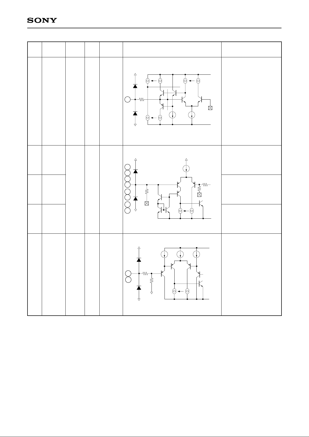
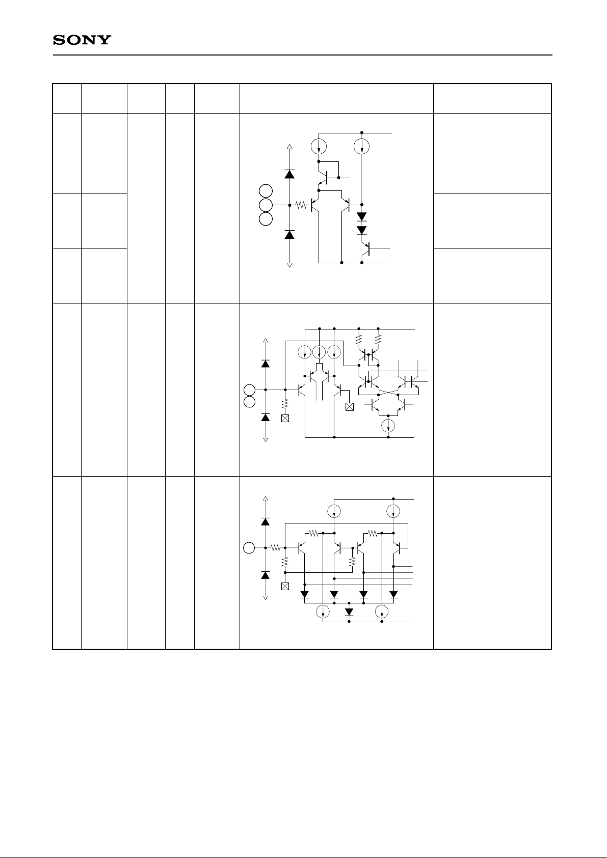
Pin Description (Ta = 25°C, Vcc = 7V, VEE = –7V, DVcc = 5V, No signal)
Pin
Symbol
No.
136BOOST1
BOOST2
23REC
OUT1
REC
OUT2
DC
voltage
I/O
resistance
0.0V — 9.5kΩ
0.0V O 0Ω
I/O
Equivalent circuit Description
Connects the external
capacitor for low
frequency boost of
recording equalizer
amplifier.
∗
When low frequency
boost is not executed:
During positive/
negative dual power
supply
→ Connect to GND.
During single power
supply
EE
→ Connect a
capacitor
36
VCC
VCC
× 2
500
4.8K
1
VEE
34k
VGS
5.5k
× 4
500
V
(over 3.3µF).
VCC
× 3
200
2
3
200
× 3
× 8
VCC
50k
5P
Output of recording
equalizer amplifier.
4
GP CAL
2.5V
(During
OPEN)
I 54kΩ
VEE
4
VCC
VEE
54k
VEE
DREF
VCC
VEE
Calibration for high
frequency gain of
recording equalizer
amplifier.
Controls by applying
the DC voltage of
DGND to DVcc.
High → Gain up
Low → Gain down
∗
When high frequency
calibration function is
not used, keep pin
open.
– 3 –
CXA1599Q
Pin
Symbol
No.
REC
5
CAL
6
PB INB1
7
PB INB2
8
PB INA1
9
PB INA2
3748REC IN2
REC IN1
3847NR IN2
NR IN1
DC
voltage
2.5V
(During
OPEN)
0.0V
I/O
I/O
resistance
I 54kΩ
50kΩ
I
Equivalent circuit Description
Calibration for overall
VCC
frequency gain of
VCC
recording equalizer
amplifier.
Controls by applying the
DC voltage of DGND to
5
54k
× 3
DREF
VEE
DVcc.
High → Gain up
Low → Gain down
∗
When recording
VEE
calibration function is
not used, keep this pin
open.
VCC
6
7
8
9
50k
37
48
38
47
VGS
VEE
VCC
VGS
Input of playback
equalizer amplifier.
Input of recording
equalizer amplifier.
Input pin for connecting
VEE
Dolby line (decode)
output signal.
10
33
HP
VOL
REC
VOL
0.0V
(During
OPEN)
I 100kΩ
VCC
Pin 10: Control for
CC
V
headphone volume
Pin 33: Control for
10
33
60k
40k
× 8
recording volume
Controls by applying
the DC voltage of
DGND to DVcc for
each pin.
DGND
VEE
High → Volume up
VEE
Low → Volume down
– 4 –
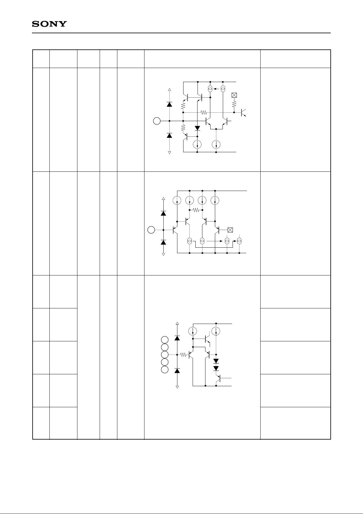
CXA1599Q
Pin
No.
11
12
Symbol
HP
OUT1
HP
OUT2
DC
voltage
I/O
resistance
0.0V O 0Ω
I/O
Equivalent circuit Description
VCC
10K
45k
5P
Output of headphone
volume
VEE
VCC
VCC
11
12
× 35
VEE
VCC
× 35
10P
× 4
× 11
× 4
× 7
1k
500
3k
1k
PVEE
METER1
13
14
15
16
METER2
PVEE
VEE
0.0V O —
–7.0V — —
17 Vcc 7.0V — —
18 DGND 0.0V — —
13
14
VEE
VCC
150
17
18
15
16
× 11
10k
To PVEE
To VEE
To VCC
To DGND
Output of level meter
amplifier
VEE
During positive/negative
dual power supply
→ Connect to negative
power supply.
During single power
supply
→ Connect to GND.
Positive power supply.
Connect to GND.
VCC
19 DVcc 5.0V — 60kΩ
15k
× 2
500
500
× 4
To each DREF
VEE
Power supply for
control.
19
30k
30k
DGND
VEE
– 5 –
CXA1599Q
Pin
No.
20
21
Symbol
AMS
OUT
REC
MUTE
DC
voltage
I/O
I/O
resistance
0.0V O 0Ω
—I —
21
20
VCC
VEE
Equivalent circuit Description
VCC
500
× 2
16k
VCC
VGS
4k
Output of AMS/BS
amplifier.
VEE
500
× 4
EE
V
Mute ON/OFF switch of
recording equalizer
VCC
amplifier.
Controls by applying the
DC voltage of DGND to
× 3
30k
× 3
DREF
DVcc.
High → Mute OFF
Low → Mute ON
∗
Soft mute/fader switch
is possible by changing
VEE
the time constant of the
external time constant
circuit.
22
23
26
27
29
SPEED
METAL
LINE
MUTE
AMS BS
DECK
A/B
—I —
23
26
27
29
22
VCC
VEE
10k
VCC
DGND
VEE
Tape speed switch
High → High speed
Low → Normal speed
Deck B metal tape
switch
High → Metal tape
Low → Norm, CrO2 tape
Line mute ON/OFF
switch
High → Mute OFF
Low → Mute ON
AMS/BS switch
High → AMS mode
Low → BS mode
Deck A/B playback
switch
High → PBINB
Low → PBINA
– 6 –
CXA1599Q
Pin
No.
24
25
28
30
31
Symbol
B EQ
NR
PASS
A EQ
LINE
IN1
LINE
IN2
DC
voltage
I/O
I/O
resistance
—I —
0.0V I 0Ω
Equivalent circuit Description
VCC
VCC
Deck B equalizer switch
High → 70µs EQ
(CrO2 tape)
Low → 120µs EQ
(Norm tape)
24
25
28
10k
NR/PASS input switch
High → PASS IN
Low → NR IN
DGND
VEE
VEE
Deck A equalizer switch
High → 70µs EQ
Low → 120µs EQ
× 2
VCC
Line input.
× 2
47kΩ resistance
connected externally.
VEE
VCC
30
31
5k
VGS
VEE
VGS
× 7
3k3k
× 7
× 2× 2
32
REC
BAL
2.5V
(During
OPEN)
VCC
VCC
Balance control of
70k
32
I
100kΩ
30k
11k
21K
11k
× 6× 6
recording volume
Controls by applying the
DC voltage of DGND to
DVcc.
High → VOL OUT1
DREF
VEE
Low → VOL OUT2
V
EE
– 7 –
 Loading...