

Sony CXA1598S, CXA1598M Datasheet

Description
The CXA1598M/S is a bipolar IC developed for
recording equalizer amplifier in analog cassette
decks. Incorporating the filter circuit has eliminated
the external inductor. Also, each of the six
parameters required for equalizer amplifiers can be
set independently with external resistance.
Features
• Inductor (coil) is unnecessary
• The six parameters (low frequency gain, medium
frequency gain, peaking gain, medium frequency
compensation frequency, peaking frequency, and
Q) required for recording equalizer amplifiers can
be set independently with external resistance
• Low frequency boost is possible with an external
capacitor
• Built-in recording mute function
(requiring only an external time constant circuit to
implement soft mute)
• Built-in 2 channels
• Small package
Applications
Recording equalizer amplifier for stereo analog
cassette decks
Structure
Bipolar silicon monolithic IC
Absolute Maximum Ratings
• Supply voltage VCC 17 V
• Operating temperature
Topr –20 to +75 °C
• Storage temperature
Tstg –65 to +150 °C
• Allowable power dissipation
PD (CXA1598M) 570 mW
(CXA1598S) 880 mW
Operating Conditions
Power supply Dual power supplies (VCC – VEE)
±6.5 to 8.0 V
Single power supply (VCC)
10.0 to 16.0 V
– 1 –
CXA1598M/S
E95131A8Y
Recording Equalizer Amplifier for Stereo Cassette Decks
Sony reserves the right to change products and specifications without prior notice. This information does not convey any license by
any implication or otherwise under any patents or other right. Application circuits shown, if any, are typical examples illustrating the
operation of the devices. Sony cannot assume responsibility for any problems arising out of the use of these circuits.
CXA1598M
24 pin SOP (Plastic)
CXA1598S
22 pin SDIP (Plastic)
– 2 –
CXA1598M/S
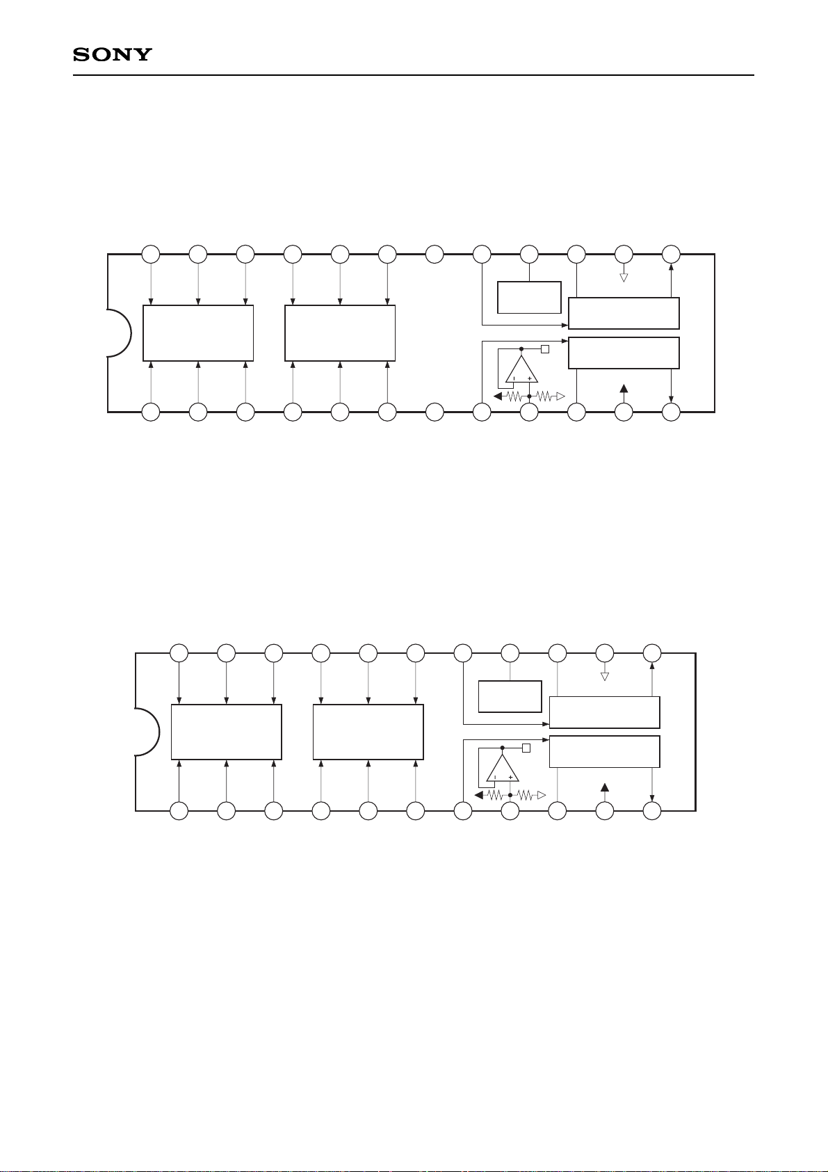
Block Diagram and Pin Configuration
CXA1598M
GND
BIAS
REC EQ
REC OUT1
BOOST1
V
EE
REC IN1
fM
DGND
f × Q
PARAMETER
CONTROL
REC EQ
V
CC
VEE
9
10
11
2
3
4
5
6
7
8
1
12
23
24
13
1415
16
17
18
19
20
21
22
VGS
FP CAL
REC MUTE
f/Q
IREF
REC OUT2
BOOST2
V
CC
REC IN2
GL
GH CAL
GP
GP CAL
REC CAL
GH
NC
NC
CXA1598S
GND
BIAS
REC EQ
REC OUT1
BOOST1
V
EE
REC IN1
fM
DGND
f × Q
PARAMETER CONTROL
REC EQ
V
CC
VEE
9
10
11
2
3
4
5
6
7
8
1
12
13
1415
16
17
18
19
20
21
22
VGS
FP CAL
REC MUTE
f/Q
IREF
REC OUT2
BOOST2
V
CC
REC IN2
GL
GH CAL
GP
GP CAL
REC CAL
GH
– 3 –
CXA1598M/S
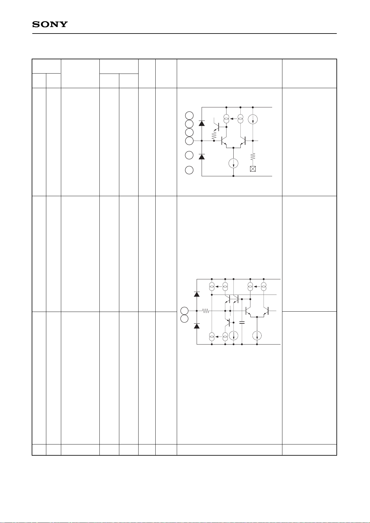
Pin Description (Ta = 25°C, VCC = 7.0V, VEE = –7.0V)
Pin No.
Symbol
I/O
Z (in) Equivalent circuit Description
Typical pin
voltage
DC AC
1
2
3
22
23
24
fxQ
f/Q
fM
GL
GH
GP
O —
Connection pins of
resistors for setting the
recording equalizer
amplifier parameters.
∗
Current input pins
used to set the
parameters for the
recording equalizer
amplifier.
∗
Setting currents for
each parameter are
generated by
attaching resistors
between these pins
and the DGND pin.
1.2V —
27k
DGND
192
2
3
22
23
24
1
(20)
(21)
(22)
CXA
1598M
CXA
1598S
1
2
3
20
21
22
4 FP CAL
I 54k
Peaking frequency
calibration pin.
∗
Controlled with DC
voltages of 0 to 5V.
High = Peaking
frequency
increased
Low = Peaking
frequency reduced
∗
Leave this pin
open when not
using the peaking
frequency
calibration function.
2.5V —
54k
4
19
(17)
4
19 REC CAL
I 54k
Recording level
calibration pin.
∗
Controlled with
DC voltages of 0
to 5V.
High = Recording
level gain
increased
Low = Recording
level gain reduced
∗
Leave this pin
open when not
using the
recording level
calibration
function.
Connected to GND.
2.5V —
17
5 DGND
I —
0.0V —
5
– 4 –
CXA1598M/S
6 REC MUTE
I —
Recording mute
ON/OFF selection pin.
∗
Recording mute is
controlled with DC
voltages of 0 to 5V.
High = Recording
mute OFF
Low = Recording
mute ON
∗
Soft mute and fader
can be switched
over by changing
the time constant of
the external time
constant circuit.
5.0V —
30k
6
6
8
17
REC IN1
REC IN2
I 50kΩ
Recording equalizer
amplifier input pin.
0.0V
–18dBv
GND
50k
8
17
(16)
(7)
7
16
10
15
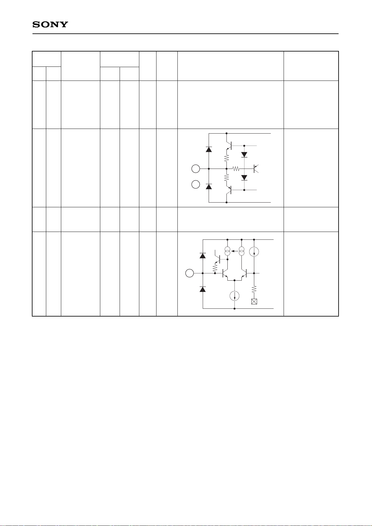
BOOST1
BOOST2
I 9.5kΩ
Connection pin of an
external capacitor for
low frequency boost.
∗
When low
frequency boost is
unnecessary,
connect to GND for
positive/negative
dual power
supplies; connect a
capacitor (3.3µF or
more) for a single
power supply.
0.0V —
4.8k 5.5k 35.5k
280
280
34k
GND
(9)
10
15
(14)
9
14
9 GND (VG)
I —
Connect to GND for
positive/negative
dual power supplies.
V
CC/2 (center
potential) for a single
power supply.
(Connect a capacitor
of 10µF or more)
0.0V
—
8
Pin No.
Symbol
I/O
Z (in) Equivalent circuit Description
Typical pin
voltage
DC AC
CXA
1598M
CXA
1598S
– 5 –
CXA1598M/S
11 VEE
I
—
Connect to the
negative power supply
for positive/negative
dual power supplies.
Connect to GND for a
single power supply.
–7.0V —10
12
13
REC OUT1
REC OUT2
O
—
Recording equalizer
amplifier output pin.
0.0V
–3.0dBv
11
12
14 VCC I —
Positive power
supply connection
pin.
7.0V —13
50k
200
200
12
13
(11)
(12)
16 IREF
O
—
Reference current
setting pin for
monolithic filter.
∗
The reference
current can be set
by attaching a
resistor between
this pin and
DGND.
1.2V —
15
(15)
16
27k
DGND
192
Pin No.
Symbol
I/O
Z (in) Equivalent circuit Description
Typical pin
voltage
DC AC
CXA
1598M
CXA
1598S

– 6 –
CXA1598M/S
20 GH CAL
I —
Medium frequency
calibration pin.
∗
Controlled with
DC voltages of 0
to 5V.
High = Medium
frequency level
gain increased
Low = Medium
frequency level
gain reduced
∗
Leave this pin
open when not
using the medium
frequency
calibration
function.
2.5V —
54k
(18)
(19)
20
21
18
21 GP CAL
I —
High frequency
calibration pin.
∗
Controlled with
DC voltages of 0
to 5V.
High = High
frequency level
gain increased
Low = High
frequency level
gain reduced
∗
Leave this pin
open when not
using the high
frequency
calibration
function.
2.5V —
19
Pin No.
Symbol
I/O
Z (in) Equivalent circuit Description
Typical pin
voltage
DC AC
CXA
1598M
CXA
1598S

– 7 –
CXA1598M/S
Electrical Characteristics (Ta = 25°C, VCC = 7.0V, VEE = –7.0V)
Standard settings
RGL: 36k//510k, RGH: 62k//220k,
RGP: 36k//110k, RfM: 39k//910k,
Rf/Q: 47k//750k, RfxQ: 47k//620k
Recording equalizer amplifier reference output level
(315Hz)
(This output level is the tape reference 0dB which
generates magnetic flux of 250nWb/m.)
Input level when the reference output level is 315Hz,
–3.0dBv
(For measurement, input a 315Hz, –18.0dBv signal to the
REC IN pins and then measure the output level.)
Input a 1kHz signal and set the output so that THD (total
harmonic distortion) is 1%. RL = 2.7kΩ (Measure the
distortion of a +11dB level-up signal.)
Input a 1kHz, 0.0dB (reference input level) signal and
measure the distortion. RL = 2.7kΩ
(Measure the distortion as THD + N.)
With no signal, measure the noise using the "A"-WGT
filter. Rg = 5.1kΩ (The measured value is indicated
as the relative value compared to the reference level.)
With no signal, measure the DC offset voltage of the
REC OUT pin.
REC-MUTE = 0.5V (Use a 1kHz BPF.)
Input a 1kHz signal (+12dB level up) and measure the
attenuation when REC MUTE is on.
REC-MUTE = 2.5V
Input a 1kHz, 0.0dB (reference level) signal and measure
the attenuation characteristics of the soft mute function.
REC-CAL = 5.0V
Input a 315Hz signal (–20dB level down) and measure
the amount of change compared to when the REC-CAL
function is at the standard setting.
REC-CAL = 0.0V
Input a 315Hz signal (–20dB level down) and measure
the amount of change compared to when the REC-CAL
function is at the standard setting.
10.0
±6.5
10.0
—
–19.8
11.0
—
57.0
–500
—
–6.0
5.0
–7.5
13.6
±7.0
14.0
–3.0
–18.3
11.5
0.12
65.0
0
–100
–4.5
6.0
–6.5
17.4
±8.0
16.0
—
–16.8
—
0.6
—
500
–80
–3.0
7.0
–5.5
mA
V
V
dBv
dBv
dB
%
dB
mV
dB
dB
dB
dB
Current consumption (ICC)
Operating voltage range 1
(positive/negative dual power
supplies)
Operating voltage range 2
(single power supply)
Recording reference output
level
Recording reference input level
Signal handling
(1kHz, THD = 1%, RL = 2.7kΩ)
Total harmonic distortion
(1kHz, 0.0dB, RL = 2.7kΩ)
S/N ratio
("A"-WGT filter)
Output DC offset voltage
(REC OUT pin)
Mute characteristics 1
(REC-MUTE = 0.5V)
Mute characteristics 2
(REC-MUTE = 2.5V)
REC-CAL characteristics 1
(REC-CAL = 5.0V)
REC-CAL characteristics 2
(REC-CAL = 0.0V)
Item Conditions Min. Typ. Max. Unit
Entire LSIRecording equalizer amplifier

– 8 –
CXA1598M/S
GH-CAL = 5.0V
RGH: 62k//220k, RGL • RGP: OPEN
RfM: 300k, Rf/Q: 18k, RfxQ: 12k
Input a 6.3kHz signal (–20dB level down) and measure the
amount of change compared to when the GH-CAL function
is at the standard setting.
GH-CAL = 0.0V
RGH: 62k//220k, RGL • RGP: OPEN
RfM: 300k, Rf/Q: 18k, RfxQ: 12k
Input a 6.3kHz signal (–20dB level down) and measure the
amount of change compared to when the GH-CAL function
is at the standard setting.
GP-CAL = 5.0V
RGP: 36k//110k, RGL • RGH: OPEN
RfM: 300k, Rf/Q: 47k//750k, RfxQ: 47k//620k
Input a signal (–20dB level down) and measure the amount
of change compared to when the GP-CAL function is at the
standard setting.
GP-CAL = 0.0V
RGP: 36k//110k, RGL • RGH: OPEN
RfM: 300k, Rf/Q: 47k//750k, RfxQ: 47k//620k
Input a signal (–20dB level down) and measure the amount
of change compared to when the GP-CAL function is at the
standard setting.
FP-CAL = 5.0V
Input a signal (–20dB level down) and measure the amount
of change compared to when the FP-CAL function is at the
standard setting.
FP-CAL = 0.0V
Input a signal (–20dB level down) and measure the amount
of change compared to when the FP-CAL function is at the
standard setting.
RGL: 36k//510k, RGH • RGP: OPEN or RGH: 62k//220k,
RGL • RGP: OPEN
RfM: 39k//910k, Rf/Q: 18k, RfxQ: 12k
RGP: 36k//110k, RGL • RGH: OPEN
RfM: 300k, Rf/Q: 47k//750k, RfxQ: 47k//620k
4.7
–5.5
3.9
–5.8
185
36
0.3
10
2
–5
–10
10
–15
–15
5.7
–4.5
5.4
–4.3
200
46
2.4
17.8
4.2
0
–3
20.5
0
0
6.7
–3.5
6.9
–2.8
215
56
10
50
7
8
11
30
15
15
dB
dB
dB
dB
%
%
kHz
kHz
dB
dB
dB
%
%
GH-CAL characteristics 1
(GH-CAL = 5.0V)
GH-CAL characteristics 2
(GH-CAL = 0.0V)
GP-CAL characteristics 1
(GP-CAL = 5.0V)
GP-CAL characteristics 2
(GP-CAL = 0.0V)
FP-CAL characteristics 1
(FP-CAL = 5.0V)
FP-CAL characteristics 2
(FP-CAL = 0.0V)
fM medium frequency
compensation frequency
variable width
fp peaking frequency variable
width
Peaking Q variable width
GL low frequency gain variable
width
GH medium frequency gain
variable width
GP peaking gain variable width
fM medium frequency
compensation frequency
deviation
fp peaking frequency deviation
Recording equalizer amplifier
Item Conditions Min. Typ. Max. Unit
 Loading...