

Sony CXA1592Q, CXA1592R Datasheet
Encoder for CCD Color Camera
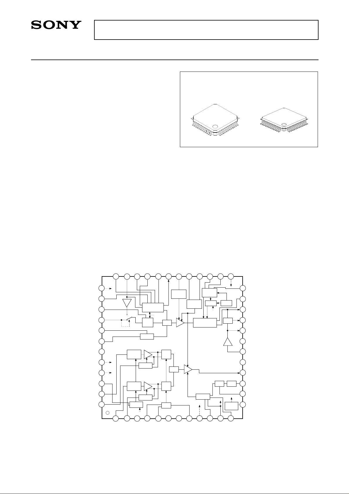
Description
The CXA1592Q/R is a bipolar IC developed as an
encoder for CCD color cameras.
Color difference and luminance signals are input
to be output as composite video and Y/C separate
signals.
The CXA1592 is a variant of the CXA1392 in
which the down/up ratio and level of shapness
signal have been changed from 1 : 3 to 1.5 : 1.5.
Features
• Carrier balance adjustment unnecessary
(Carrier leak above 36 dB against burst)
• High S/N
• Low power consumption (140mW)
Applications
CCD camera
CXA1592Q/R
CXA1592Q
48 pin QFP (Plastic)
Structure
Bipolar silicon monolithic IC
Operating Conditions
• Supply voltage VCC 4.75 to 5.25 V
• Ambient temperature Topr –20 to +75 °C
CXA1592R
48 pin LQFP (Plastic)
Absolute Maximum Ratings (Ta = 25°C)
• Supply voltage VCC 7V
•Storage temperature Tstg –65 to +150 °C
• Allowable power dissipation PD 600 mW
Block Diagram and Pin Configuration
SHPLEVEL
YTBLK
NOISESLICE
YHCLP
YHIN
YL-YHCLP
YL-YHIN
AGND
CLP4
CLP2
DLE
36
35
37
38
39
40
41
42
43
44
45
1/2
BURST
CLP4
SHPCLP1
34
HAP GAIN
SLICE BLK
CLP4
BLK
CLP4
3/2
CLP2
DLD
SHPCLP2
32
33
YTBLK
MOD
31
ADO
BLK
SHPOUT
30
LEVEL
CONT
GC
1.4 TYP
2/3 TYP
ADO
YLEVEL
FADERMODE
29
LEVEL
CONT
CLP2 WC
SETUP SYNC
GC
SETUPLEVEL
FADERSIG
28
27
LEVEL
CONT
LOGIC REF V
SYNC
C BLK
SYNCLEVEL
25
26
ADO
×1.6
SYNC
24
WCLEVEL
23
SETUPCLP
22
YOUT
VOUT
21
20
CHROMA
19
DGND
18
CIN
17
AV
16
COUT
CC
BLEVEL
B-YIN
B-YCLP
46
47
48
1
R-YIN
CLP4
BURST
B.GEN
2
R-YCLP
BFG
3
CC
DV
3/2
CLP2
4
4FSCIN
5
MOD
BLK
LALT
1/4
6
NC1
7
NC2
8
FSCOUT
LOGIC
9
BFG
10
11
BF
CBLK
CLP4ADO
MODE
GEN
12
CTBLK
15
14
13
CSY
CSAGC
MODE
Sony reserves the right to change products and specifications without prior notice. This information does not convey any license by
any implication or otherwise under any patents or other right. Application circuits shown, if any, are typical examples illustrating the
operation of the devices. Sony cannot assume responsibility for any problems arising out of the use of these circuits.
– 1 –
E91537A78
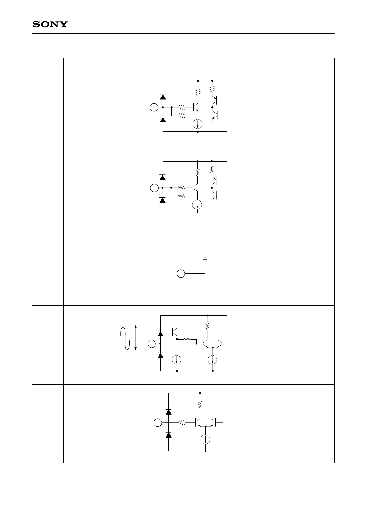
Pin Description
Pin No.
1
R-Y IN 3V
Symbol Pin voltage Equivalent circuit Description
AVCC
1k
140
1
2k
R-Y signal input pin.
Clamped internally through
C cut input.
140
10µA
AGND
CXA1592Q/R
AVCC
1k
2
R-Y CLP
3.4V
2
140
2k
Pin connecting the capacitor
for R-Y modulator clamp.
Setting the capacitance to
too small a value will enlarge
the carrier leak.
140
3
DVCC 5V
3
14.32MHz
20k
4
4FSCIN
4
1Vp-p
DC 2.5V
10µA
AGND
DVCC
DVCC
1k
80µA80µA
DGND
0.1µF and above is
recommended.
Power supply pin for the 1/4
counter block.
Input pin for the 4FSC used
to make up the Sub Carrier.
Input through C cut.
Set amplitude to over
500mVp-p.
DVCC
1k
140
5
LALT 0V
5
Input pin for Line Alternate
signal during PAL mode.
VTH is at 2.5V. Input a pulse
with an amplitude larger than
VTH ±0.5V.
80µA
DGND
Set to GND during NTSC
mode.
– 2 –

CXA1592Q/R
Pin No.
6
Symbol Pin voltage Equivalent circuit Description
NC1 —
7 NC2 —
8
9
FSCOUT 5V
BFG
5V
0V
Not for use.
Keep open
Not for use.
Keep open.
DVCC
200
Outputs a sub carrier with
the same phase as B-Y.
When not in use, connection
140
8
to VCC prevents output and
allows for 600µA of current
saving.
500µA
DGND
Determining phase to 4FSC
is impossible.
Inserts a pulse slightly larger
AVCC
1k
140
9
40µA
AGND
than BF on both ends.
BF
BFG
VTH is at 2.5V. Input a pulse
with an amplitude larger than
VTH ±0.5V.
10
11
BF
CBLK
5V
5V
0V
0V
10
11
140
140
1k
1k
40µA
AVCC
20µA
AGND
AVCC
AGND
Inputs BF (burst flag) pulse.
During analog burst, the
input pulse smoothens the
waveform.
The input pulse waveform
becomes the envelope of the
analog burst waveform.
3.5V
2.5V
During the usual burst, be
sure to input the pulse.
Inputs CBLK
(composite blanking) pulse.
VTH is at 2.5V. Input a pulse
with an amplitude larger than
VTH ±0.5V.
– 3 –

CXA1592Q/R
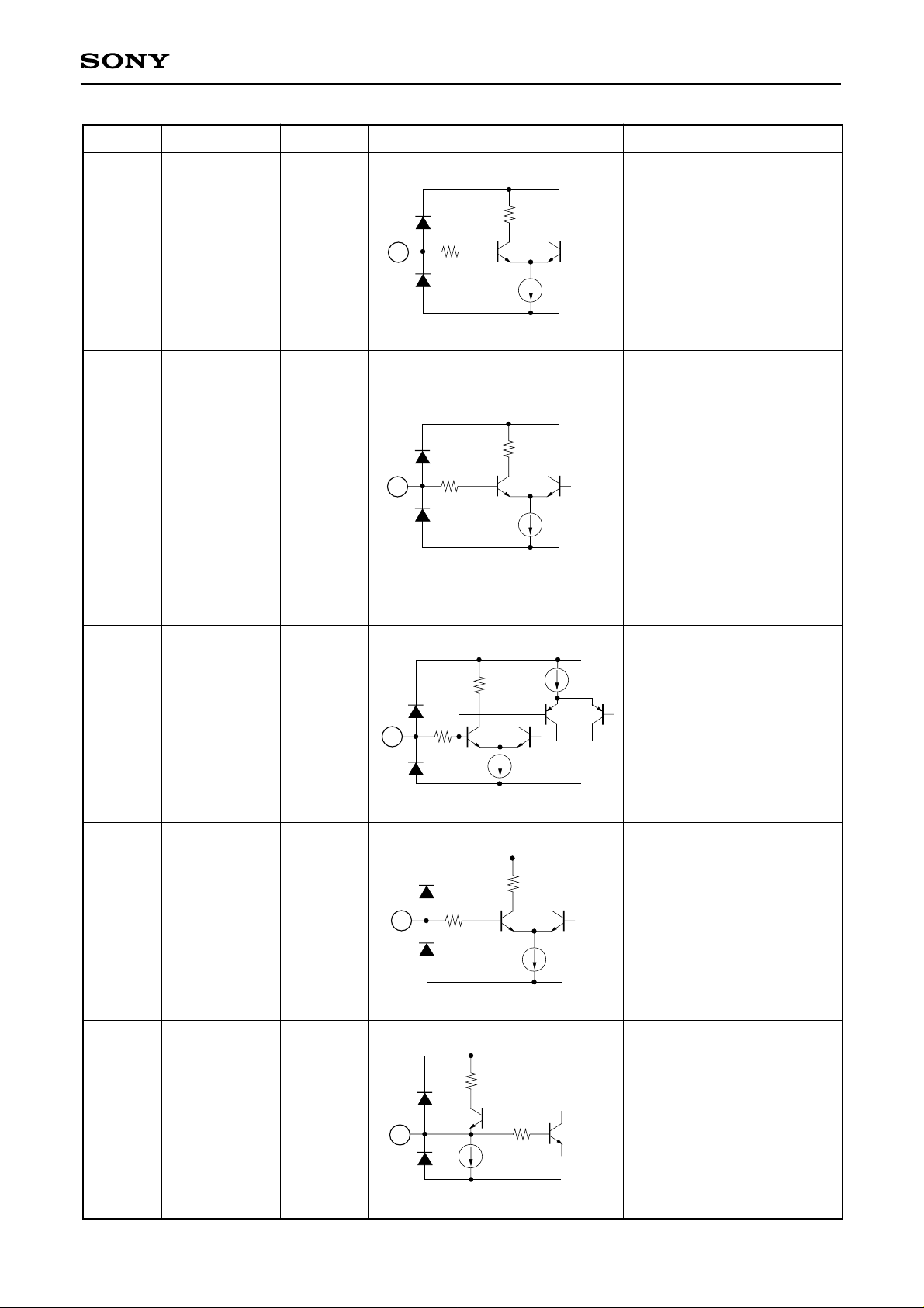
Pin No.
12
13
14
Symbol Pin voltage Equivalent circuit Description
Inputs CT (chroma titler) pulse.
This signal prevents the
application of chroma
suppress during the titler
signal period.
VTH is at 2.5V. Input a pulse
with an amplitude larger than
VTH ±0.5V.
CTBLK
5V
AVCC
1k
140
12
0V
80µA
AGND
Selected NTSC, PAL or
NTSC × 2, PAL × 2 modes.
0V : NTSC × 1 Normal
2.5V: NTSC × 2 Analog
3.5V: PAL × 2 Analog
5V : PAL × 1 Normal
Suppresses chroma signal at
the AGC gain control signal.
MODE 0V
CSAGC 0V
AVCC
1k
140
13
60µA
AGND
AVCC
1k
140
14
3V (100%) to 4.2V (50%)
40µA
AGND
burst
burst
burst
burst
15
16
CSY
2.4V
COUT 2.8V
15
16
140
140
10µA
1k
200
1500µA
2k
AVCC
Suppresses chroma signal at
the Y signal.
200mV (100%) to 700mV
(0%)
Inputs at C cut. Clamped
internally.
AGND
AVCC
Chroma signal output pin.
Output as rectangular waves.
AGND
– 4 –

CXA1592Q/R
Pin No.
17
18
Symbol Pin voltage Equivalent circuit Description
AVCC
AVCC
5V
17
AVCC
Power supply pin for other
than 1/4 counter block.
Input pin for chroma signal
passed through BPF.
Internally biased with a 20kΩ
resistance.
CIN 2.5V
20k
18
Input at C cut.
AGND
19
20
21
DGND 0V
CHROMA
VOUT
2V
1.8V
20
21
19
200
600µA
200
600µA
DGND
140
AVCC
AGND
AVCC
AGND
GND pin for 1/4 counter
block.
Signals input from CIN are
amplified and output through
this pin.
Chroma signal output pin
when used for Y/C separation
output.
Output pin of composite
video signal.
When not in use, connection
to VCC allows for 900µA of
current saving.
– 5 –

CXA1592Q/R
Pin No.
22
23
24
Symbol
YOUT
Pin voltage Equivalent circuit Description
2.4V
SETUPCLP 3.3V
WC LEVEL 3.4V
24
23
22
140
140
140
AVCC
200
Y signal output pin when
used for Y/C separation
output.
600µA
AGND
AVCC
2k
1k
Connecting pin for the white
clip clamp capacitor.
Over 0.1µF is recommended.
10µA
AGND
AVCC
1k
White clip level control pin.
1.6V (550mV) to 5V
(1110mV)
80µA
AGND
25
26
5V
SYNC
SYNC LEVEL 0V
0V
25
26
140
140
1k
1k
80µA
AVCC
Sync pulse input pin.
VTH is at 2.5V. Input a pulse
with an amplitude larger than
VTH ±0.5V.
AGND
AVCC
Sync level control pin.
1.6V (180mV) to 5V (380mV)
0V (287mV) preset.
40µA
AGND
– 6 –
CXA1592Q/R
Pin No.
27
28
Symbol Pin voltage Equivalent circuit Description
AVCC
1k
SETUP LEVEL
3.5V
140
27
80µA
AGND
Set up level control pin.
2.4V (0mV) to 5V (120mV)
Controls the signal suppress
level during Black Fader.
Controls the signal suppress
level during White Fader and
at the same time controls the
set up level.
Signal suppress control:
FADER SIG 0V
AVCC
1k
140
28
2V (100%) to 2.9V (0%)
20µA
AGND
Set up level control:
2V (0%) to 2.9V (100%)
Black Fader/White Fader
mode selection executed
through Fader Mode pin.
29
30
31
FADER MODE
Y LEVEL
3.5V
3.4V
SHP OUT 3V
29
30
31
140
140
1k
200
600µA
40µA
140
1k
AVCC
20µA
AGND
AVCC
80µA
AGND
AVCC
AGND
Black Fader and White
Fader mode select pin.
Also conrols the final value
(100%) of White Fader white
level (set up level).
0V (Black Fader)
1.8V (100mV) to 5V (630mV)
(White Fader)
Y signal level control pin.
1.6V (–3.5dB) to 5V (9dB)
Aperture signal output pin.
When not in use, connection
to VCC allows for 700µA of
current saving.
– 7 –
 Loading...