

Sony CXA1562S, CXA1562M, CXA1561S, CXA1561M, CXA1560S Datasheet
CXA1560S, CXA1561M/S, CXA1562M/S
Dolby∗B-C Type Noise Reduction System
Description
The CXA1560 series is a bipolar IC incorporating
stereo Dolby B-C type noise reduction (NR) system.
Five kinds of device are provided due to the
combination of three line output levels and two
packages for various applications.
A reduction in the number of external parts and
small package have been achieved due to the fact
that the spectral skewing circuits are all on-chip.
Features
• Few external parts
• Spectral skewing circuit are on-chip
• NR ON/OFF, REC/PB, MPX filter ON/OFF switches
• Small package (24-pin SOP, 22-pin SDIP)
• Low current consumption 13mA Typ.
(power supply ±6V)
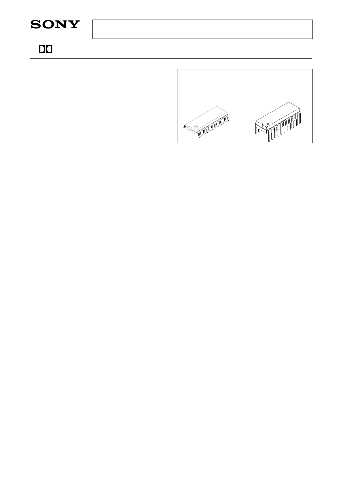
Structure
Bipolar silicon monolithic IC
CXA1561M
CXA1562M
24 pin SOP (Plastic)
CXA1560S
CXA1561S
CXA1562S
22 pin SDIP (Plastic)
Absolute Maximum Ratings (Ta = 25°C)
• Supply voltage Vcc – VEE 17 V
• Operating temperature Topr –40 to +85 °C
• Storage temperature Tstg –65 to +150 °C
• Allowable power dissipation PD 600 (SOP) mW
1200 (SDIP) mW
∗
This IC is available only to the licensees of Dolby Laboratories Licensing Corporation from whom licensing and applications
information may be obtained.
∗
"Dolby" and the double D symbols are trademarks of Dolby Laboratories Licensing Corporation.
Sony reserves the right to change products and specifications without prior notice. This information does not convey any license by
any implication or otherwise under any patents or other right. Application circuits shown, if any, are typical examples illustrating the
operation of the devices. Sony cannot assume responsibility for any problems arising out of the use of these circuits.
– 1 –
E93805B5X-PP
CXA1560S, CXA1561M/S, CXA1562M/S
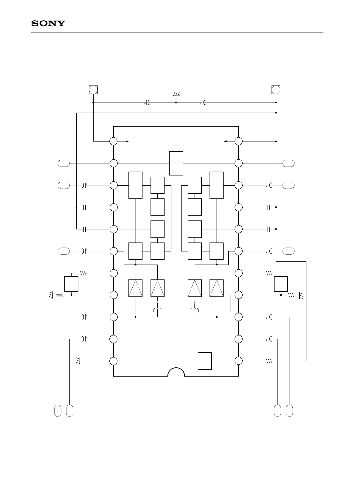
P3 MODE
P14 RECOUT1
P13 LINEOUT1
C16
C15
C14
C13
1µ
68n
100n
1µ
VCC
P2
12
CC
V
13
MODE
14
RECOUT1
15
TCL1
16
TCH1
17
LINEOUT1
CC
V
REC AMP
SSK
C1
10µ
HLS HDET LDET LLS
Mode
Control
HLS HDET LDET LLS
C2
10µ
VEE
SSK REC AMP
11
10
9
8
7
6
EE
V
NRSW
TCL2
TCH2
VEE
P1
1µ
C26
RECOUT2
68n
C25
C24
100n
1µ
C23
LINEOUT2
P5
P24
P23
NRSW
RECOUT2
LINEOUT2
MPX
R12
6.8k
P12
P11
PBIN1
LINEIN1
Filter
R11
C12
C11
3.3k
1µ
1µ
18
MPXOUT1
19
MPXIN1
20
LINEIN1
21
PBIN1
22
VCT
MOA
MOA
IREF
R21
5
4
3
2
PBIN2
1
IREF
MPXOUT2
MPXIN2
1µ
C22
LINEIN2
1µ
C21
R1
3.3k
20k
MPX
Filter
P22
PBIN2
R22
6.8k
P21
LINEIN2
For SOP package, refer to the Pin
Description or Application Circuit.
Block Diagram and Pin Configuration
Note) This figure shows SDIP package.
– 2 –
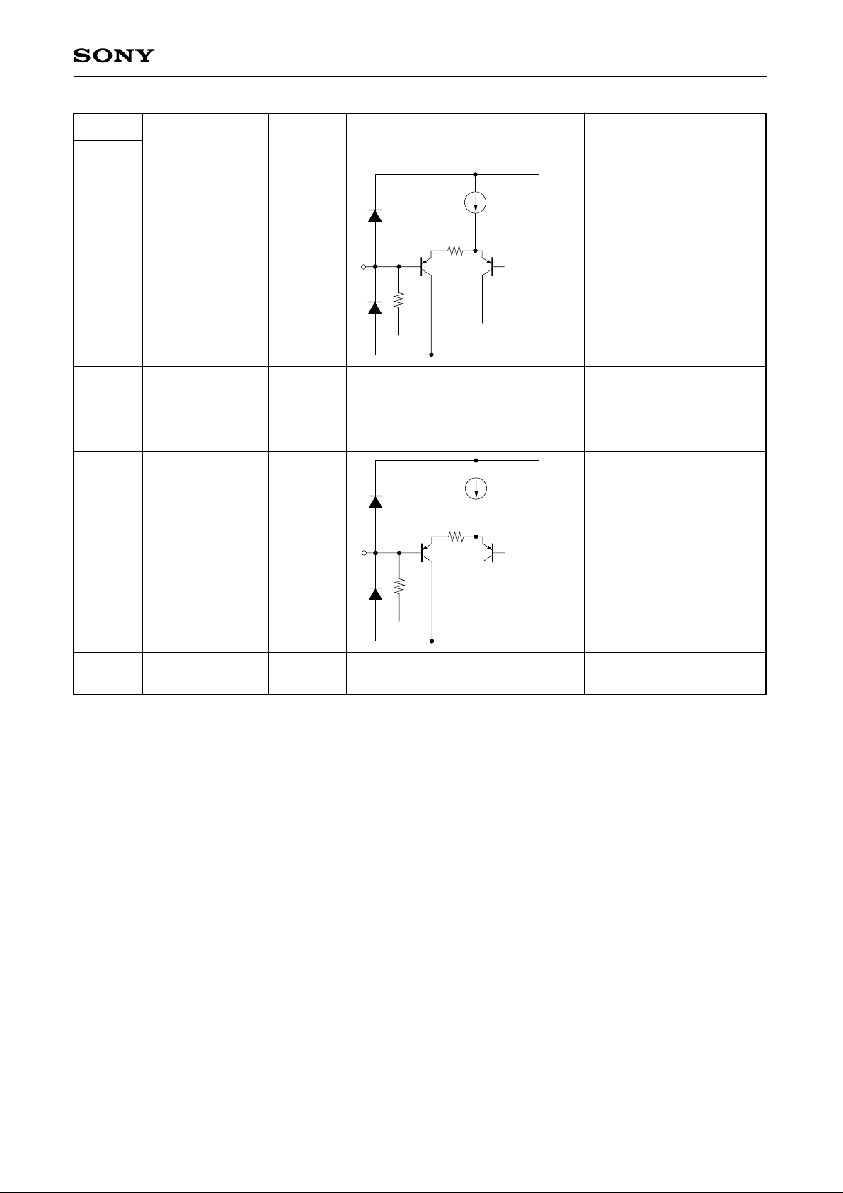
Pin Description and Equivalent Circuit
CXA1560S, CXA1561M/S, CXA1562M/S
Pin No.
SOP
1
2, 23
SDIP
Symbol
1 IREF 0
2, 21
PB IN
MPX IN
4, 194, 21
Z: Imp
40K
VDC (V)
VEE + 1.25V
VCT
Equivalent circuit Description
CC
V
Reference current pin for
setting internal filter cut-off
VEE + 1.25V
VEE
VCC
frequency
Playback input pin
VCT
40k
Reference level = –30dBm
Buffer amplifier input pin to
drive multiplex filter
Reference level = –19dBm
VEE
3, 22 3, 20
5, 18
5, 20
LINE IN
MPX OUT
62K
0
VCT
VCT
62k
500
5008.8k
VCC
VCT
Recording input pin
Reference level = –25dBm
VEE
VCC
Buffer amplifier output pin
to drive multiplex filter
Reference level = –15dBm
VEE
– 3 –
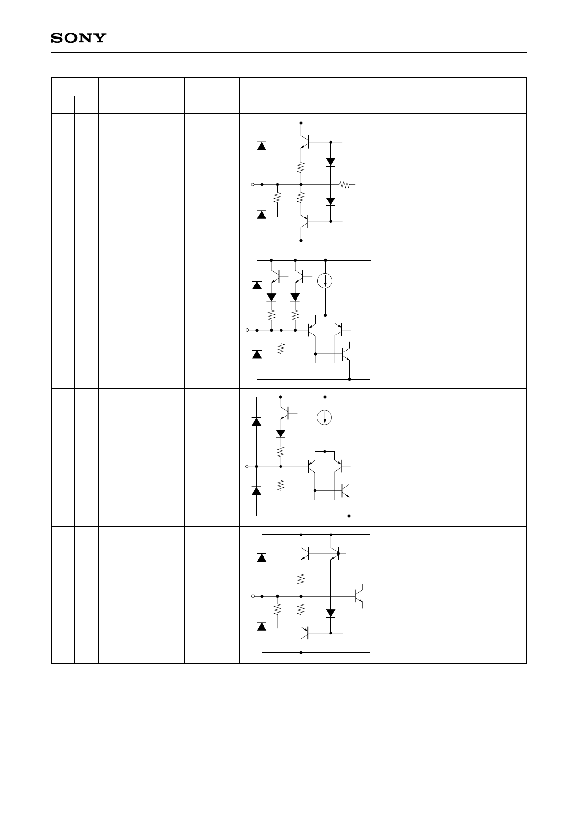
CXA1560S, CXA1561M/S, CXA1562M/S
Pin No.
SOP
6, 19
7, 15
SDIP
6, 17
7, 16
Symbol Equivalent circuit Description
LINE OUT 0
TCH
Z: Imp
—
VDC (V)
VCT
VEE + 0.4V
13k 36k
330k
200
200
VCC
VEE
V
Line output pin
CC
Time constant connecting
pin for HLS detector
8, 17
9, 16
8, 15
9, 14
TCL
REC OUT
—
0
VEE + 0.4V
VCT
13.5k
480k
200
200
VEE
V
VEE
VCC
VEE
CC
Time constant connecting
pin for LLS detector
Recording output pin
Reference level = –6dBm
– 4 –
CXA1560S, CXA1561M/S, CXA1562M/S
Pin No.
SOP
10
11 11
14
15 13
SDIP
10
12
Symbol Equivalent circuit Description
Z: Imp
VDC (V)
VCC
50µA
NR control pin
NRSW
——
22k
50k
VEE
H: C type
M: B type
L: NR OFF
Dual power supply: VEE
VEE
VCC
VEE
VCC
VCC
50µA
Single power supply:
Vcc
MODE control pin
MODE
——
22k
50k
H: REC (Filter ON)
M: REC (Filter OFF)
L: PB
GND pin
24
22
VCT
VEE
0
VCT
Dual power supply: GND
Single power supply: Vcc/2
– 5 –
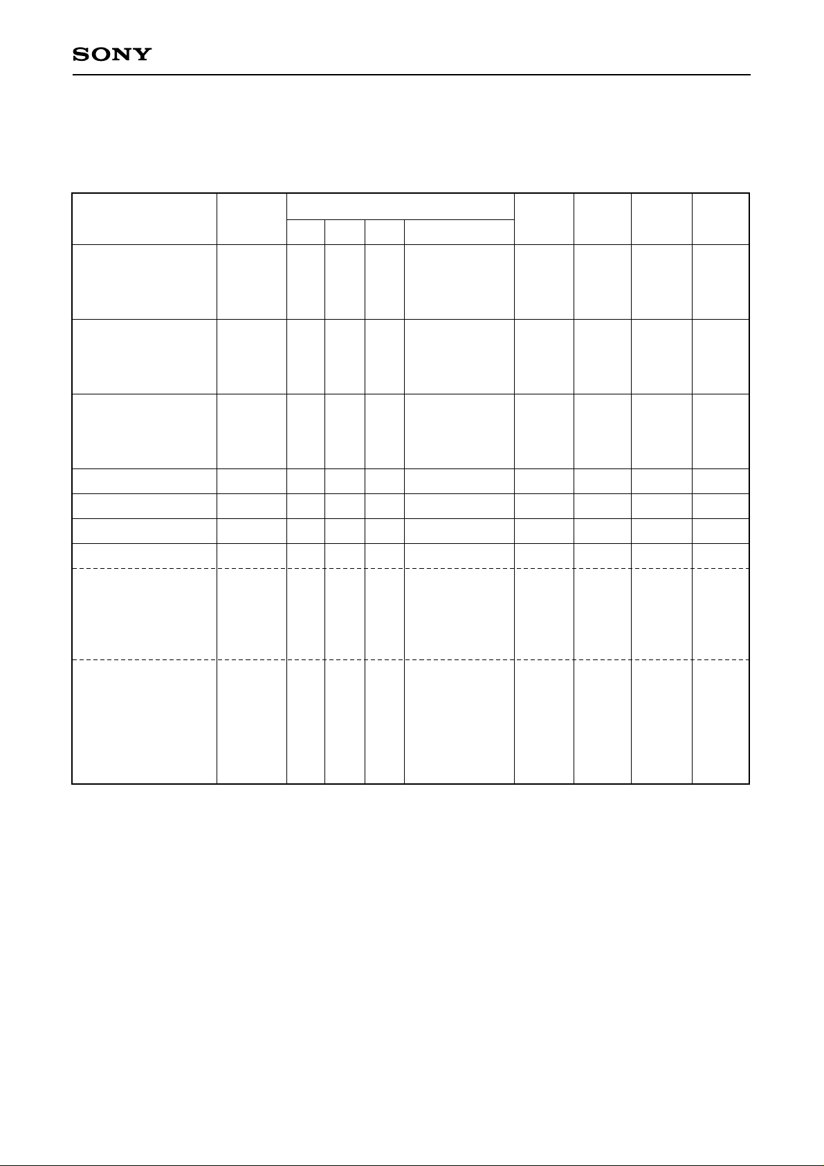
Electrical Characteristics
Ta = 25°C, Dolby level: –6dBm (= 388mVrms) at REC OUT,
VCC = 15V (CXA1560), VCC = 12V (CXA1561), VCC = 9V (CXA1562)
CXA1560S, CXA1561M/S, CXA1562M/S
Characteristics
Operating voltage
CXA1560
CXA1561
CXA1562
Current consumption
CXA1560
CXA1561
CXA1562
LINE OUT level
CXA1560
CXA1561
CXA1562
LINE IN level
PB IN level
MPX amplifier gain
Encode characteristics
B type boost
(1)
(2)
(3)
(4)
Symbol
Vopr
ICC
Vlout
Vlin
Vpin
Gmpx
B-R-1
B-R-2
B-R-3
B-R-4
Measurement conditions
NR f (Hz)
R/P
—
—
—
REC
REC
REC
PB
MPX
REC
REC
REC
REC
OFF
OFF
OFF
OFF
OFF
—
1k
1k
1k
1k
B
500
B
5k
B
10k
B
10k
∗
Other conditions
No Signal
–25dB
–25dB
–40dB
0dB
Min. Typ. Max.
11.5
8.5
7.2
8.0
8.0
8.0
–1.0
–4.0
–7.0
–27
–32
9.0
1.4
3.9
9.7
–1.1
—
—
—
13.2
13.0
12.8
0.0
–3.0
–6.0
–25
–30
10.0
2.9
5.4
10.4
0.4
16.0
16.0
16.0
18.0
18.0
18.0
1.0
–2.0
–5.0
–23
–28
11.0
4.4
6.9
11.4
1.9
Unit
V
V
V
mA
mA
mA
dBm
dBm
dBm
dBm
dBm
dB
dB
dB
dB
dB
C type boost
(1)
(2)
(3)
(4)
(5)
(6)
C-R-1
C-R-2
C-R-3
C-R-4
C-R-5
C-R-6
REC
REC
REC
REC
REC
REC
C
500
C
500
C
2k
C
2k
C
5k
C
10k
–60dB
–25dB
–60dB
–25dB
–25dB
0dB
14.2
7.2
18.7
5.4
3.5
–5.5
16.2
9.2
20.7
7.4
5.5
–3.5
18.2
11.2
22.7
9.4
7.5
–1.5
dB
dB
dB
dB
dB
dB
– 6 –
 Loading...