

Sony CXA1553P, CXA1553M, CXA1552P, CXA1552M, CXA1551P Datasheet
...
—1—
E92315A79-TE
Sony reserves the right to change products and specifications without prior notice. This information does not convey any license by
any implication or otherwise under any patents or other right. Application circuits shown, if any, are typical examples illustrating the
operation of the devices. Sony cannot assume responsibility for any problems arising out of the use of these circuits.
Absolute Maximum Ratings (Ta=25 °C)
• Supply voltage VCC 23 V
• Operating temperature Topr –40 to +85 °C
• Storage temperature Tstg –65 to +150 °C
• Allowable power dissipation
PD
SOP16 (A1551M/A1552M/A1553M) 500 mW
DIP16 (A1550P/A1551P/A1552P/A1553P) 900 mW
∗These ICs are available only to the licensees of
Dolby Laboratories Licensing Corporation from
whom licensing and applications information may
be obtained.
∗“Dolby” and the double D symbols are trade marks
of Dolby Laboratories Licensing Corporation.
Description
The CXA1550/CXA1551/CXA1552/CXA1553 are
bipolar ICs providing two separate Dolby B type
noise reduction processors. The series is
composed of seven devices having four Dolby levels
and two types of package for various applications.
These devices feature very few external
components, which is achieved by monolithic filter
circuits using integrated thin film capacitors with high
capacitance.
Features
• Pin replaceable with CXA1100 series
• Minimum number of external components
• NR ON/OFF/Double Speed, REC/PB switches
included
• Small package (16 pin SOP, 16 pin DIP)
• Low current consumption 5.6mA typ.
• Dual channel processors in one chip
• Double speed encode and decode functions are
provided.
Dolby B∗type Noise Reduction System
CXA1551M/CXA1552M CXA1550P/CXA1551P
CXA1553M CXA1552P/CXA1553P
16 pin SOP (Plastic) 16 pin DIP (Plastic)
CXA1550P, CXA1551M/P
CXA1552M/P, CXA1553M/P
—2—
CXA1550P, CXA1551M/P, CXA1552M/P, CXA1553M/P
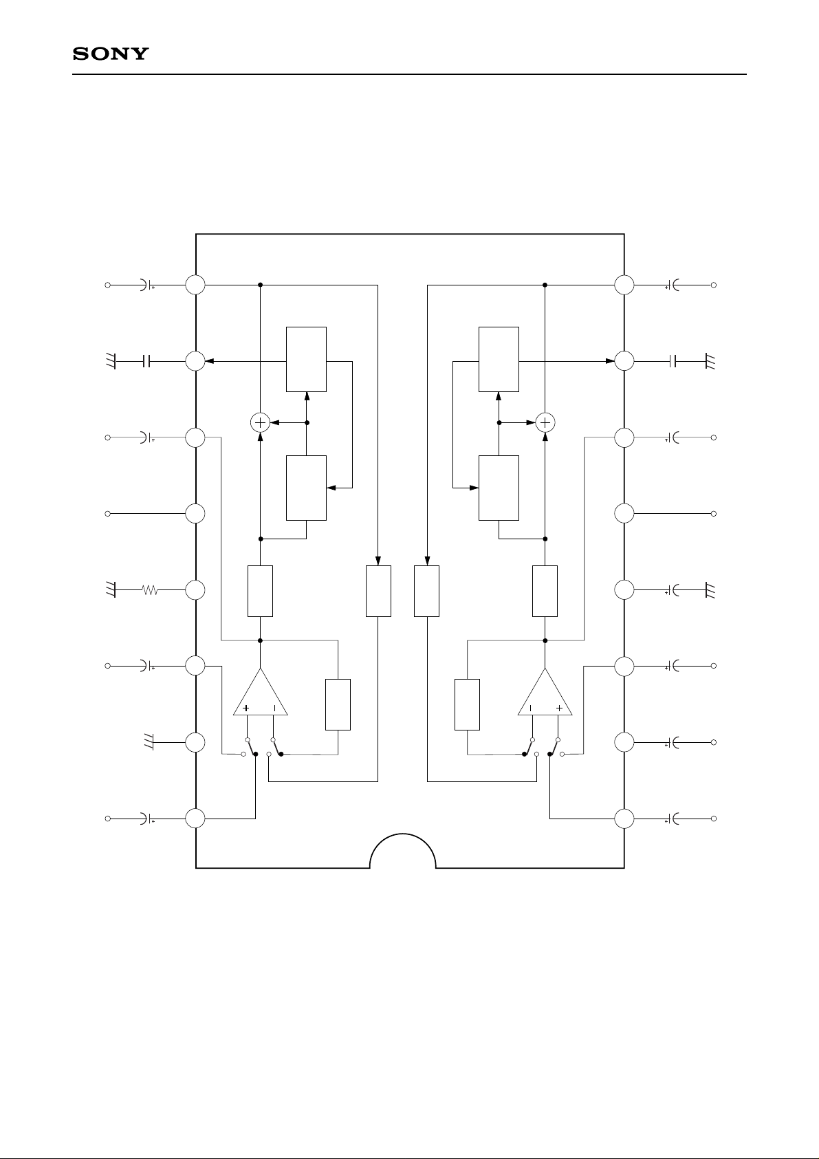
Block Diagram
10
111213141516
REC OUTLINE OUTREC/PBPB INREC IN
C12
2.2µ
C10
0.1µ
C8
2.2µ
C5
1µ
C2
1µ
R1
18k
ATT1
SC DET
ATT3
ATT2
REC OUTLINE OUTON/OFF/×2PB INVCCREC IN
C9
0.1µ
C11
2.2µ
C7
2.2µ
C4
1µ
C6
2.2µ
C1
1µ
C3
100µ
ATT1
SC DET
ATT3
ATT2
1 2 3 4 5 6 7 8
REC
IN 1
GND
PB IN 1
IREF
MODE SW
LINE
OUT 1
TC 1
REC
OUT 1
REC
IN 2
V
CC/2
V
CC
PB
IN 2
NR SW
LINE
OUT 2
TC 2
REC
OUT 2
9
ATT
SC
DET
: Attenuator
: Side Chain
: Detector

—3—
CXA1550P, CXA1551M/P, CXA1552M/P, CXA1553M/P
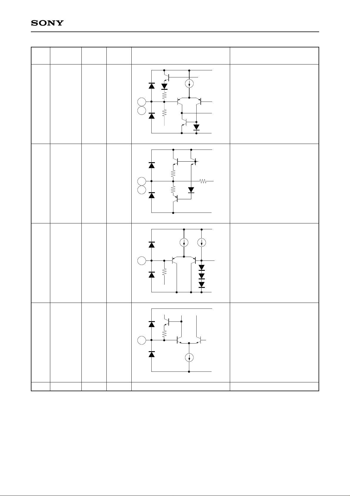
Pin Description and Equivalent Circuit (Ta=25 °C, VCC=12 V, single supply, no signal)
Pin
Symbol Z (in)
VDC
Equivalent circuit Description
No. (V)
1, 16
2
3, 14
4
5
6, 11
REC IN
VCC
PB IN
VCT
NRSW
LINE OUT
40 k
—
40 k
2 k
—
—
6.0 V
12.0 V
6.0 V
6.0 V
—
6.0 V
VCC
VCC/2
GND
40k
1
16
VCC
VCC/2
GND
40k
3
14
VCC
GND
50k
50µA 50µA
5
VCC
GND
200
200
6
11
Recording (encode) input pin
VCC power supply pin
Playback (decode) input pin
VCC/2 output pin
NR control pin
H : Double speed
M : NR off
L : NR on
Line (decode) output pin
—4—
CXA1550P, CXA1551M/P, CXA1552M/P, CXA1553M/P
Pin
Symbol Z (in)
VDC
Equivalent circuit Description
No. (V)
7, 10
8, 9
12
13
15
TC
REC OUT
MODE
IREF
GND
—
—
—
—
—
0.3 V
6.0 V
—
1.2 V
0 V
VCC
GND
600k
4.5µA
20k
7
10
VCC
GND
300
10k
300
8
9
VCC
GND
50k
50µA 50µA
12
VCC
GND
50µA
8k
13
1.2V
Time constant connecting pin
Recording (encode) output pin
REC/PB (encode/decode)
control pin
H : PB
L : REC
Active filter reference current
input pin
GND pin
—5—
CXA1550P, CXA1551M/P, CXA1552M/P, CXA1553M/P
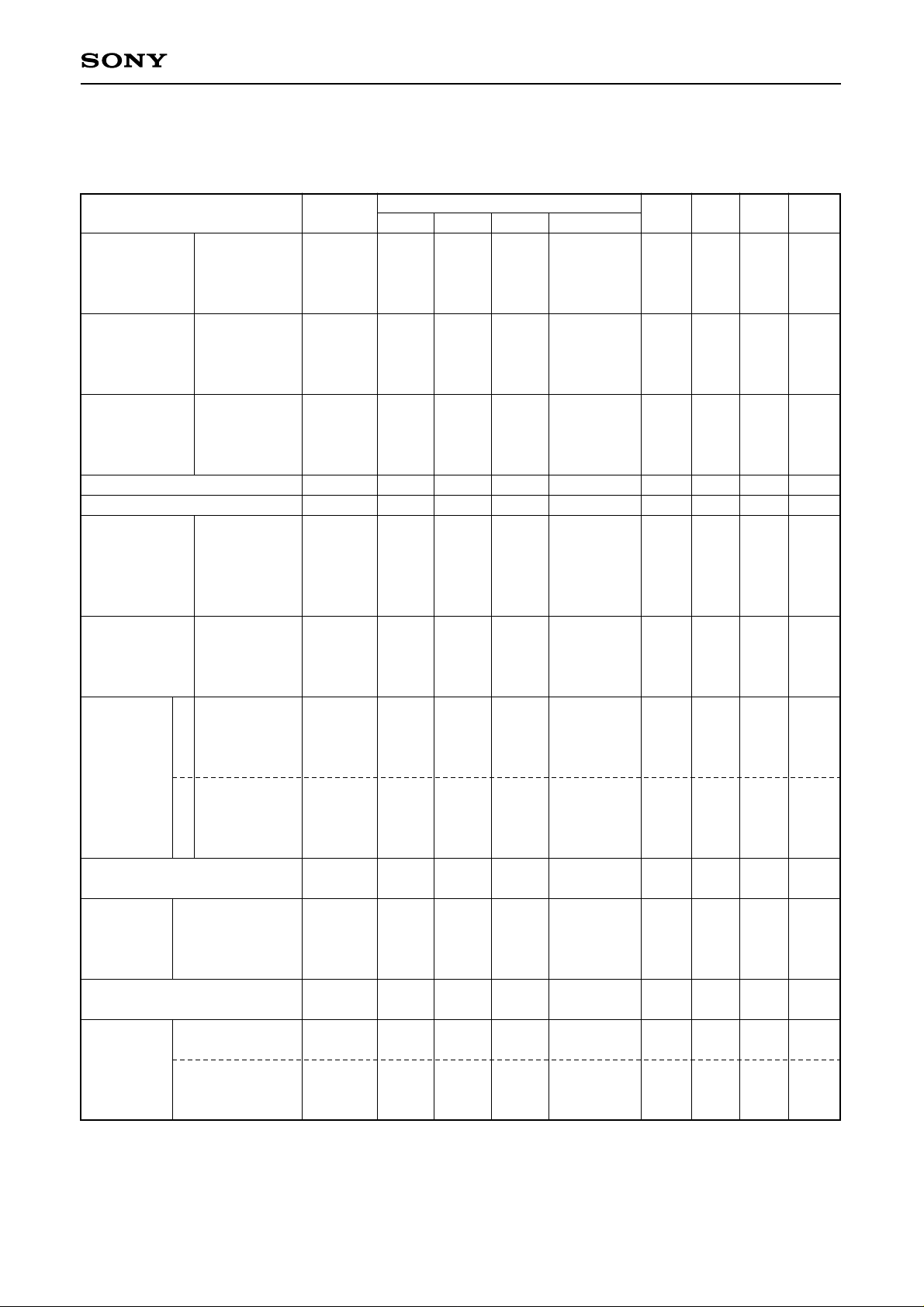
Electrical Characteristics
Ta=25 °C, Dolby Level: –10 dBm (=245 mVrms) at RECOUT, 0 dBm=775 mVrms, VCC=15 V (CXA1550),
VCC=12 V (CXA1551), VCC=9 V (CXA1552), VCC=6 V (CXA1553) unless otherwise specified
Characteristics
CXA1550
Operating CXA1551
voltage CXA1552
CXA1553
CXA1550
Current CXA1551
consumption CXA1552
CXA1553
CXA1550
LINE OUT CXA1551
level CXA1552
CXA1553
REC IN Level
PB IN Level
(1)
Encode (2)
characteristics (3)
(Boost) (4)
(5)
CXA1550
Signal CXA1551
handling CXA1552
CXA1553
CXA1550
CXA1551
Total
CXA1552
harmonic
CXA1553
distortion
CXA1550
CXA1551
CXA1552
CXA1553
Encode S/N ratio
REC-PB
Crosstalk
PB-REC
REC ch to ch
PB ch to ch
REC OUT offset voltage
(NR ON-OFF)
REC
Control
PB
voltage
ON
OFF
×2
Symbol
Vopr
I
CC
Vlout
Vrin
Vpin
B-R-1
B-R-2
B-R-3
B-R-4
B-R-5
Vomax
THD
(OFF)
THD
(ON)
SN
(CCIR)
CT-1
CT-2
CT-3
CT-4
Voff
VC-R
VC-P
VC-ON
VC-OFF
VC-×2
Test Conditions
R/P
—
REC
REC
REC
REC
REC
REC
REC
REC
REC
REC
R
NR
—
OFF
OFF
OFF
OFF
ON
ON
ON
ON
ON
OFF
OFF
ON
ON
f (Hz)
—
—
1 k
1 k
1 k
500
2 k
5 k
10 k
10 k
1 k
—
other
Signal
handling
≥12 dB
No signal
–25 dB
–25 dB
–25 dB
–40 dB
0 dB
THD=1 %
Rg=5 kΩ
(CCIR/ARM)
Min. Typ. Max. Unit
11.5 — 16.0 V
8.5 — 16.0 V
6.5 — 16.0 V
5.0 — 16.0 V
3.5 5.6 7.7 mA
3.5 5.5 7.7 mA
3.5 5.3 7.7 mA
3.5 5.1 7.7 mA
–1.0 0.0 1.0 dBm
–4.0 –3.0 –2.0 dBm
–7.0 –6.0 –5.0 dBm
–11.0 –10.0 –9.0 dBm
–32 –30 –28 dBm
–32 –30 –28 dBm
1.4 2.9 4.4 dB
5.5 7.0 8.5 dB
3.9 5.4 6.9 dB
9.7 10.4 11.9 dB
–1.1 0.4 1.9 dB
13.5 15.3 — dB
14.0 15.9 — dB
14.0 15.9 — dB
13.0 15.0 — dB
— 0.03 0.2 %
— 0.04 0.2 %
— 0.05 0.2 %
— 0.06 0.2 %
— 0.03 0.3 %
— 0.04 0.3 %
— 0.06 0.3 %
— 0.09 0.3 %
65 69 — dB
— –82 –65 dB
— –81 –60 dB
— –70 –60 dB
— –70 –60 dB
–40 — 40 mV
0 — 0.5 V
2.5 — V
CC V
0 — 0.5 V
2.5 — VCC–2.5 V
VCC–05 — VCC V
(2) NR ON (1) NR OFF
∗ 0 dB means the level which provides the Dolby level at the recording output in the noise reduction off mode.
 Loading...