Sony CXA1538S, CXA1538N, CXA1538M Datasheet

—1—
E93313D8X
Sony reserves the right to change products and specifications without prior notice. This information does not convey any license by
any implication or otherwise under any patents or other right. Application circuits shown, if any, are typical examples illustrating the
operation of the devices. Sony cannot assume responsibility for any problems arising out of the use of these circuits.
Recommended Operating Conditions
Supply voltage VCC 2 to 9 V
Structure
Bipolar silicon monolithic IC
Description
The CXA1538M/N/S is high performance one-chip
bipolar ICs designed for FM stereo/AM radios.
These include an FM/AM front end, FM/AM IF
amplifier, FM/AM detection output and FM stereo
demodulator output.
Features
• Low current consumption
(In FM mode ID=11.0 mA, in AM mode 8.5 mA,
VCC=6.0 V)
• Built-in LED drive circuit for tuning
• Built-in LED drive circuit for stereo indicator
• Built-in muting circuit for the FM band
• Few external parts
Absolute Maximum Ratings (Ta=25 °C)
• Supply voltage VCC 14 V
• Operating temperature Topr –10 to +60 °C
• Storage temperature Tstg –55 to +150 °C
• Junction temperature Tjmax 125 °C
• Allowable power dissipation
PD CXA1538M 500 mW
CXA1538N 410 mW
CXA1538S 1050 mW
FM Stereo/AM Radio
CXA1538M CXA1538S
30 pin SOP (Plastic) 30 pin SDIP (Plastic)
Block Diagram
DETUNE
MUTING
CONTROL
TUNING IND
DC
AMP
DC
AMP
BU
AMP
BU
AMP
AUTO
BLEND
MUTING
FM IF/
DISCRI
AM IF/DET
AM FE
REGULATOR
MULTIPLEX
REGULATOR
PD 1
PD 2
1/2 COUNTER
DECODE AMP
RIPPLE FILTER
ST
IND
M/ST
SW
PLL
LPF1
PILOT
DET
LPF2
PILOT
DET
LPF2
ST
IND
VCO
CHECK
Rch
OUT
Lch
OUT
VCC RIPPLE
FILTER
AGC
AFC 1
AGC
AFC 2
GND TUNE
IND
FM IFINAM IFINBAND
SELECT
VCO
GND
PLL
LPF 2
MPX
REG VCOFMDISCRI MUTEAMOSC AFCFMOSC REGFMRF
AM RFINFM RFINFE
GND
FM/AM
FE OUT
FM FE
PD : PHASE DETECTOR
BU : BUFFER
FE : FRONT END
DET : DETECTOR
IND : INDICATOR
1 2 3 4 5 6 7 8 9 10 11 12 13 14 15
161718192021222324252627282930
CXA1538M/N/S
CXA1538N
30 pin SSOP (Plastic)
For the availability of this product, please contact the sales office.

—2—
CXA1538M/N/S
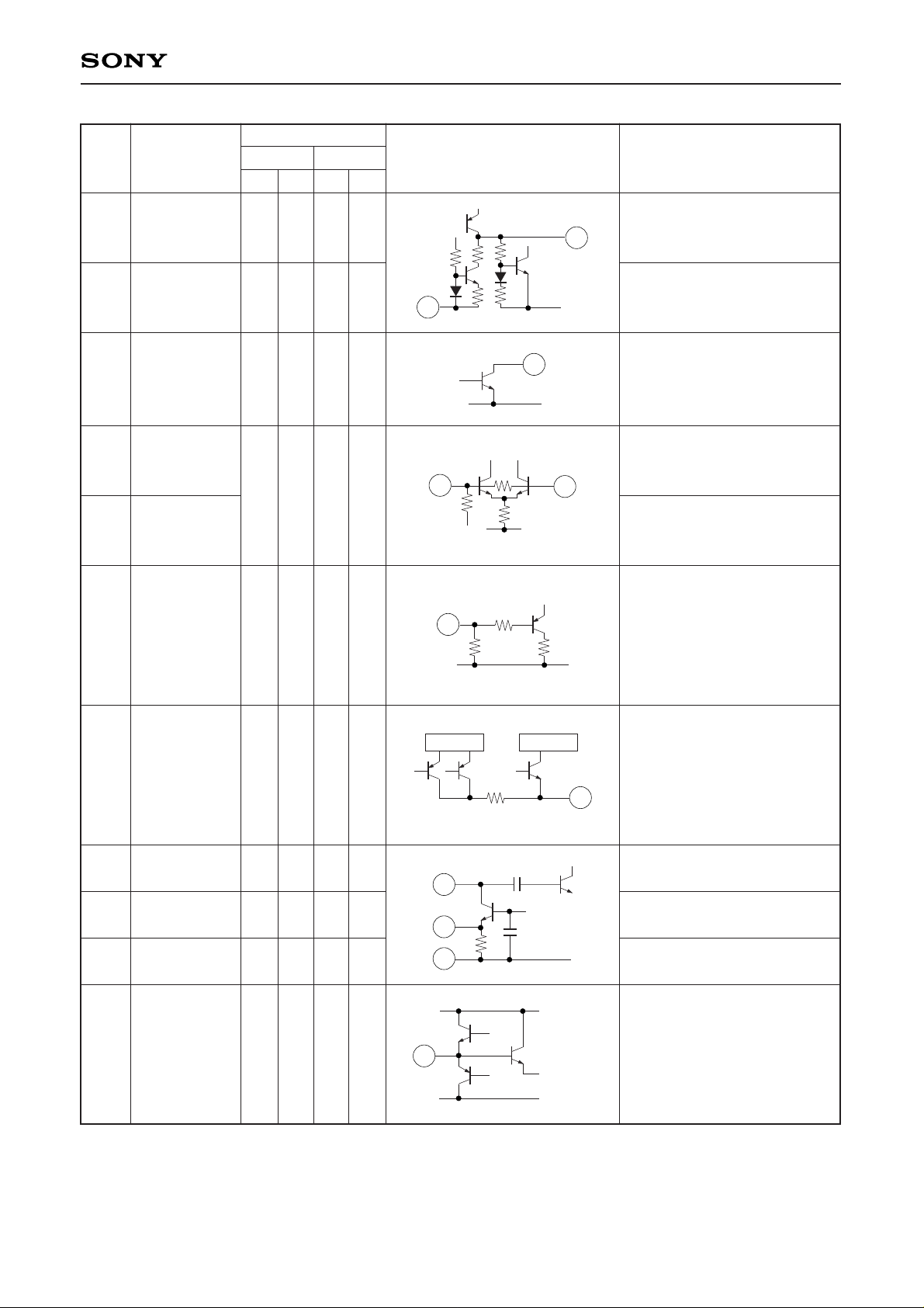
Pin Description and Equivalent Circuit
Pin Voltage (V)
No. Symbol VCC=3 V VCC=6 V Equivalent circuit Description
FM AM FM AM
1
29
2
3
4
5
6
7
8
9
10
PLL LPF1
PLL LPF2
PILOT
DET LPF1
PILOT
DET LPF2
ST IND
VCO CHECK
Rch OUT
Lch OUT
VCC
Ripple
FILTER
AGC/AFC1
AGC/AFC2
0.97 0.97 0.97 0.97
0.95 0.95 0.95 0.95
0.95 0.95 0.95 0.95
1.6 1.6 4.5 4.5
0.66 0.66 1.5 1.5
0.66 0.66 1.5 1.5
3.0 3.0 6.0 6.0
2.7 2.7 4.0 4.0
1.32 1.15 1.32 1.15
1.15 1.47 1.15 1.47
MPX REG
26k26k
129
2
3
MPX REG
6k
VCO
4
5
6
17k
17k
140k
33k
8
22k 50k
3.25k
25k
9
10
LPF for PLL
LPF’s C (1µF) for PILOT DET
inserted between pins 2 and 3
Stereo indicator drive circuit
and output for VCO check
Stereo Rch output pin
Stereo Lch output pin
Supply pin
Ripple filter
AFC pin in J band, determines time
constant of AGC in AM (depending on
external capacitor).
AFC pin in W band, determines time
constant of AGC in AM (depending
on external capacitor).

—3—
CXA1538M/N/S
Pin Voltage (V)
No. Symbol VCC=3 V VCC=6 V Equivalent circuit Description
FM AM FM AM
11
25
12
13
15
14
16
17
18
20
19
GND
MUTE
TUNE IND
FM IF IN
BAND
SELECT
AM IF IN
FM/AM
FE OUIT
FE GND
FM RF IN
FM RF
AM RF IN
0 0 0 0
0.05 0.01 0.05 0.01
1.6 1.6 4.5 4.5
1.35 0 1.35 0
0 0 0 0
0.57 0.2 0.8 0.2
0 0 0 0
0.3 0 0.3 0
1.25 1.25 1.25 1.25
1.25 1.25 1.25 1.25
11
25
12
33C
3k
13
15
1k
2k
14
AM Block FM Block
220
16
3p
1k
17
18
20
FE REG
GND
19
GND of FM/AM IF and DET
stage
Time constant for muting
provided
FM/AM tuning indicator drive
circuit
FM IF input pin
FM/AM band switching pin :
AM at GND and FM at OPEN
AM IF input pin
AM/FM IF output pin to
connect with IF filter
GND of FM/AM front end
FM RF amplifier circuit for FM
RF input
FM RF amplifier circuit to
connect to RF tank circuit
AM RF input to connect to bar
antenna

—4—
CXA1538M/N/S
Pin Voltage (V)
No. Symbol VCC=3 V VCC=6 V Equivalent circuit Description
FM AM FM AM
21
23
22
24
26
27
28
30
REG
AFC
FM OSC
AM OSC
FM DISCRI
VCO
MPX REG
GND
1.25 1.25 1.25 1.25
1.25 1.25 1.25 1.25
1.25 1.25 1.25 1.25
2.30 2.70 3.60 4.00
1.65 1.65 1.65 1.65
0 0 0 0
1.25V
REG
21
23
REG22REG
24
26
1k
MPX REG
27
28
30
Regulator output
Variable capacitance for AFC
FM local oscillation circuit
AM local oscillation circuit
Phase shift circuit to connect
to ceramic discriminator
VCO control pin for stereo
demodulation
Regulator for MPX
GND of MPX block

—5—
CXA1538M/N/S
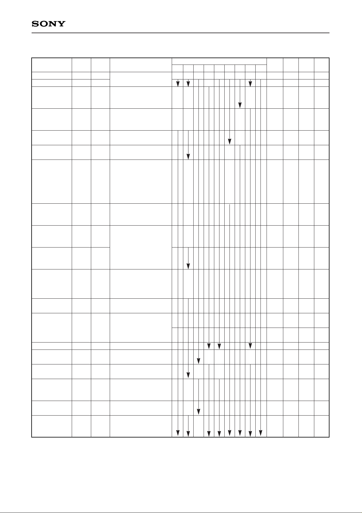
Item
Circuit current (1)
Circuit current (2)
Separation
FM MUTE
STEREO
indicator output
FM front end
voltage gain (1)
FM detection
(MONO/STEREO)
output level L, R
FM-IF
knee level
FM-IF distortion
L, R (MONO)
FM-IF distortion
L, R (STEREO)
FM-IF center
frequency
deviation
FM meter
current (1)
M/ST switching
level by IF input
Auto blend
AM front end
voltage gain (2)
AM-IF
voltage gain (4)
AM detection
output level (L, R)
AM meter
current (2)
AM detection
output distortion
(L, R)
Symbol
ID
1
ID2
SEP
A
1
Is
GV
1
VD1
VD2
THD1
∆F1
IB1
VI1
VI2
GV2
GV3
VD3
IB2
THD2
SW condition
1 2 3 4 5 6 8 9 10
A A A B A B OFF A OFF
A
A
B / B
B
ON
A A /
OFF
OFF
A
A
/ B
B
A
A
/
B
A
B B A
B A
A
/
B
A
A
Test
Point
I
D
ID
VD
VD
Is
V
A
VD
VIN3
VD
V
F
IB
Is
V
IN3
VB
VIN4
VD
IB
VD
Output waveform
and Test method
AM no signal
FM no signal
Separation when V
IN3=
50 dBµV, 10.7 MHz, 1 kHz,
22.5 kHz dev input
Attenuation of noise level
When V
IN3=no signal,
S
8 ON/OFF
V
IN3=60 dBµV, 10.7 MHz CW
Pilot ON
V
IN1=40 dBµV, 100 MHz CW
V
A=10.7 MHz CW
V
IN3=90 dBµV, 10.7 MHz
1 kHz 22.5 kHz dev
V
D=1 kHz sine wave
V
IN3=90 dBµV, 10.7 MHz
Input level at –3 dB of 1 kHz
22.5 kHz dev output
V
IN3=90 dBµV, 10.7 MHz
1 kHz 75 kHz dev
V
D=1 kHz sine wave
V
IN3=90 dBµV, 10.7 MHz CW
V
IN3=60 dBµV, 10.7 MHz CW
V
IN3=10.7 MHz
VIN2=60 dBµV, 1660 kHz CW
V
B=455 kHz CW
V
IN4 level at output of
15.5 mVrms
V
IN4=85 dBµV 455 kHz
(1 kHz 30 % MOD)
V
D=1 kHz sine wave
V
IN4=85 dBµV, 455 kHz CW
V
IN2=95 dBµV, 1660 kHz
(1 kHz 30 % MOD)
V
D=1 kHz sine wave
Electrical Characteristics (Ta=25 °C, VCC=6 V)
Min. Typ. Max. Unit
5.0 8.5 12.0 mA
7.0 11.0 15.0 mA
30 40 — dB
16 23 30 dB
1.8 3.0 5.0 mA
28 35 42 dB
35.0 77.5 138 mVrms
— 25 31 dBµV
— 0.1 2.0 %
0.1 2.0 %
–50 0 +50 kHz
1.8 3.5 7.0 mA
M
→ST
43 48 dBµV
38
ST
→M
41 46 dBµV
35
1 10 41 dB
19 24 28 dB
15 21 29 dBµV
35.0 77.5 138 mVrms
1.3 3.0 7.0 mA
— 0.6 2.0 %
V1 to
V5 input
short
0 dBµV=1 µV
 Loading...