

Sony CXA1518Q, CXA1518S Datasheet

—1—
E92604A79-TE
Sony reserves the right to change products and specifications without prior notice. This information does not convey any license by
any implication or otherwise under any patents or other right. Application circuits shown, if any, are typical examples illustrating the
operation of the devices. Sony cannot assume responsibility for any problems arising out of the use of these circuits.
Absolute Maximum Ratings (Ta=25 °C)
[Pin numbers shown are for the CXA1518S.]
• Supply voltage VCC 10 V
• Input signal
(Pin 6) VIS 0.6 Vp-p
• Control voltage
(Pins 12, 13, 14) VIC VCC V
• Operating temperature Topr –20 to +75 °C
• Storage temperature Tstg –65 to +150 °C
• Allowable power dissipation
PD 900 mW
(SDIP)
470 mW
(QFP)
• LED drive current Iled 10 mA
Operating Voltage
6.0 to 4.5 V
Description
The CXA1518Q/S are bipolar ICs designed for
EIAJ TV sound multiplexing decoders. These ICs
provide various functions including sound
multiplexing demodulation, broadcast mode
discrimination (stereo/bilingual discrimination
display), mode display, and muting.
Features
• External parts greatly reduced with a built-in active
filter.
• Count down can be used for broadcast mode
discrimination so that adjustment for discrimination
system (Q-OSC) is not required.
• Output level of 380 mVrms (1 kHz, MONO, 100 %)
• Forced monaural operates with both stereo and
bilingual broadcasts.
• Built-in digital facsimile interference elimination
filter.
• Low supply voltage (VCC=5 V)
• The pin configuration of the CXA1518S is identical
to that of the CXA1138AS.
Applications
• Color TVs
• Hi-Fi VCRs
• Liquid crystal TVs
Structure
Bipolar silicon monolithic IC
EIAJ Sound Multiplexing Decoder
CXA1518Q CXA1518S
32 pin QFP (Plastic) 22 pin SDIP (Plastic)
CXA1518Q/S

—2—
CXA1518Q/S
Block Diagram
CXA1518Q
CXA1518S
3.5fH
CLOCK
952H
Z
CLOCK
1 2
3
4
5
6
8
9
10
11
12
13
19
21
23
25
26
27
28
29
30
31
32
22
24
20
18
17
MCOUT
NCNC
NC
NC
NC
NC
CUBI
MPXIN
NC
NC
NC
MCIN
LOUT
ROUT
MOUT
MAIN
DEEM
MATRIX
SUB
MAIN
TEST
L
R
CUE
CARRIER
OUTPUTAMP &
OUTPUT
SW
MAIN
OUT
CONT
LED
DRIVE
BIAS
CURRENT
IBIAS
SUB
BPF
4.5fH
TRAP
3.5f
H
VCO
BUFFER
BIAS
VOLTAGE
INAMP
MPX SIGNAL
SCIN
SCOUT
NC
SUBI
GND
FLAJ
REFL
V
CC
FOMO
MUTE
MODE
NC
NC
LEDMAIN
LEDSUB
LEDST
COMP
FM
DEMOD
SUB
DEEM
VOLTAGE
REGULATOR
SUB
DET
I L LOGIC
2
AM
DEMOD
952HZ
BPF
CUE
BPF
7
14
15
16
1
2
3
4
5
6
7
8
9
10
11
12
13
14
15
16
17
18
1920
21
22
SUBIGND
FLAJ
REFL
V
CC
NC
NC
CUBI
LEDST
LEDSUB
LEDMAIN
MPX IN
SC OUT
SC IN
MC OUT
MC IN
L OUT
R OUT
M OUT
FOMO
MUTE
MODE
SUB
DEEM
MATRIX
FM
DEMOD
MAIN
DEEM
TEST
L
R
SUB
MAIN
MAINOUT
CUE
CARRIER
CONT
I L LOGIC
BIAS
CURRENT
SUB
BPF
SUB
DET
IBIAS
BUFFER
BIAS
VOLTAGE
IN AMP
MPX SIGNAL
3.5fH
952HZ
BPF
952H
Z
AM
DEMOD
CLOCK
CLOCK
COMP
LED
DRIVE
VOLTAGE
REGULATOR
4.5fH
TRAP
CUE
BPF
3.5fH
VCO
2
OUTPUTAMP
&
OUTPUT SW

—3—
CXA1518Q/S
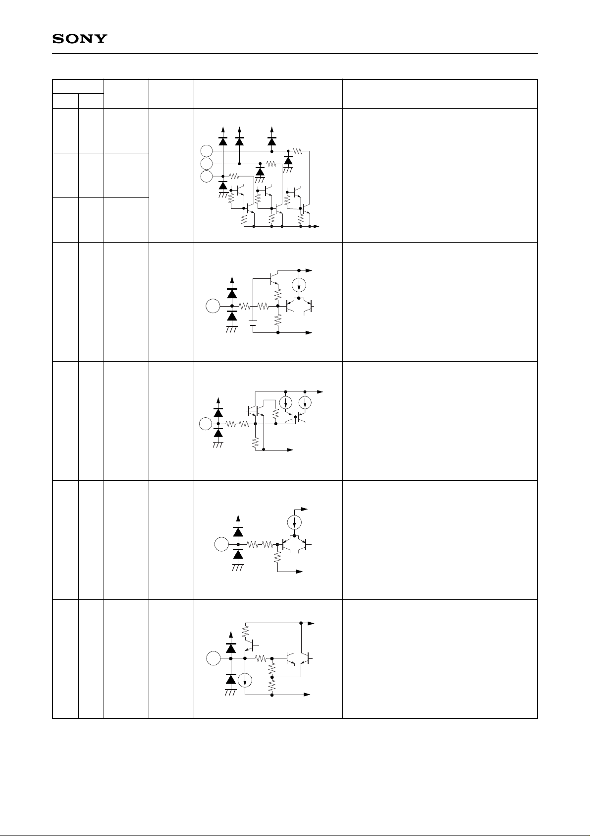
Pin Description (Ta=25 °C, VCC=5 V) Pin numbers in brackets are for the CXA1518Q.
Pin No.
Symbol
Pin
Equivalent circuit Description
SDIP QFP voltage
1
2
3
4
6
8
29
30
31
32
3
7
GND
FLAJ
REFL
VCC
MPXIN
CUBI
0
2.4 V
2.5 V
—
2.5 V
2.4 V
2
(30)
V
CC
VCC
147
10k
80k
GND
40µ
(31)
VCC VCC
54k
14k
14k
20k
1.5k
3
(3)
VCC
25k
90k
30k
GND
147
80µ
2.5V
6
8
1k
40k
11k 2k
40k
(7)
VCC VCC
147
2.5V
GND
Filter adjustment pin
Connects noise elimination filter of internal
reference power supply.
Power supply pin
Sound multiplexing signal input.
Standard input level=70 mVrms
(MONO 100 %)
Connects bias capacitor for Cue pulse
generator.
—4—
CXA1518Q/S
Pin No.
Symbol
Pin
Equivalent circuit Description
SDIP QFP voltage
9
10
11
12
13
14
15
9
10
11
14
15
16
17
LEDST
LEDSU
LEDM
MODE
MUTE
FOMO
MOUT
—
—
—
—
2.4 V
9
10
11
16k 16k 16k
64k
64k
64k
GND
VCC VCC VCC
147
147
147
(14)
V
CC
VCC
147
16k
16k
8k
2.4V
GND
20µA
12
(15)
V
CC
VCC
147
32k
160k
8k
GND
13
(16)
V
CC
VCC
80k
GND
40µ
147
1k
14
(17)
V
CC
VCC
147
14k
32k
32k
GND
15
Connects the LEDs to display each mode.
Pin 9: Stereo
Pin 10: Sub
Pin 11: Main
Switches the output mode with the DC
voltage during bilingual broadcasting.
Output mute pin.
When set to high, only DC is output from
Pins 15, 16 and 17 (Pins 17, 18 and 20).
Forced monaural pin.
When set to high, monaural function
(main) is forcibly set regardless of stereo
and bilingual broadcasts and LEDs are
extinguished.
Main signal output pin.
Always outputs the main signal component
regardless of the broadcast mode.
—5—
CXA1518Q/S
Pin No.
Symbol
Pin
Equivalent circuit Description
SDIP QFP voltage
16
17
18
19
20
21
22
18
20
22
24
25
26
28
ROUT
LOUT
MCIN
MCOUT
SCIN
SCOUT
SUBI
2.4 V
2.4 V
2.5 V
1.7 V
2.5 V
1.7 V
2.4 V
(18)
V
CC
VCC
147
14k
32k
32k
GND
16
(20)
V
CC
VCC
147
14k
32k
32k
GND
17
18
GND
V
CCVCC
VCC
147
147
147
147
(24)
(22)
16k
2.5V
160µ
80µ 80µ
20P
19
GND
V
CC VCC
VCC
147 147
147
147
20
(26)
(25)
80µA
80µA
160µA
5k
2.5V
12k
18p
21
VCC
VCC
147
147
(28)
80µ 20µ
2.5V 1.4V
16k
15k 1k 8k
64k
8k
22
R-ch output pin
L-ch output pin.
During “TEST”, outputs the Cue signal
component passed through the Cue BPF.
Connects DC cut capacitor of the main
signal.
Connects DC cut capacitor of the sub
signal.
Connects bias capacitor of the sub FM
detector.
Grounding this pin enables the TEST
mode for filter adjustment.
—6—
CXA1518Q/S
Pin No.
Symbol
Pin
Equivalent circuit Description
SDIP QFP voltage
5, 7
1, 2
4, 5
6, 8
12, 13
19, 21
23, 27
NC — —
Keep these pins open
(They are not connected to the chip.)
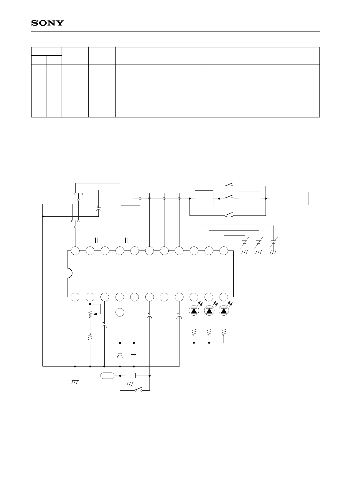
Electrical Characteristics Measurement Circuit (CXA1518S)
ON
OFF
SW6
SW4
TEST
(ON)
NORM
(OFF)
C10
10µF
C1
10µF
C3
10µF
C4
10µF
C2
47µF
C9
1µF
C10
1µF
L OUT
R OUT
MAIN OUT
22 21 20 19 18 17 16 15 14 13 12
1 2 3 4
5
6 7 8 11
15kH
Z
LPF
CCIR
FILTER
SW1
SW2
SW3
MEASUREMENT
SYSTEM
RMS
DISTORTION
DC VOLT
E2 E3 E4
VR1
20K
R1
22K
R2
470R3470R4470
E1
5V
STEREO SUB MAIN
SIGNAL
SIG
ATT
SW5
9 10
A
∗ Set ATT such that the stereo separation
(L → R) to minimum.
 Loading...