

Sony CXA1498S, CXA1498M Datasheet

CXA1498S/M
Recording/Playback Equalizer Amplifier for Stereo Tape Recorder
Description
The CXA1498S/M is a bipolar IC designed as
equalizer amplifier for tape redorder recording/
playback. This IC is particularly well-suited for double
cassette deck applications. An on-chip filter serves to
greatly reduce the number of external parts.
Features
• Recording equalizer amplifier × 2
(Monolithic filter eliminates the need for external
resonance circuit)
• AGC (automatic gain control) × 2
• Playback equalizer amplifier × 2
(Variable resistor eliminates the need for external
feedback resistor)
• Electronic switch for playback head
(Changes between A and B decks)
• Electronic switch for tape equalization
(120µs/70µs) (Independently for A and B decks)
• Electronic switch for metal tapes
• Electronic switch for normal/high speed dubbing
(Effective for both REC EQ and PB EQ)
• Recording mute function
(Soft mute is possible through use of an external
time constant circuit)
• DC controllable for fade IN/OUT
(Controls recording mute function)
• Playback mixing output pin provided
(For tune selection)
• Use of this IC simplifies the construction of double
cassette dubbing system
CXA1498S
30 pin SDIP (Plastic)
Applications
Recording/playback equalizer amplifier, playback
mixing amplifier and AGC for analog stereo tape
recorders
Structure
Bipolar silicon monolithic IC
Absolute Maximum Ratings (Ta = 25°C)
• Supply voltage VCC 12 V
• Operating temperature Topr –20 to +75 °C
• Storage temperature Tstg –65 to +150 °C
• Allowable power dissipation
PD SDIP 930 mW
Recommended Operating Condition
Supply voltage VCC 4.5 to 10.0 V
CXA1498M
30 pin SOP (Plastic)
SOP 630 mW
Block Diagram and Pin Configuration (Top View)
CC
PB IN1 (R)
30
PB IN2PB IN1
1
PB IN1 (L)
PB IN2 (R)
29
PB FB1 PB FB2
DECK
DECK- B
A/B
DECK
DECK- B
A/B
PB FB1 PB FB2PB IN2PB IN1
2
PB IN2 (L)
PB FB1 (R)
28
100k
DECK- A
DECK- A
100k
3
PB FB1 (L)
210k
PB
PB
210k
PB FB2 (R)
27
OUT
OUT
4
PB FB2 (L)
PB OUT (R)
26
PB
RFS RFC DECK
MS
PB
OUT
5
PB OUT (L)
RFS
25
BIAS &
I REF
I REF SPEED
6
MS OUT
24
7
RFC
I REF
DECK A/B
DECK A EQ
REC MUTE
VG
23
DECK
A/B
-A EQ
PB EQ
CONTROL
REC EQ
CONTROL
DECK
-B EQ METAL AGC GND
8
SPEED
22
REC
MUTE
9
DECK B EQ
21
VG AGC RECINV
30k
MUTE
CONT
VGS
AGC
TC
10
METAL
20
11
AGC TC
19
30k
AGC DET
12
AGC (R)
REC
IN
AGC (L)
18
13
Sony reserves the right to change products and specifications without prior notice. This information does not convey any license by
any implication or otherwise under any patents or other right. Application circuits shown, if any, are typical examples illustrating the
operation of the devices. Sony cannot assume responsibility for any problems arising out of the use of these circuits.
– 1 –
REC IN (R)
CC REC
VCC
REC EQ
REC EQ
GND
REC IN (L)
V
GND
OUT
REC
OUT
REC OUT (R)
16
15
REC OUT (L)
17
14
E91860C49-ST
CXA1498S/M
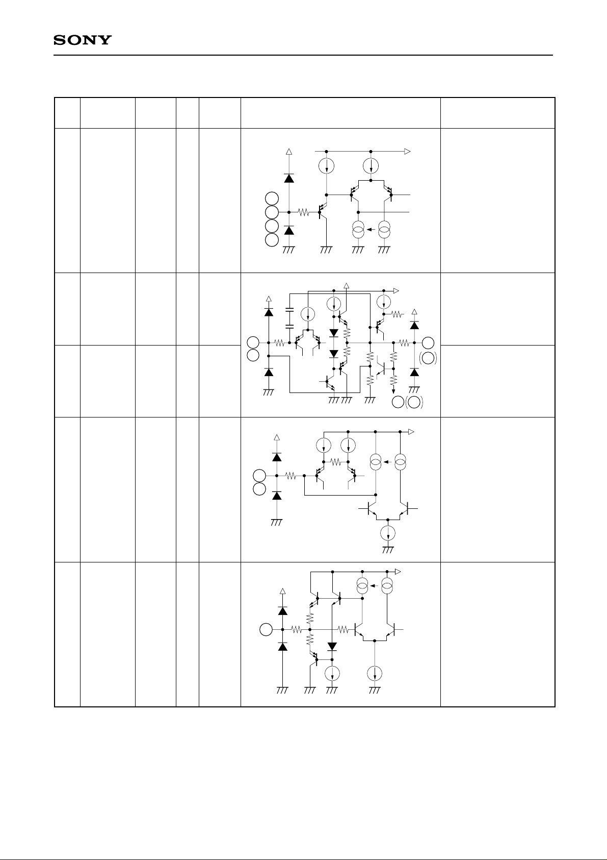
Pin Description and Equivalent Circuit (Ta = 25°C, VCC = 8V, no signal)
Pin
No.
1
2
29
30
Symbol
PBIN1 L
PBIN2 L
PBIN2 R
PBIN1 R
328PBFB1 L
PBFB1 R
526PBOUT L
PBOUT R
DC
voltage
∗1
0V
∗1
0.8V
∗1
2.5V
I/O
I/O
resistance
I—
— 68kΩ
O 147Ω
28
Equivalent circuit Description
VCC
× 6 × 6
1
147
2
29
30
GND
VCC
10p
10p
147
3
× 6 × 6
GND
× 2
V
× 3
500
500
× 6
× 4
RFS
Playback equalizer
amplifier input pins.
CC
210k
100k
To
× 5
RFS
VCC
7k
Playback equalizer
amplifier negative
feedback pins.
147
5
10k
26
Playback equalizer
amplifier output pins.
26
10k
5
427PBFB2 L
PBFB2 R
6 MS OUT
2.5V
2.5V
∗1
——
∗1
O 147Ω
27
VCC
RFS
Connection pins for
× 5 × 5
147
4
7k
the capacitor that
determines the
playback equalizer
amplifier's time
constant
(120µs, 70µs, etc.)
Mixed output pin for
the L and R outputs of
the playback equalizer
6
GND
VCC
147
500
× 2
500
5k
V
CC
amplifier.
× 4
GND
– 2 –

CXA1498S/M
Pin
No.
Symbol
DC
voltage
I/O
resistance
7 I REF 1.2V — —
8 SPEED
9 B EQ
10 METAL
—I—
22 A EQ
I/O
Equivalent circuit Description
VCC
7
GND
× 2
147
5p
GND
CC
V
Recording/playback
equalizer reference
current setting pin.
Tape speed switching
pin.
High: high speed
Low: normal speed
B deck equalizer
VCC
VCC
switching pin.
High: 70µs EQ
Low: 120µs EQ
B deck metal tape
switching pin.
High: metal tape
Low:
normal or CrO2 tape
10
22
23
8
9
147
A deck equalizer
GND
switching pin.
High: 70µs EQ
Low: 120µs EQ
23 DECK AB
11
AGC TC 0V — —
11
VCC
GND
200
× 2
147
× 2
500
500
100k
× 2
200
× 4
A deck/B deck
playback switching pin.
High: PBIN2
Low: PBIN1
V
CC
Connection pin for
the resistance and
capacitor that
determines the AGC
attack recovery time
constant.
– 3 –
CXA1498S/M
Pin
No.
Symbol
1219AGC_L
AGC_R
1318RECIN L
RECIN R
DC
voltage
I/O
resistance
4V I/O 100kΩ
4V I 50kΩ
I/O
12
19
VCC
GND
13
18
Equivalent circuit Description
V
CC
AGC pins for varying
the input resistance
according to the input
signal level over a
VGS
VCC
200
× 4
200 10k
VGS
50k
147
100k 5k
VCC
5p
1.8k
24k
range from 100kΩ to
several 10Ω.
Recording equalizer
amplifier input pins.
GND
VCC
VCC
147
30k
147
14
40k
× 3
500
500
× 10
17
30k
14 GND 0V — — Ground pin.
1516RECOUT L
RECOUT R
4V O 147Ω
15
16
GND
17 VCC 8V — —
20 VG 4V — 15kΩ
20
3p
GND
5p
VCC
× 2
× 4
500
500
CC
V
VG
VCC
To each
VGS
Recording equalizer
amplifier output pins.
Power supply voltage
pin.
Connection pin for the
capacitor that eliminates
ripple at the signal
reference voltage.
GND
– 4 –
 Loading...