

– 1 –
CXA1396D
E94521A79-PS
8-bit 125 MSPS Flash A/D Converter
Sony reserves the right to change products and specifications without prior notice. This information does not convey any license by
any implication or otherwise under any patents or other right. Application circuits shown, if any, are typical examples illustrating the
operation of the devices. Sony cannot assume responsibility for any problems arising out of the use of these circuits.
AVEE
LINV
DVEE
DGND1
DGND2
(LSB) D0
D1
D2
D3
D4
D5
D6
(MSB) D7
DGND2
DGND1
DVEE
MINV
CLK
CLK
22
23
24
25
26
27
28
29
30
40
39
38
37
36
35
34
31
32
33
41
42
2
3
4
5
6
7
8
9
10
11
12
13
14
15
16
17
18
19
20
21
1
VRT
AVEE
AVEE
AGND
VIN
AGND
VRM
AGND
VIN
AGND
AVEE
AVEE
VRB
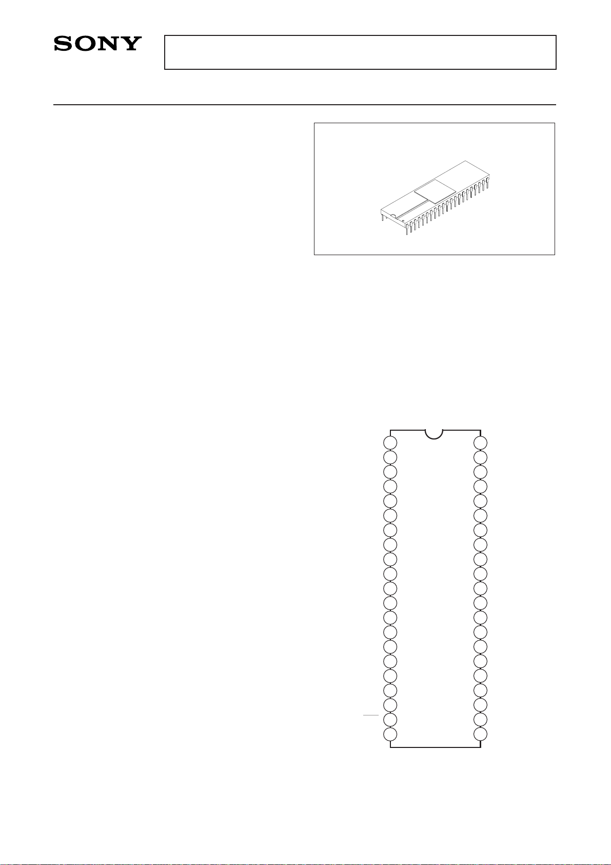
(Top View)
Description
The CXA1396D are 8-bit ultrahigh-speed flash A/D
converter ICs capable of digitizing analog signals at
the maximum rate of 125 MSPS. The digital I/O
levels of these A/D converters are compatible with
the ECL 100K/10KH/10K.
The CXA1396D is pin-compatible with the earlier
model CX20116. They can replace the earlier models
respectively, without any design changes, in most
cases. Compared with the earlier models, these new
models have been greatly improved in performance,
by incorporating advanced process, new circuit
design and carefully considered layout.
Features
• Ultrahigh-speed operation with maximum
conversion rate of 125 MSPS (Min.)
• Wide analog input bandwidth: 200MHz (Min. for
full-scale input)
• Low power consumption: 870mW (Typ.)
• Single power supply: –5.2V
• Low input capacitance
• Built-in integral linearity compensation circuit
• Low error rate
• Operable at 50% clock duty cycle
• Good temperature charactcristics
• Capable of driving 50Ω loads
Structure
Bipolar silicon monolithic IC
Applications
• Digital oscilloscopes
• HDTV (high-definition TVs)
• Other apparatus requiring ultrahigh-speed A/D
conversion
Pin Configuration
Pins without name are NC pins (not connected).
42 pin DIP (Ceramic)

– 2 –
CXA1396D
Absolute Maximum Ratings (Ta = 25°C)
• Supply voltage AVEE, DVEE –7 to +0.5 V
• Analog input voltage VIN –2.7 to +0.5 V
• Reference input voltage VRT, VRB, VRM –2.7 to +0.5 V
VRT – VRB
2.5 V
• Digital input voltage CLK, CLK, MINV, LINV –4 to +0.5 V
CLK – CLK
2.7 V
• VRM pin input curent IVRM –3 to +3 mA
• Digital output current ID0 to ID7 –30 to 0 mA
• Storage temperature Tstg –65 to +150 °C
Recommended Operating Conditions Min. Typ. Max. unit
• Supply voltage AVEE, DVEE –5.5 –5.2 –4.95 V
AVEE – DVEE –0.05 0 +0.05 V
AGND – DGND –0.05 0 +0.05 V
• Reference input voltage VRT –0.1 0 +0.1 V
VRB –2.2 –2.0 –1.8 V
• Analog input voltage VIN VRB VRT
• Pulse width of clock TPW1 4.0 ns
TPW0 4.0 ns
• Operating temperature Ta –20 +75 °C
– 3 –
CXA1396D
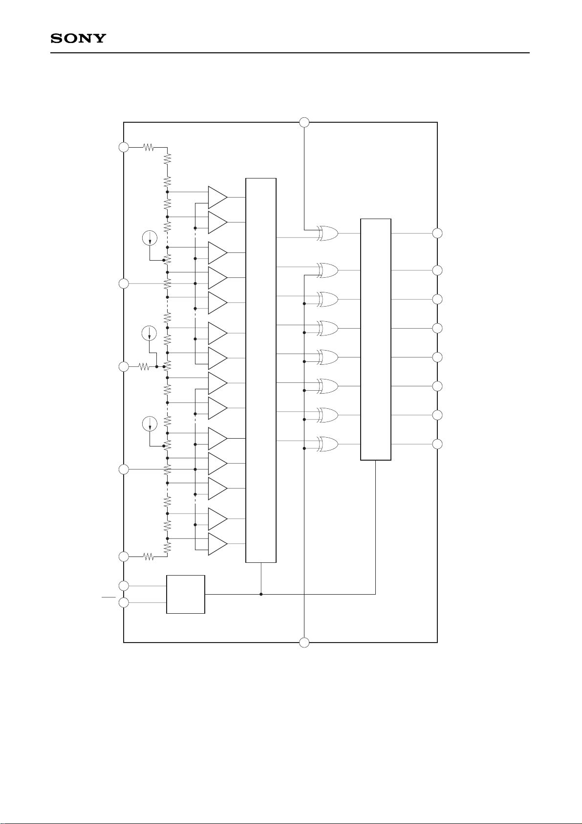
Block Diagram
255
126
127
128
129
191
192
193
254
63
64
65
1
2
CLOCK
DRIVER
•
•
•
•
•
•
•
•
•
•
•
•
r3
r1
r2
r/2
r
r
r
r
r
r
r
r
r
r
r
r
r
r
r/2
D7 (MSB)
D6
D4
D3
D5
D2
D1
D0 (LSB)
OUTPUT
ENCODE LOGIC
MINV
V
RT
VIN
VRM
VIN
VRB
CLK
CLK
LINV
Comparator
– 4 –
CXA1396D
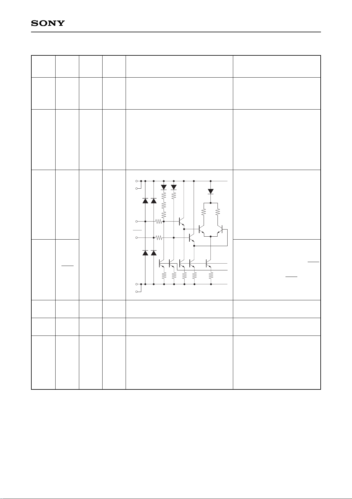
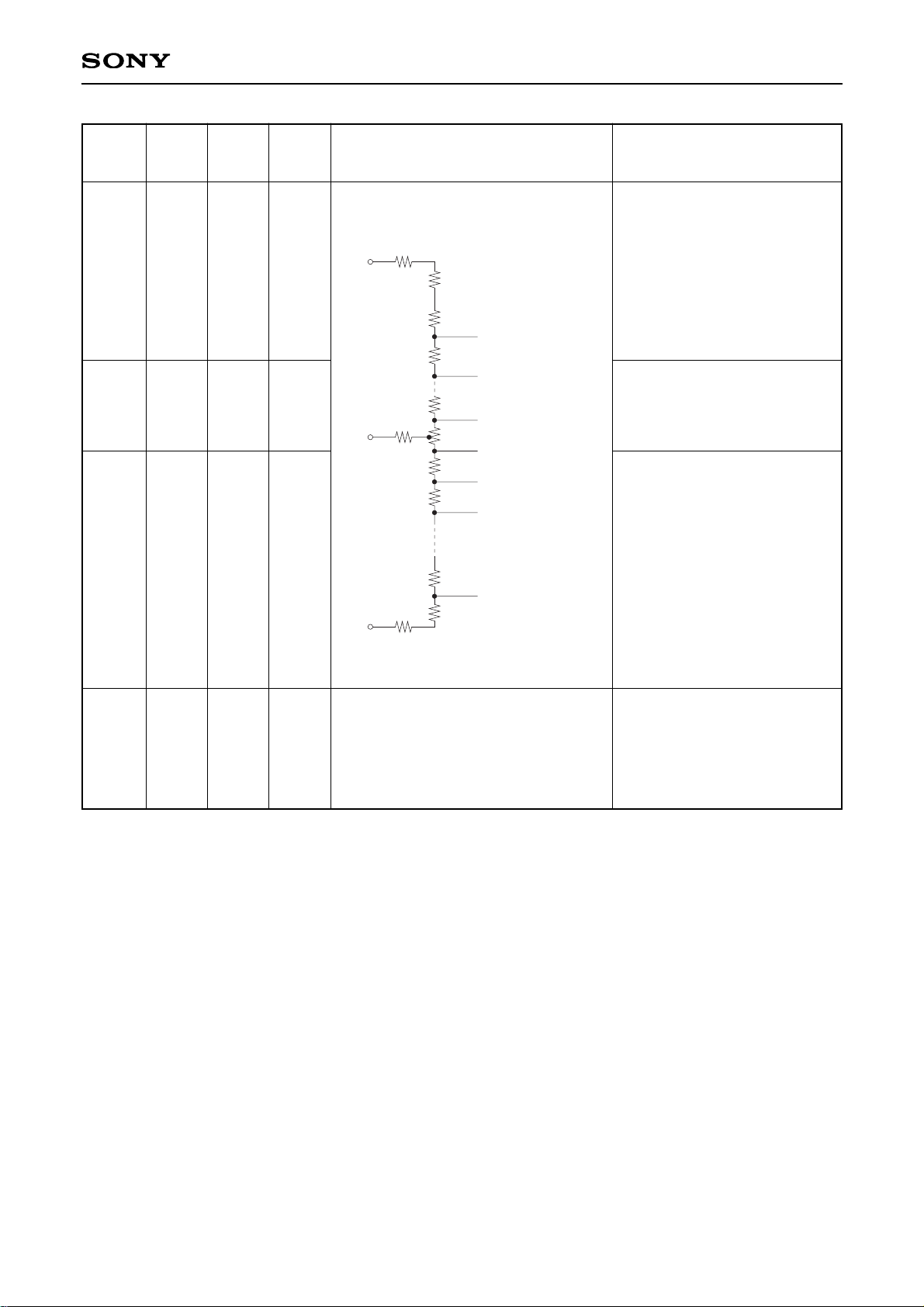
Pin Description and I/O Pin Equivalent Circuit
Analog GND.
Used as GND for input buffers
and latches of comparators.
Isolated from DGND1, DGND2.
29, 31,
33, 35
AGND — 0V
1, 25,
26, 38,
39
21
20
5, 16
6, 15 DGND2 — 0V
4, 17 DVEE — –5.2V
DGND1 — 0V
CLK
CLK
I ECL
AVEE — –5.2V
Analog VEE.
–5.2V (Typ.).
Internally connected with DVEE
(resistance: 4 to 6Ω).
A ceramic chip capacitor of at
least 0.1µF should be used to
connect to AGND and be
placed near the pins.
CLK input
Complementary input to CLK.
With open connection, kept at
threshold voltage (–1.3V).
Device is operable without CLK
input, but use of omplementary
inputs of CLK and CLK is
recommended to obtain the
stable high-speed operation.
Digital GND for internal
circuits.
Digital GND for output
transistors.
Digital VEE.
Internally connected with AVEE
(resistance: 4 to 6Ω).
A ceramic chip capacitor of at
least 0.1µF should be used to
connect to DGND near the
pins.
Pin No. Symbol I/O
Standard
voltage
level
Equivalent circuit Description
r
r
r r
r r
DGND1
CLK
CLK
DV
EE
– 5 –
CXA1396D
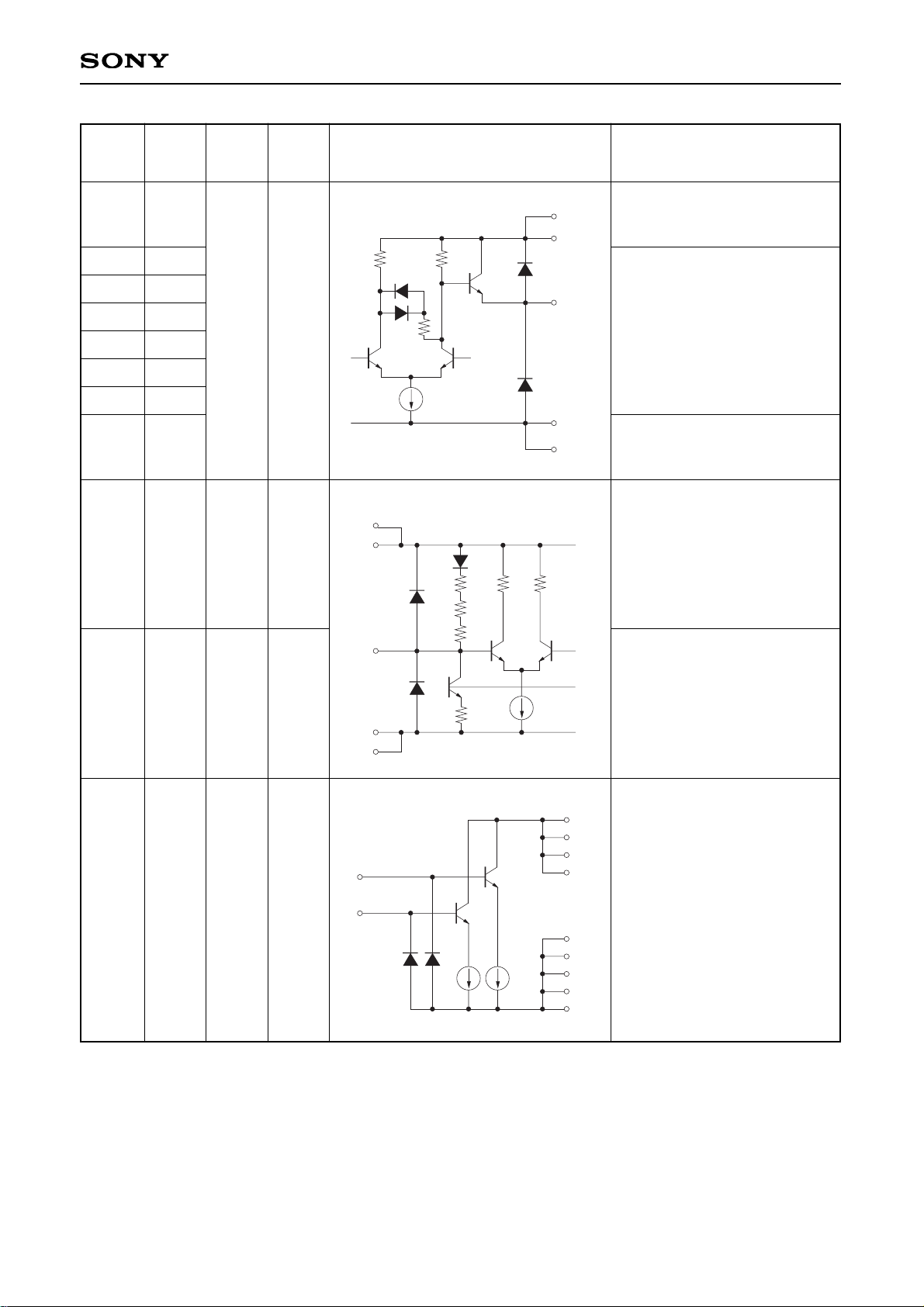
LSB of data outputs.
External pull-down resistor is
required.
Data outputs.
External pull-down resistors
are required.
MSB of data outputs.
External pull-down resistor is
required.
Input pin for D0 (LSB) to D6
output polarity inversion (see
output code table).
With open connection, kept at
"L" level.
Input pin for D7(MSB) output
polarity inversion (see output
code table).
With open connection, kept at
"L" level.
Analog input pins.
These two pins must be
connected externally, since
they are not internally
connected.
See Application Note for
precautions.
7
14
3
18
30, 34 VIN I
VRT
to
VRB
MINV I ECL
LINV I ECL
D7
8
9
10
11
12
13
D1
D2
D3
D4
D5
D6
D0
O ECL
Pin No.
Symbol I/O
Standard
voltage
level
Equivalent circuit Description
DGND2
DV
EE
Di
r
r
r
r
LINV
or
MINV
DGND1
DV
EE
–1.3V
AGND
AVEE
VIN
VIN
– 6 –
CXA1396D
Reference voltage (bottom).
Typically –2V.
A ceramic capacitor of at least
0.1µF and a tantalum capacitor
of at least 10µF should be
used to connect to AGND near
the pins.
Reference voltage mid point.
Can be used as a pin for
integral linearity compensation.
Reference voltage (top).
Typically 0V.
When a voltage except for
AGND is applied to this pin, a
ceramic capacitor of at least
0.1µF and a tantalum capacitor
of at least 10µF should be used
to connect to AGND near the
pins.
Unused pins.
No internal connections have
been made to these pins.
Connecting them to AGND or
DGND on PC board is
recommended.
23
32
41
2, 19,
22, 24,
27, 28,
36, 37,
40, 42
NC — —
VRT
I
0V
VRM I VRB/2
VRB I –2V
Pin No. Symbol I/O
Standard
voltage
level
Equivalent circuit Description
.
.
.
Comparator 1
Comparator
2
Comparator 127
Comparator 128
Comparator 129
Comparator 130
Comparator 255
.
.
.
.
.
.
.
r/2
r
r
r
r
r
r
r
r/2
r
3
r2
r1
VRT
VRM
VRB
– 7 –
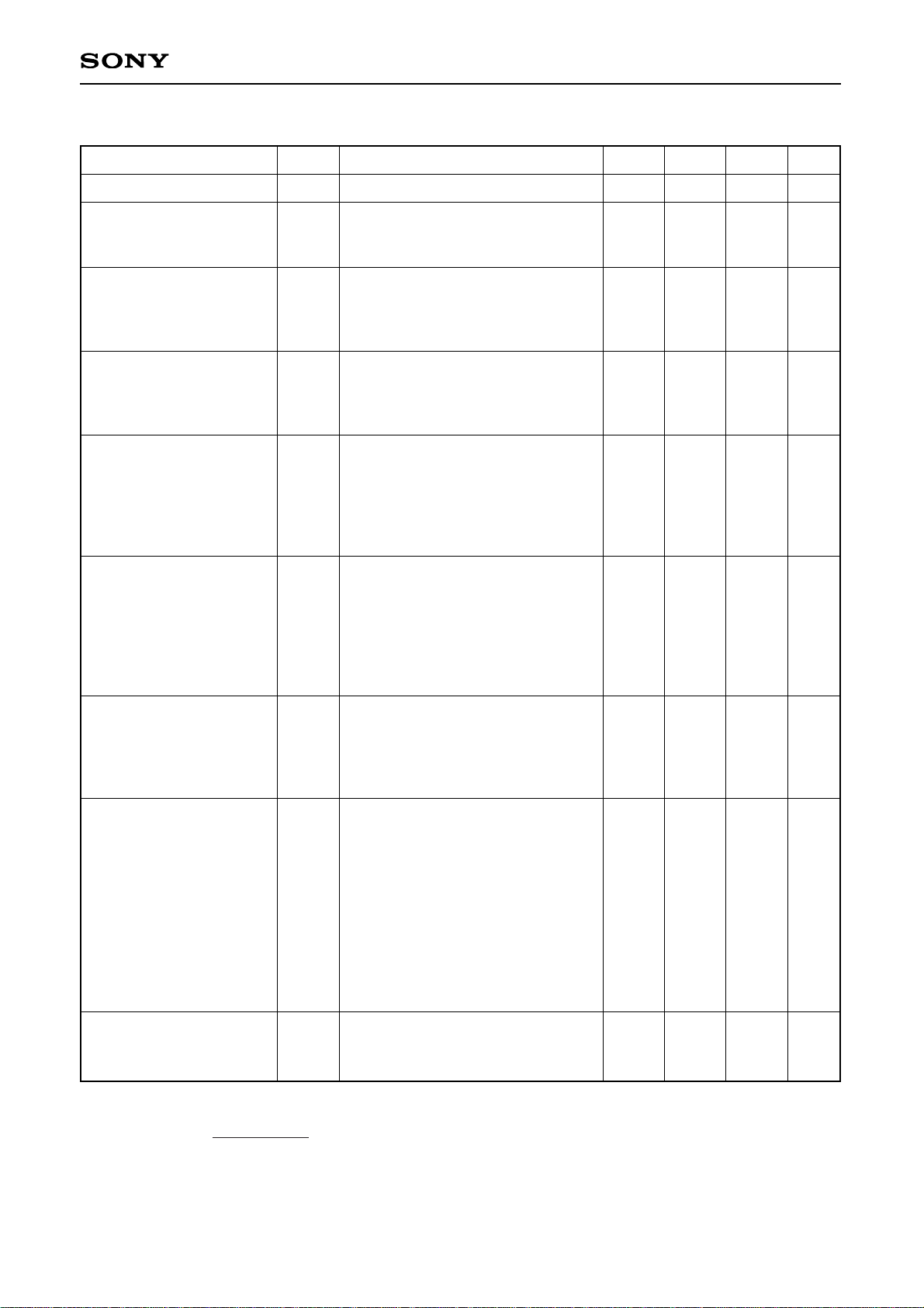
CXA1396D
Electrical Characteristics (Ta = 25°C, AVEE = DVEE = –5.2V, VRT = 0V, VRB = –2V)
Item
Resolution
DC characteristics
Integral linearity error
Differential linearity error
Analog input
Analog input capacitance
Analog input resistance
Input bias current
Reference inputs
Reference resistance
Offset voltage VRT
VRB
Digital inputs
Logic H level
Logic L level
Logic H current
Logic L current
Input capacitance
Switching characteristics
Maximum conversion rate
Aperture jitter
Sampling delay
Output delay
H pulse width of clock
L pulse width of clock
Digital outputs
Logic H level
Logic L level
Output rising time
Output falling time
Dynamic characteristics
Input bandwidth
S/N ratio
Error rate
Differential gain error
Differential phase error
Power supply
Supply current
Power consumption
∗2
n
EIL
EDL
CIN
RIN
IIN
RREF
EOT
EOB
VIH
VIL
IIH
IIL
Fc
Taj
Tds
Tdo
TPW1
TPW0
VOH
VOL
Tr
Tf
DG
DP
IEE
Pd
Fc = 125MSPS
Fc = 125MSPS
VIN = –1V + 0.07Vrms
VIN = –1V
Input connected to –0.8V
Input connected to –1.6V
Error rate 10–9TPS
∗1
RL = 50Ω to –2V
RL = 50Ω to –2V
RL = 50Ω to –2V, 20% to 80%
RL = 50Ω to –2V, 80% to 20%
VIN = 2Vp-p, 3dB down
Input = 1MHz, FS
Clock = 125MHz
Input = 31.5MHz, FS
Clock = 125MHz
Input = 31.249MHz, FS
Error > 16LSB
Clock = 125MHz
NTSC 40IRE mod.ramp,
Fc = 125MSPS
75
8
0
–1.13
0
–50
125
3.0
4.0
4.0
–1.10
200
–230
8
±0.3
±0.3
17
190
130
110
19
15
7
10
1.5
3.6
0.8
1.0
46
40
1.0
0.5
–160
870
±0.5
±0.5
320
155
32
24
–1.50
50
50
4.2
–1.62
10
–9
bits
LSB
LSB
pF
kΩ
µA
Ω
mV
mV
V
V
µA
µA
pF
MSPS
ps
ns
ns
ns
ns
V
V
ns
ns
MHz
dB
dB
TPS
∗1
%
deg
mA
mW
Symbol Condition Min. Typ. Max. Unit
{
{
}
{
∗1
TPS: times Per Sample
∗2
Pd = IEE•VEE +
RREF
(VRT – VRB)
2
 Loading...