Sony CXA1391R, CXA1391Q Datasheet
CXA1391Q/R
Processing IC for Complementary Color Mosaic CCD Camera
Description
The CXA1391Q/R is a bipolar IC developed for
signal processing in complementary color mosaic
CCD cameras.
Features
• Low power consumption (170mW)
• Number of delay lines used for signal processing
can be selected according to the system
requirements
• The LPF peripheral to 1H delay line is built in
Structure
Bipolar silicon monolithic IC
Applications
Complementary color mosaic CCD cameras
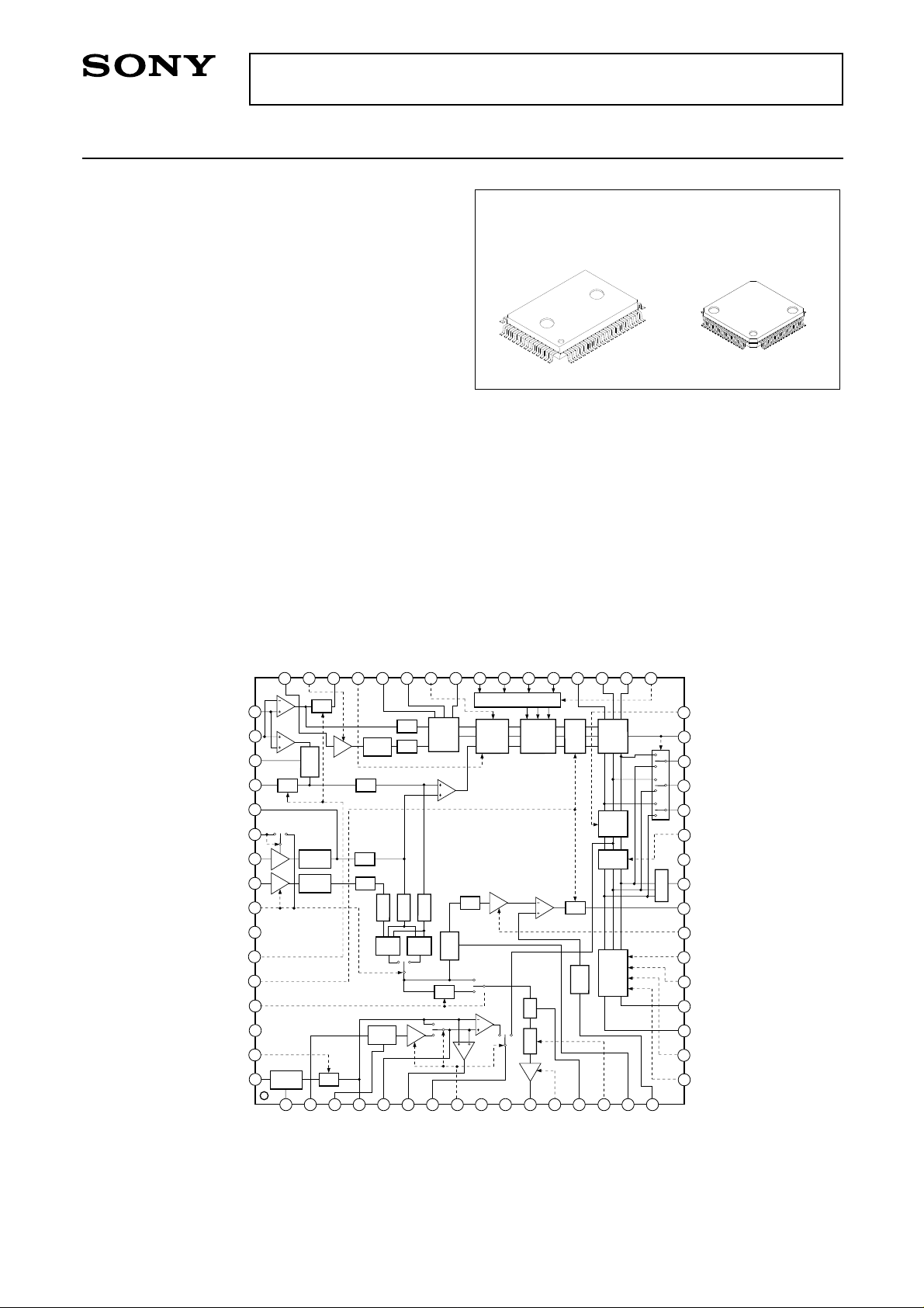
Block Diagram and Pin Configuration
(Top View)
CXA1391Q
64 pin QFP (Plastic)
CXA1391R
64 pin LQFP (Plastic)
Absolute Maximum Ratings
• Supply voltage Vcc 7 V
• Storage temperature Tstg –55 to +150 °C
• Allowable power dissipation
PD 690 mW
(LQFP: Ta = 25°C, without P.C.B)
Recommended Operating Conditions
• Supply voltage Vcc 4.75 to 5.25 V
• Ambient temperature Topr –20 to +75 °C
C LEVEL
CLF C R
CLP C G
CLP C B
R GAIN
R CONT
B CONT
B GAIN
ID
B MTX
CLP C MPX2
CLP C MPX1
R MTX
DLCO OUT
C1 GAIN
S2 IN
S1 IN
CLP C Y O
DLY0 OUT
DLY1 OUT
Y1 GAIN
DLY1 IN
DLY2 IN
Y2 GAIN
GND 2
LPF ADJ 1
LPF ADJ 2
LPF ADJ 3
VCC
Y-r CONT
YH IN
DLC1 IN
46
CLP
CLP
CLP
2
(CLP4)
Y0
DLYH IN
LPF
45
GC
Y1
Y2
YH1
YH0
r
3
CLP C DLYH
48
47
LPF
GC
GC
CLP
(CLP2)
C0
Y0
(CLP4)
(CLP4)
1
CLP C Y H
49
50
51
52
53
54
55
56
57
58
59
60
61
62
63
64
LPF
LPF
LPF
4
CLP
(CLP4)
(CLP4)
DLYH OUT
44
–
3H
APCN
CLP
5
43
C0
LPF
C1
LPF
Y0
Y1
Y1
Y0
Y2
KNEE
KNEE
KNEE
–
–
2H
APCN
V-APCN
YH0
GC
YH1
6
YH OUT 2
YH OUT 1
CLP
(CLP2)
&
MPX
LPF
7
TP
40
-CB
ABS
(CLP4)
8
DLYH GAIN
CR
Y
39
WB CONTROL
MATRIX
GC
9
10
CLP4
4142
V-APCN
CLP
B
G
WB AMP
R
CS VAP
CS-Y
V-APCN
G ch SLICE
CLP2
37
38
MAX
CLP
SLICE
GC
12
11
VAP OUT
35
36
LPF
LPF
CS
CLP
(CLP4)
CS-Y
13
14 15
VAP GAIN
CLP C VAP
CLP
(CLP2)
R-WB
G-WB
SLICE
r
R-r
G-r
MTX
R-Y
B-Y
VAP SLICE
33
34
32
C SLICE
WB DC
31
WB B
B-WB
B-r
Hue & GC
B-Y
R-Y
CLP C CS
30
B-r
WB G
29
G-r
WB R
28
R-r
C-r CONT
27
GND 1
26
YL OUT
25
YL MTX
CS OUT
24
CS GAIN
23
R – Y HUE
22
B – Y HUE
21
R – Y OUT
20
B – Y OUT
19
B – Y GAIN
18
R – Y GAIN
17
16
CS IN
Sony reserves the right to change products and specifications without prior notice. This information does not convey any license by
any implication or otherwise under any patents or other right. Application circuits shown, if any, are typical examples illustrating the
operation of the devices. Sony cannot assume responsibility for any problems arising out of the use of these circuits.
– 1 –
E89Z18-ST
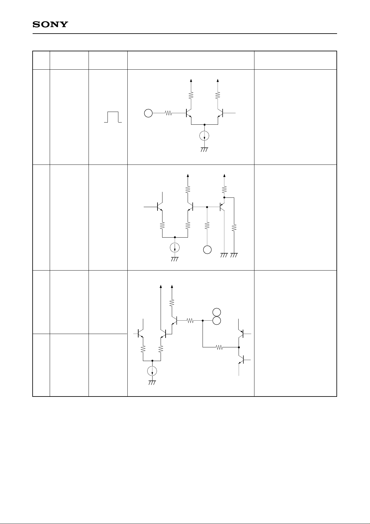
Pin Description
CXA1391Q/R
PIn
No.
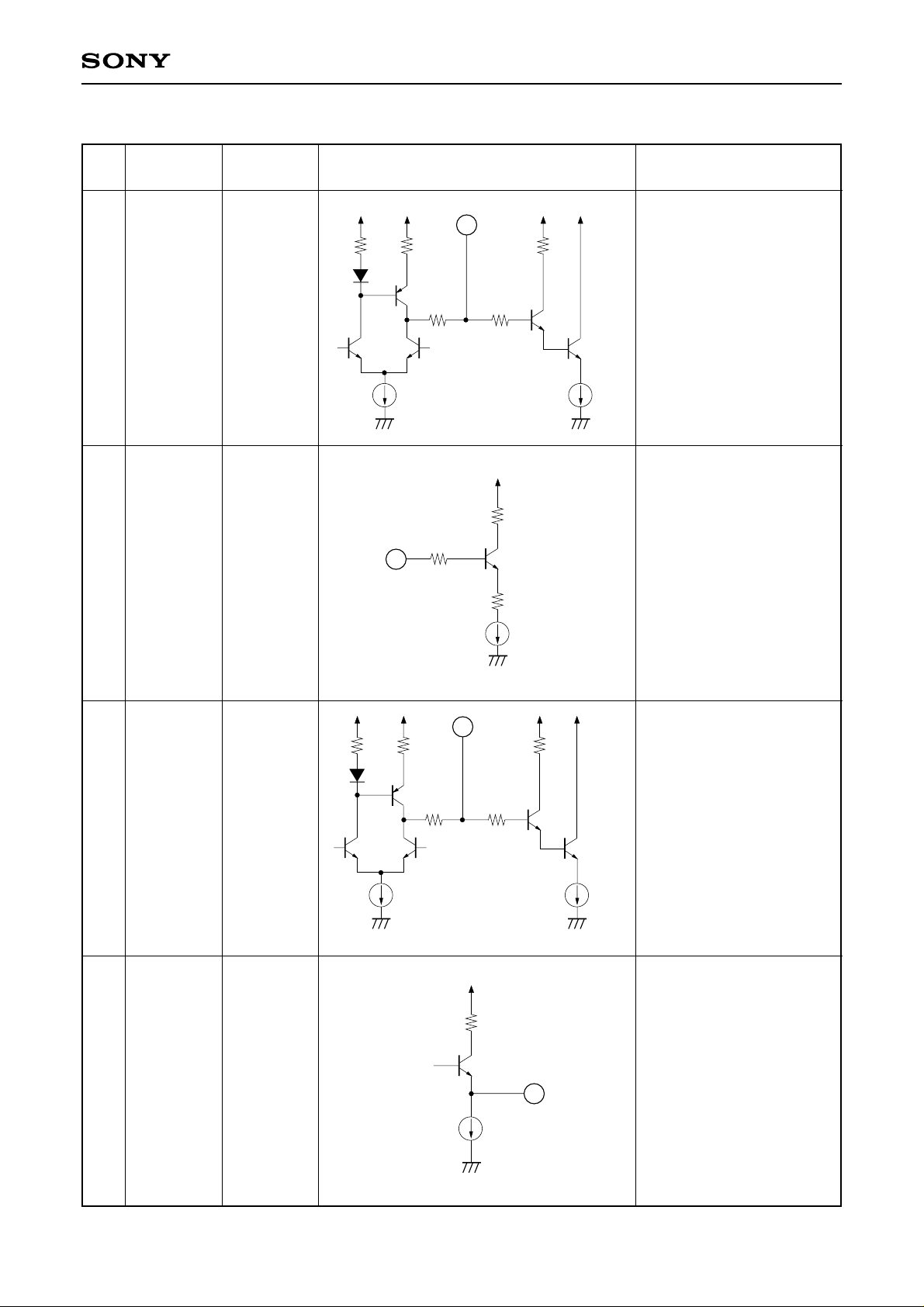
1
2
Symbol
CLP C YH
DL YH IN
Pin voltage
3 to 3.5V
3.65V
2.4k 2.4k
Equivalent circuit Description
1
800
1k 147
Capacitor connecting pin
for YH clamp
(Clamp at CLP2)
180µA 80µA
1k
147
2
5k
80µA
DL YH signal input pin
(Input from 1H delay line)
Sig: Typ. 200mV
(Positive polarity)
3
200
1k
Capacitor connecting pin
for DL YH clamp
(Clamp at CLP4)
40µA
DL YH signal output pin
2.6k 2.6k
CLP C
3
DL YH
2.6 to 3.8V
1k 147
180µA
(To 1H delay line)
DL YH
4
OUT
2.7 to 3.1V
4
Sig: Typ. 400mV
Max. 600mV
400µA
(Negative polarity)
Note) Pin voltage for input and output pins indicate black level.
– 2 –
CXA1391Q/R
PIn
No.
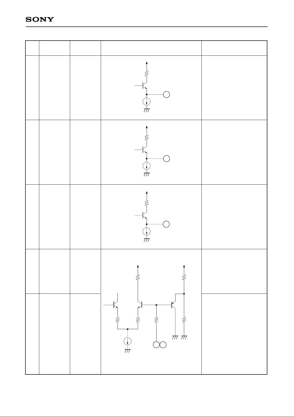
5
6
Symbol Pin voltage Equivalent circuit Description
YH OUT1
YH OUT2
100
1.9 to 2.3V
5
160µA
100
1.9 to 2.3V
6
400µA
YH1 signal output pin
Sig: Typ. 1V
Max. 1.5V
(Positive polarity)
YH2 signal output pin
Sig: Typ. 1V
Max. 1.5V
(Positive polarity)
7
8
54
TP
DL YH GAIN
Y1 GAIN
2.6 to 3.0V
(YH)
2.5 to 2.9V
(G)
0V
(0H Mode)
1.8 to 5V
(1H Mode)
0V:
Common
control by
Pin 57
1.8 to 5V
Independent
control
30k
500
7
80µA
1k
30k 147 100k
40µA
8
54
100k
TP OUT (adjusting pin)
1H mode: Outputs YH1–YH0
0H mode: Outputs Gch
C-slice OUT
(Mode selection is executed
through Pin 8)
DL YH signal gain control
pin
(For 1H delay line gain
compensation of YH)
TP (Pin 7) mode selection
0H Mode: 0V
1H Mode: 1.8 to 5V
DLY1 signal gain control pin
(1H delay line gain
compensation)
0V: DLY1 signal gain
control is executed in
common with DLY2
signal gain control.
1.8 to 5V: DLY1 signal gain
control is executed
independently from
DLY2 signal gain
control.
– 3 –
CXA1391Q/R
PIn
No.
9
10
11
Symbol Pin voltage Equivalent circuit Description
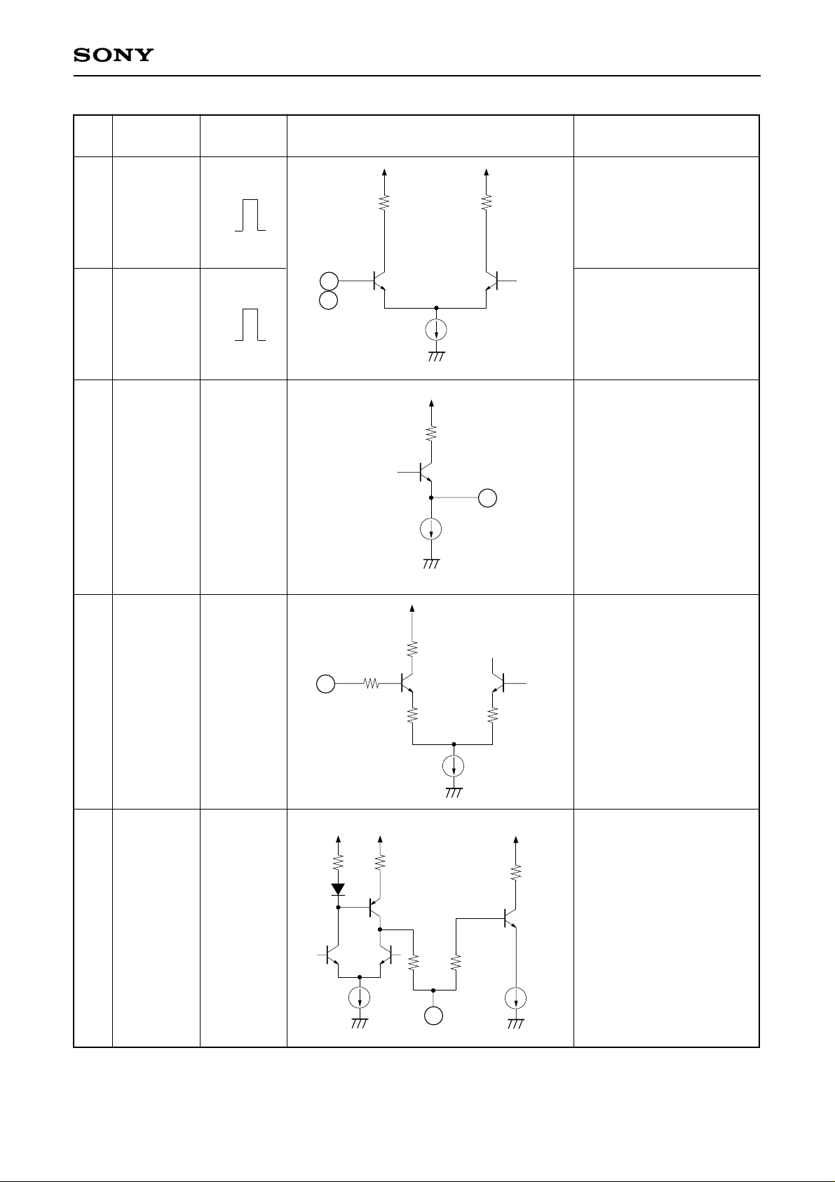
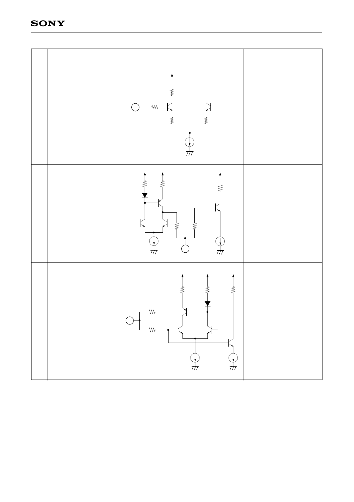
CLP4 pulse input pin
CLP4
CLP2
5V
0
5V
0
9
10
40µA
431
30k1k
(BLK clamp)
(CMOS level input,
VTH = 2.5V)
CLP2 pulse input pin
(OPB clamp)
(CMOS level input,
VTH = 2.5V)
V-APCN signal output pin
VAP OUT
2.6 to 3.0V
280µA
11
Sig: Max. 1.2Vp-p
∗
12
13
VAP GAIN
CLP C VAP
1.8 to 5V
(Control)
3.4 to 3.8V
1k
147
12
25k
2.6k 2.6k
147
180µA
13
40µA
147
25k
V-APCN signal output level
adjustment pin
1k
Capacitor connecting pin
for VAP clamp
(Clamp at CLP4)
12µA
∗
V-APCN: Vertical Aperture Compensation
– 4 –
CXA1391Q/R
PIn
No.
14
15
Symbol Pin voltage Equivalent circuit Description
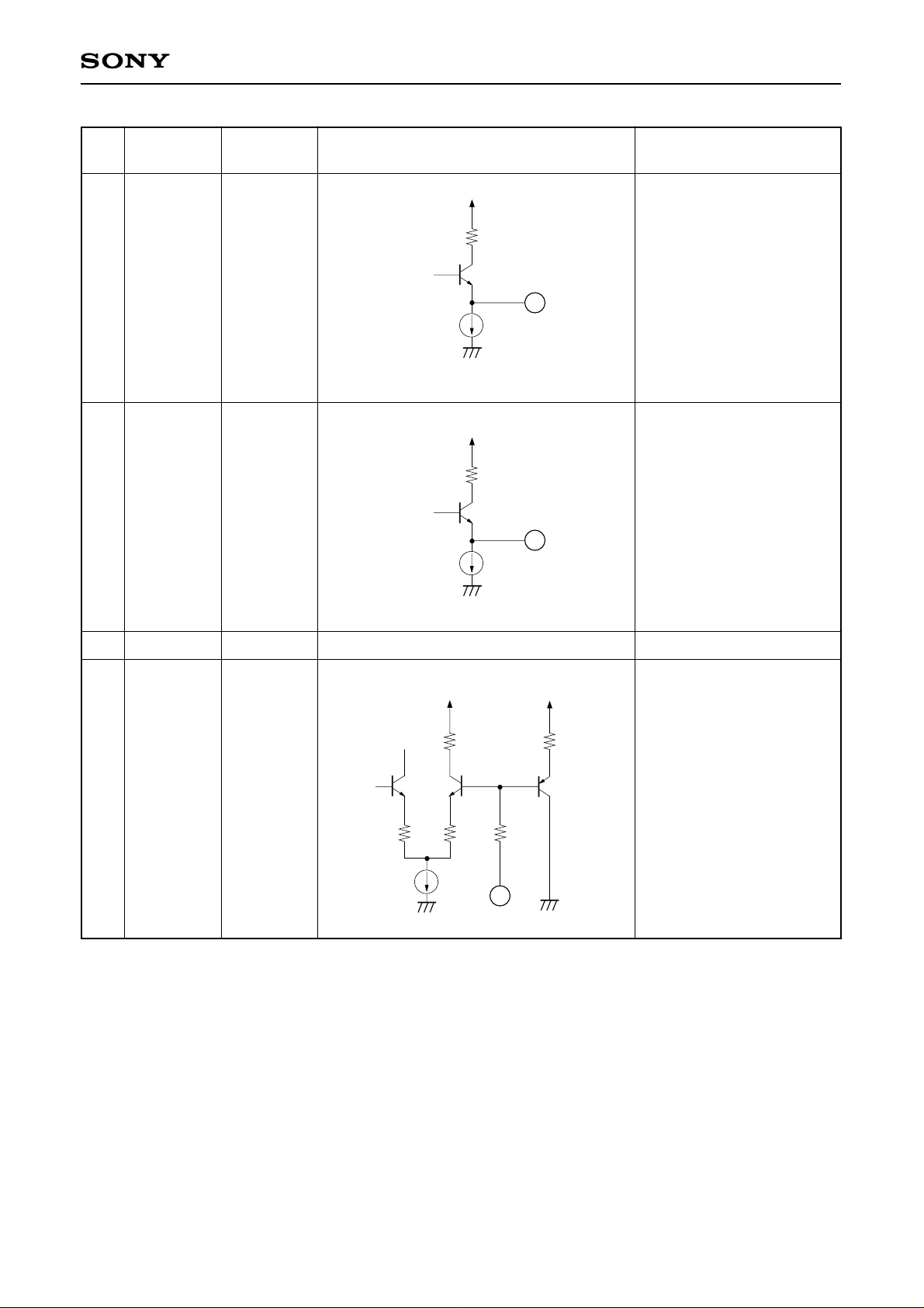
1k
147
VAP SLICE
1.8 to 5V
(Control)
14
2.6k
30k
2.6k
30k
40µA
1k
V-APCN signal
dark slice volume
adjustment pin
Capacitor connecting pin
CLP C CS
3.5 to 3.7V
for CS clamp
(Clamp at CLP4)
147
147
180µA
15
20µA
16
CS IN
C-Couple
input
2.9 to 3.3V
16
147
147
2.6k 2.6k
1k
AGC CS signal input pin
Sig: Max. 1V
20µA180µA
– 5 –

CXA1391Q/R
17
18
23
19
20
46
R–Y GAIN
B–Y GAIN
CS GAIN
B–Y OUT
R–Y OUT
DLC0 OUT
0V:
R–G output
1.8 to 5V:
R–Y output
0V:
B–G output
1.8 to 5V:
B–Y output
1.8 to 5V
(Control)
2.75 to 3.15V
(Hue OFF)
2.35 to 2.75V
(Hue ON)
1.8 to 2.2V
R–Y signal output level
adjustment pin
Pin 20 Mode select
0V: R–G output
1.8 to 5V: R–Y output
B–Y signal output level
adjustment pin
Pin 19 Mode select
0V: B–G output
1.8 to 5V: B–Y output
V-APCN CS signal
gain control pin
52
53
21
DLY0 OUT
DLY1 OUT
B–Y Hue
1.4 to 1.8V
2.8 to 3.2V
0V:
B–Y hue control pin
R–Y hue control pin
– 6 –
CXA1391Q/R
PIn
No.
24
25
Symbol Pin voltage Equivalent circuit Description
431
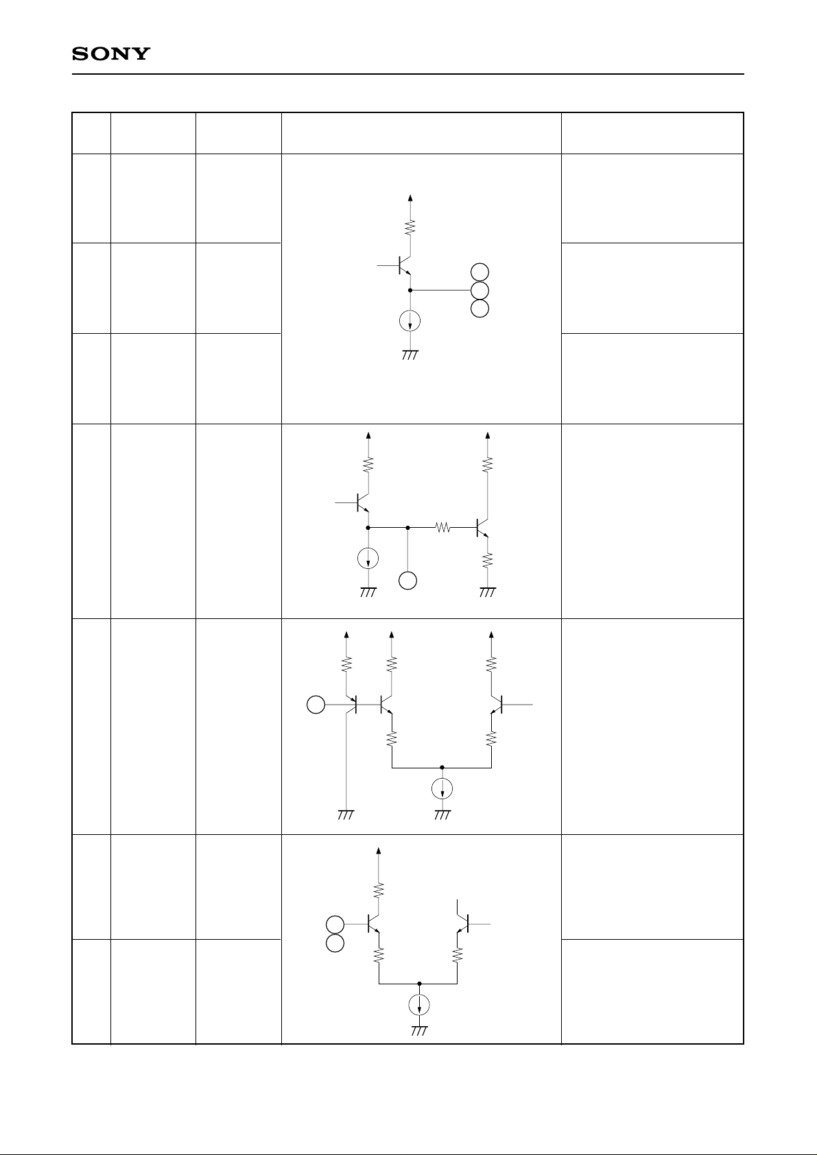
CS signal output pin
CS OUT
YL OUT
1.5 to 1.8V
1.9 to 2.3V
200µA
431
80µA
25
24
Sig: Max. 1V
YL signal output pin
26 GND1
C-γ CONT
27
0V: Typ.
γ curve
30k
40µA
1k
30k
GND
100k
Chroma (R.G.B)
γ curve adjustment pin
147
27
– 7 –
CXA1391Q/R
PIn
No.
28
29
30
31
Symbol Pin voltage Equivalent circuit Description
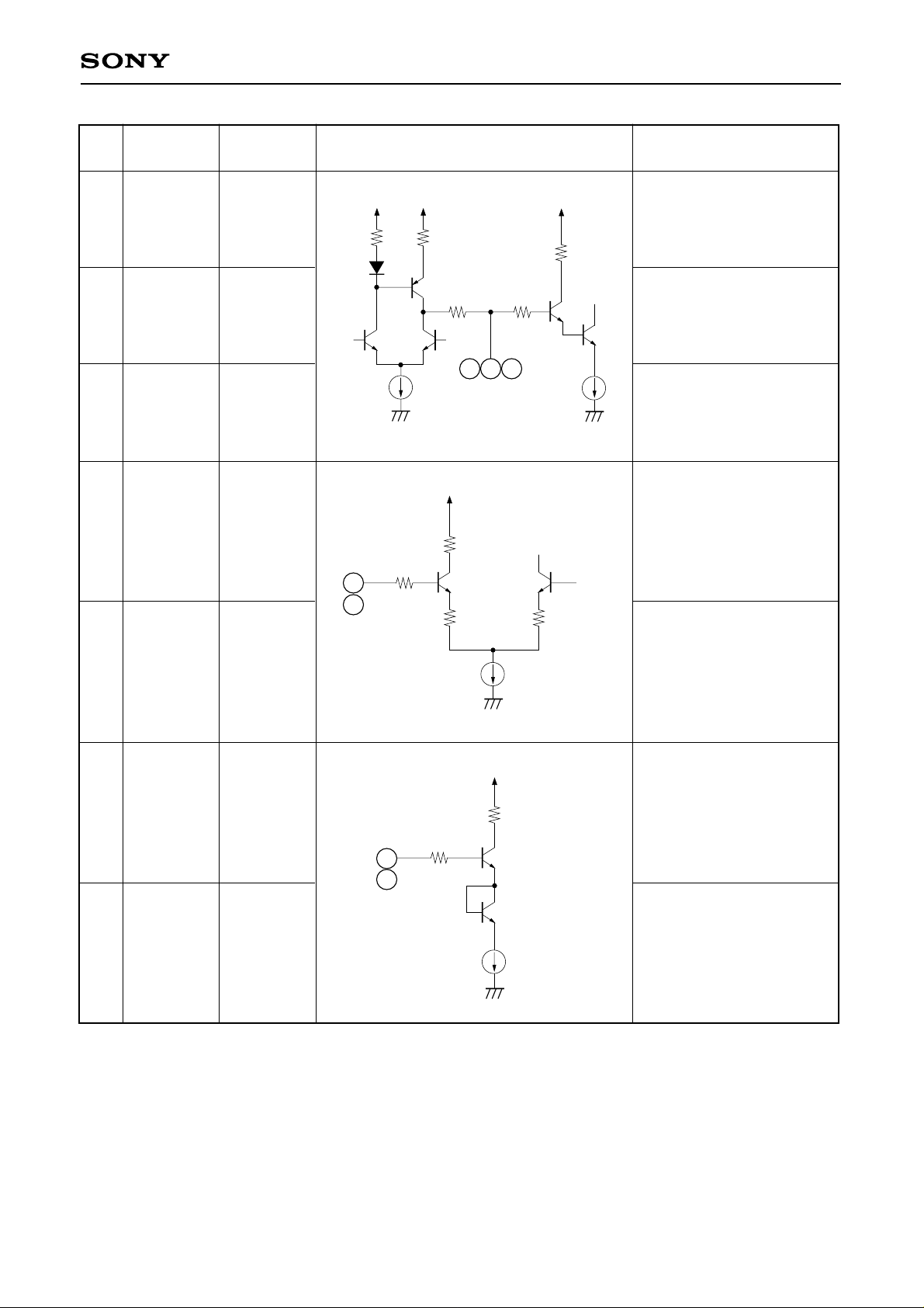
R signal output pin
WB Mode:
WB R
1.4 to 2V
Sig: Typ. 400mV
γ Mode:
431
Sig: Typ. 500mV
G signal output pin
WB G
1.4 to 2V
28
29
30
200µA
WB Mode:
Sig: Typ. 400mV
γ Mode:
Sig: Typ. 500mV
B signal output pin
WB Mode:
WB B
1.4 to 2V
Sig: Typ. 400mV
γ Mode:
Sig: Typ. 500mV
431 1k
When used as output pin,
it is an Auto WB DC output
pin.
Pin 28, 29 and 30 turn
to WB mode.
WB DC
1.4 to 2V
300
32
C SLICE
33
C LEVEL
47 C1 GAIN
0V:
Slice OFF
1.8 to 5V
(Control)
1.8 to 5V
(Control)
100k
32
200µA
33
47
30k
18k
1k
31
1k
40µA
67µA
30k
100k
18k
When connected to Vcc:
Pins 28, 29 and 30 turn to
γ mode.
Chroma (R.G.B) signals
dark slice level adjustment
pin
Chroma (R.G.B) gain
control pin
(Chroma modulation factor
control for all 3 channels)
DL C1 signal gain control
pin
(1H delay line gain
compensation)
– 8 –
CXA1391Q/R
PIn
No.
34
35
36
37
Symbol Pin voltage Equivalent circuit Description
Capacitor connecting pin
CLP C R
CLP C G
3.0 to 3.6V
3.0 to 3.6V
2.2k 2.2k
1k
147
for R WB amplifier clamp
(Clamp at CLP2)
1k
Capacitor connecting pin
for G WB amplifier clamp
(Clamp at CLP2)
35
36
34
CLP C B
125µA
3.0 to 3.6V
40µA
Capacitor connecting pin
for B WB amplifier clamp
(Clamp at CLP2)
Rch WB amplifier gain
control pin
(Pre-WB)
R GAIN
1.8 to 5V
(Control)
37
40
147
15k
1k
15k
40
38
39
B GAIN
R CONT
B CONT
1.8 to 5V
(Control)
2.5 to 4.6V
2.5 to 4.6V
38
39
147
80µA
1k
10µA
Bch WB amplifier gain
control pin
(Pre-WB)
Rch WB amplifier gain
control pin
Bch WB amplifier gain
control pin
– 9 –
CXA1391Q/R
PIn
No.
41
42
Symbol Pin voltage Equivalent circuit Description
ID pulse
(color discrimination pulse)
input pin
(CMOS level VIH = 2.5V)
ID = L C0 → CR
ID
5V
0
41
147
1k
30k
C1 → CB
40µA
ID = H C0 → CB
C1 → CR
B MTX
1.8 to 5V
(Control)
0V
(Preset)
15k
1k
15k 147
100k
100k
B signal operations MTX
coefficient adjustment pin
(Coefficient 0.22)
Refer to Note 2.
43
44
CLP C
MPX2
CLP C
MPX1
2.7 to 3.1V
2.7 to 3.1V
6k
6k
40µA
1k
80µA
147
42
43
44
147
Capacitor connecting pin
for MPX clamp
(Clamp at CLP2)
– 10 –
 Loading...