

Sony CXA1372BS, CXA1372BQ Datasheet

CXA1372BQ/BS
RF Signal Processing Servo Amplifier for CD Player
Description
The CXA1372BQ/BS is a bipolar IC developed for
RF signal processing (focus OK, mirror, defect
detection, EFM comparator) and various servo
control.
Features
• Dual ±5V and single 5V power supplies
• Low power consumption
• Fewer external parts
• Disc defect countermeasure circuit
• Fully compatible with the CXA1182 for microcomputer
software
Functions
• Auto asymmetry control
• Focus OK detection circuit
• Mirror detection circuit
• Defect detection, countermeasure circuit
• EFM comparator
• Focus servo control
• Tracking servo control
• Sled servo control
CXA1372BQ
48 pin QFP (Plastic)
Absolute Maximum Ratings (Ta = 25°C)
• Supply voltage VCC – VEE 12 V
• Operating temperature
Topr –20 to +75 °C
• Storage temperature
Tstg –65 to +150 °C
• Allowable power dissipation
PD 457 (CXA1372BQ) mW
833 (CXA1372BS) mW
Recommended Operating Conditions
VCC – VEE 3.6 to 11 V
VCC – DGND 3.6 to 5.5 V
CXA1372BS
48 pin SDIP (Plastic)
Structure
Bipolar silicon monolithic IC
Sony reserves the right to change products and specifications without prior notice. This information does not convey any license by
any implication or otherwise under any patents or other right. Application circuits shown, if any, are typical examples illustrating the
operation of the devices. Sony cannot assume responsibility for any problems arising out of the use of these circuits.
– 1 –
E95927A67-PS
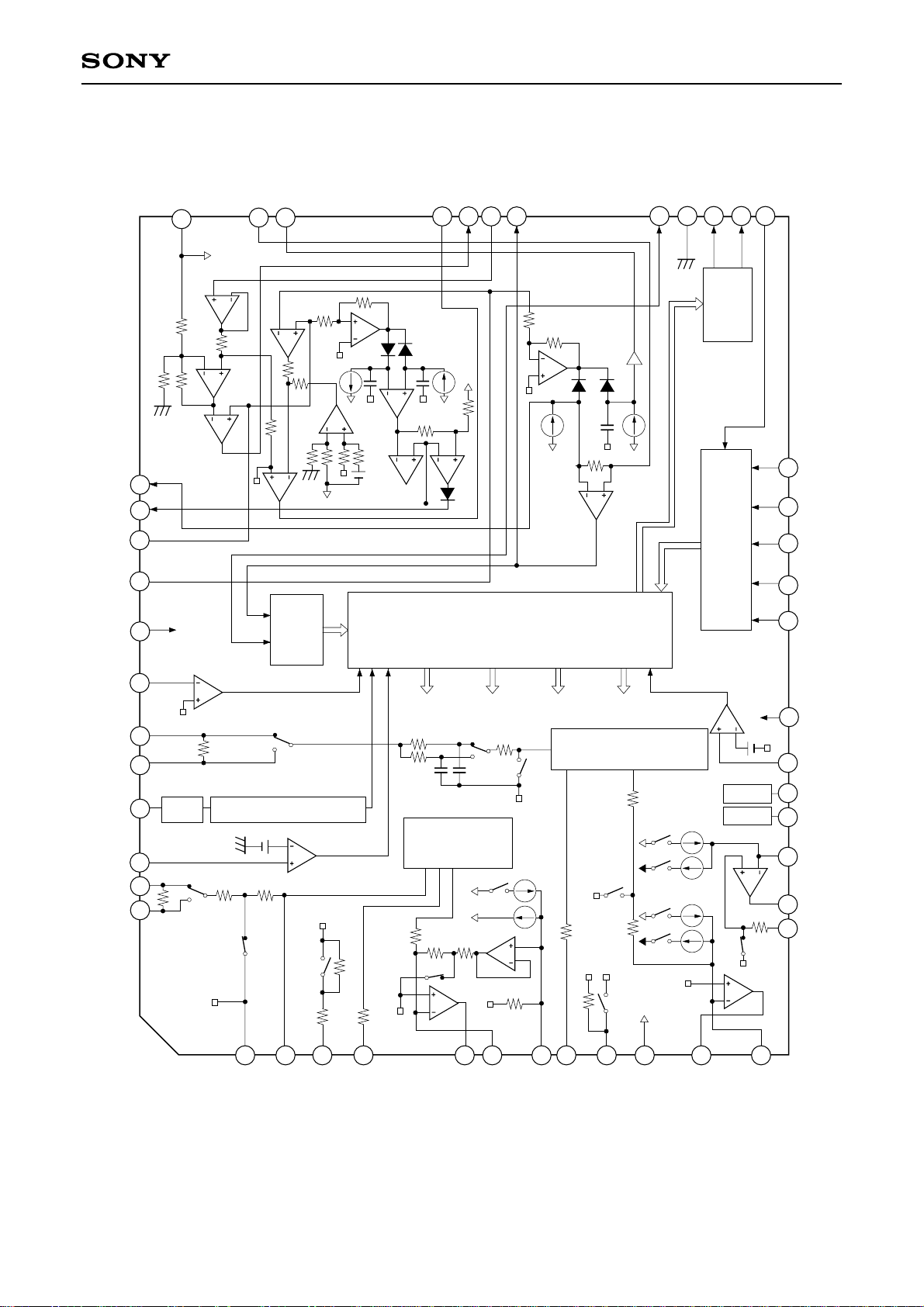
Block Diagram
36
37
CB
CP
38
39
RFI
DVcc
35
CC2
34
CC1
33
FOK
32
EFM
31
ASY
30
DFCT
29
MIRR
DGND
28
SENS
27
• IIL
• TTL
• TTL
• IIL
C. OUT
26
↓
↓
CXA1372BQ/BS
XRST
25
DATA
24
XLT
23
CLK
22
RFO
DV
TZC
TE
TDFCT
ATSC
FZC
FE
FDFCT
40
• TTL
41
EE
↓
• IIL
• IIL DATA REGISTER
• OUTPUT DECODER
• INPUT SHIFT REGISTER
• ADDRESS DECODER
21
20
LOCK
DIRC
42
• FS1 to 4 • TG1 to 2 • TM1 to 7 • PS1 to 3
AV
EE
TM2
19
18
17
16
15
14
13
SSTOP
ISET
FSET
SL–
SLO
SL+
44
45
46
47
48
43
• BPF
DFCT
• WINDOW COMPARATOR
DFCT
FS4
FS3
TG1
TM1
• FOCUS
PHASE
COMPENSATION
FS1
FS2
• TRACKING
PHASE COMPENSATION
TM6
TM5
TM7
TM4
TM3
• I SET
• F SET
TG2
6
1
2
VC
FGD
3
FS3
4
FLB
5
FEO
FE–
7
SRCH
8
TGU
9
TG2
10
CC
AV
11
TAO
12
TA–
– 2 –
Pin Configuration
CXA1372BQ
CXA1372BQ/BS
CB
CP
RFI
RFO
DV
EE
TZC
TE
TDFCT
ATSC
FZC
FE
FDFCT
37
38
39
40
41
42
43
44
45
46
47
48
36
DVcc
1
VC
35
CC2
2
FGD
34
CC1
3
FS3
FOK
33
4
FLB
ASY
EFM
32
31
CXA1372BQ
6
5
FE–
FEO
DFCT
30
7
SRCH
29
8
MIRR
TGU
DGND
28
9
TG2
27
10
SENS
11
AVcc
C. OUT
26
TAO
25
12
XRST
24
23
22
21
20
19
18
17
16
15
14
13
TA–
DATA
XLT
CLK
LOCK
DIRC
EE
AV
SSTOP
ISET
FSET
SL–
SLO
SL+
CXA1372BS
TZC
48
47
1
2
TE
EE
DV
46
3
TDFCT
RFO
45
4
ATSC
RFI
TZC
44
EE
XLT
40
9
CC1
FS3
10
FOK
39
FLB
EFM
37
38
CXA1372BS
12
11
FEO
ASY
FE–
36
13
DFCT
35
14 15
SRCH
MIRR
34
TGU
DGND
33
16
TG2
SENS
32
17
AVcc
C. OUT
TAO
CP
CB
43
6
5
FE
FDFCT
42
7
DVcc
VC
CC2
41
8
FGD
31
18
XRST
30
19
TA–
DATA
29
20
SL+
SLO
28
21
CLK
SL–
27
22
LOCK
26
23
FSET
DIRC
ISET
AV
25
24
SSTOP
– 3 –
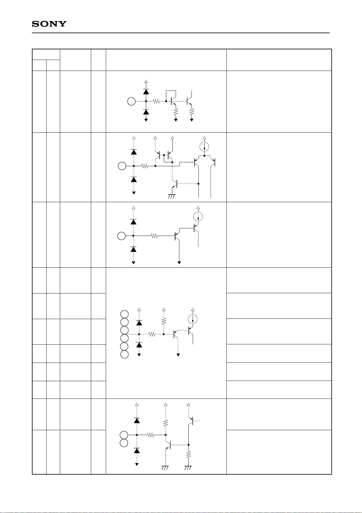
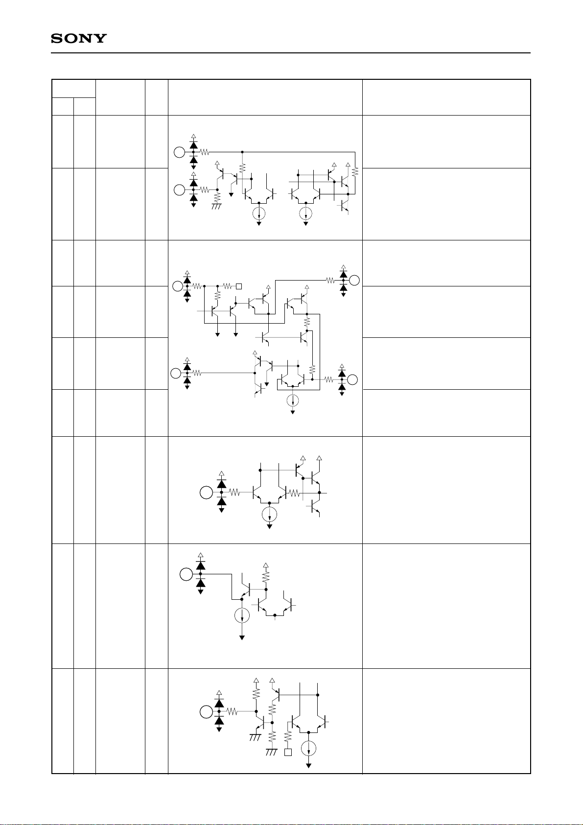
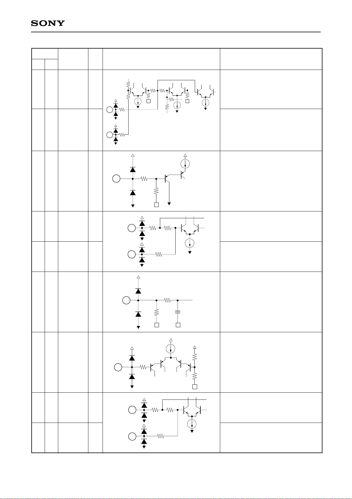
Pin Description
CXA1372BQ/BS
Pin No.
S
Q
1
2
3
7
8
9
Symbol
VC
FGD
FS3
I/O
I
I
I
Equivalent circuit
Vcc
147
2
VEE
46k 580k
3
48k
130k
20µA
Description
Center voltage input.
For dual power supplies: GND
For single power supply:
(VCC + GND)/2
Connects a capacitor between this
pin and Pin 3 to cut high-frequency
gain.
The high-frequency gain of the
focus servo is switched through FS3
ON and OFF.
4
5
11
14
6
10
11
17
20
12
FLB
FEO
TAO
SLO
FE–
I
4
40k
O
5
O
11
14
250µA
2.5µA
O
I
6
147
90k
40k
2.5µA
External time constant to boost the
low frequency of the focus servo.
Focus drive output.
Tracking drive output.
Sled drive output.
Inverted input for focus amplifier.
– 4 –
CXA1372BQ/BS
Pin No.
QS
13
7
14
8
15
9
Symbol
SRCH
TGU
TG2
I/O
Equivalent circuit
7
I
I
I
147
50k
8
9
3.5µA
110k
20k
82k
147
470k
External time constant for forming
the focus search waveforms.
11µA
External time constant for selecting
the tracking high-frequency gain.
External time constant for selecting
the tracking high-frequency gain.
Description
12
13
15
18
19
21
TA–
SL+
SL–
13
90k
10k
3µA
3µA
Inverted input for tracking amplifier.
11µA
Non-inverted input for sled amplifier.
Inverted input for sled amplifier.
22µA
12
I
147
I
I
15
147
– 5 –
CXA1372BQ/BS
Pin No.
S
Q
22
16
17
23
24
18
Symbol
FSET
ISET
SSTOP
I/O
I
I
I
17
18
Equivalent circuit
147
16
147
147
Description
Sets the peak frequency of focus
tracking phase compensation.
15k 15k
Current is input to determine focus
search, track jump, and sled kick
level.
7µA
Limit SW ON/OFF signal detection
for disc innermost track detection.
20
21
22
23
24
25
26
27
26
27
28
29
30
31
32
33
DIRC
LOCK
CLK
XLT
DATA
XRST
C. OUT
SENS
I
Used for 1-track jump. Contains a
47kΩ pull-up resistor.
At "Low" sled overrun prevention
I
20
21
I
I
22
23
24
25
147
47k
15µA
I
I
O
20k
26
27
O
147
100k
circuit operates. Contains a 47kΩ
pull-up resistor.
Serial data transfer clock input from
CPU. (no pull-up resistor)
Latch input from CPU.
(no pull-up resistor)
Serial data input from CPU.
(no pull-up resistor)
Reset input, reset at "Low".
(no pull-up resistor)
Track number count signal output.
Outputs FZC, AS, TZC and SSTOP
through command from CPU.
– 6 –
CXA1372BQ/BS
Pin No.
QS
29
35
38
44
34
40
35
41
30
36
Symbol
MIRR
CP
CC1
CC2
DFCT
I/O
O
O
O
Equivalent circuit
Description
MIRR comparator output.
147
38
147
29
I
20k
(DC voltage: 10kΩ load connected)
Connects MIRR hold capacitor.
Non-inverted input for MIRR
comparator.
DEFECT bottom hold output.
147
37
I
147
30
147
147
35
Input for DEFECT bottom hold
output with capacitance coupled.
DEFECT comparator output.
(DC voltage: 10kΩ load connected)
34
37
31
32
43
37
38
CB
ASY
EFM
I
I
32
147
31
4.8k
O
Current source depending on
power supply
(VCC to DGND)
Connects DEFECT bottom hold
capacitor.
Auto asymmetry control input.
EFM comparator output.
(DC voltage: 10kΩ load connected)
33
FOK O
39
33
20k
147
FOK comparator output.
(DC voltage: 10kΩ load connected)
– 7 –
CXA1372BQ/BS
Pin No.
S
Q
45
39
4640
42
48
43
1
Symbol
RFI
RFO
TZC
TE
I/O
O
I
Equivalent circuit
I
40k
147
39
147
40
7µA
42
147
Input for RF summing amplifier
output with capacitance coupled.
RF summing amplifier output.
Check point of eye pattern.
Tracking zero-cross comparator
Description
input.
75k
147
I
43
470k
Tracking error input.
44
45
46
47
2
3
4
5
TDFCT
ATSC
FZC
FE
147
147
147
470k
330k
470k
47P
60k
1.2k
45
Vcc
V
44
EE
I
I
I
46
I
47
Connects a capacitor for time
constant during defect.
Window comparator input for ATSC
detection.
Focus zero-cross comparator input.
Focus error input.
48
6
FDFCT
I
48
147
Connects a capacitor for time
constant during defect.
– 8 –
Unit
Max.
mA
27
mA
–8
dB
24.0
dB
–35
CXA1372BQ/BS
V
V
V
–2.0
V
–1.2
mV
–360
mV
640
mV
61
dB
17.6
dB
–39
V
V
V
V
mV
mV
–2.0
–1.2
–360
640
19
–17
Typ.
8
Min.
CC = 2.5V, VEE = –2.5V, D. GND = –2.5V)
Description of output
waveform and measurement
(Ta = 25°C, V
method
21.0
–24
18.0
1 = 10Hz, 100mVp-p
V
GFEO = 20 log (Vout/Vin)
5
10, 36
Measure-
ment
point
19, 41
E3 E4
Bias condition
00
00
SD
08
S9 E1 E2
2.0
SG = 10kHz, 40mVp-p
Difference in gain when
SD = 00 and SD = 08
V1 = 0.5VDC
5
00
5
08
V1 = –0.5VDC
5
08
1.2
V1 = 0.5VDC
5
08
V1 = –0.5VDC
5
08
–640
5
02
50
39
360
(VCC + DGND)/2 = SENS
∗
5
27
13.3
11.6
value when E4 is varied.
V2 = 10Hz, –500mVp-p
11
∗
03
00
25
2.0
GTEO = 20 log (Vout/Vin)
V2 = 10kHz, 40mVp-p
Difference in gain when
SD = 00 and SD = 25
V2 = –0.5VDC
11
11
00
25
V2 = 0.5VDC
11
25
1.2
V2 = –0.5VDC
11
25
V2 = 0.5VDC
11
25
–640
11
2C
360
11
28
S4 S5 S6 S7 S8
SW condition
S1 S2 S3
ICC
IEE
Symbol
GFEO
Item
DC voltage gain
Current consumption
Current consumption
1
2
No.
Electrical Characteristics
3
O
O
VFEOF
Feedthrough
4
VFE01
VFE02
Max. output voltage
Max. output voltage
5
6
O O
O O
VFE03
VFE04
VSRCH1
VSRCH2
Max. output voltage
Max. output voltage
Search output voltage
Search output voltage
FOCUS SERVO
7
8
9
10
– 9 –
VFZC
GTEO
FZC threshold value
DC voltage gain
11
12
VTEOF
Feedthrough
13
O
O
O O
O O
VTE01
VTE02
VTE03
VTE04
VJUMP1
Max. output voltage
Max. output voltage
Max. output voltage
Max. output voltage
Jump output voltage
TRACKING SERVO
14
15
16
17
18
VJUMP2
Jump output voltage
19
Unit
Max.
Typ.
mV
–7
–26
mV
45
26
mV
20
0
dB
dB
–34
CXA1372BQ/BS
V
V
V
–2.0
V
–2.0
mV
–450
mV
750
mV
–10
–25
V
–2.0
V
–2.0
mV
–330
–356
V
V
kHz
–1.8
7
–45
Min.
CC + DGND)/2 = SENS
(V
Description of output
∗
waveform and measurement
method
27
Measure-
ment
point
–20
(VCC + DGND)/2 = SENS
value when E3 is varied.
∗
value when E2 is varied.
27
27
E4
∗
∗
Bias condition
10
10
SD
20
S9 E1 E2 E3
50
V5 = 10Hz, 20mVp-p
Open loop gain
V5 = 10kHz, 100mVp-p
Difference in gain when
SD = 00 and SD = 25
14
25
14
00
2.0
V5 = 1.0VDC
14
25
V5 = –1.0VDC
14
25
2.0
V5 = 1.0VDC
14
25
V5 = –1.0VDC
14
25
–750
14
23
450
–40
(VCC + DGND)/2 = SENS
∗
value when E1 is varied.
14
27
27
26
∗
22
30
2.2
–400
(VCC + DGND)/2 = value
between Pins 39 and 40
when V4 is varied.
33
33
V4 = 1Vp-p – 375mVDC
33
45
33
S4 S5 S6 S7 S8
SW condition
S1 S2 S3
VATSC1
Symbol
Item
ATSC threshold value
20
No.
VATSC2
VTZC
ATSC threshold value
SERVO
21
GSLO
TZC threshold value
TRACKING
22
DC voltage gain
23
VSLOF
VSL01
Feedthrough
Max. output voltage
24
25
O
O
VSL02
VSL03
VSL04
VKICK1
VKICK2
Max. output voltage
Max. output voltage
Max. output voltage
Kick output voltage
Kick output voltage
SLED SERVO
26
27
28
29
30
VSSTOP
VSENS
VCOUT
SSTOP threshold
value
SENS Low level
COUT Low level
31
32
33
VFOKT
VFOKH
VFOKL
FFOK
FOK threshold value
High level voltage
Low level voltage
Max. operating frequency
FOK
34
35
36
37
– 10 –
 Loading...