

Sony CXA1315P, CXA1315M Datasheet
CXA1315M/P
8-bit D/A Converter Supporting with I2C Bus
Description
The CXA1315M/P is developed as a 5-channel 8-
bit D/A converter supporting with I2C bus.
Features
• Serial control through I2C bus
• 5-channel 8-bit D/A converter
• Built-in 4general-purpose I/O ports (Digital I/O)
• I/O can be specified to respective ports independently
• Selection of 8 slave addresses possible through
address select pins (3 pins)
Applications
The IC, which cannot support I2C bus, can support
it by connecting its control pin to the CXA1315M/P.
CXA1315M
16 pin SOP (Plastic)
CXA1315P
16 pin DIP (Plastic)
Structure
Bipolar silicon monolithic lC
Absolute Maximum Ratings (Ta = 25°C)
• Supply voltage VCC 12 V
• Operating temperature Topr –20 to +75 °C
• Storage temperature Tstg –65 to +150 °C
• Allowable power dissipation PD 960 mW
Operating Conditions
• Supply voltage VCC 8.2 to 9.8 V
• Operating temperature Topr –20 to +75 °C
2
Purchase of Sony's I
an I2C system, provided that the system conforms to the I2C Standard Specifications as defind by Philips.
Sony reserves the right to change products and specifications without prior notice. This information does not convey any license by
any implication or otherwise under any patents or other right. Application circuits shown, if any, are typical examples illustrating the
operation of the devices. Sony cannot assume responsibility for any problems arising out of the use of these circuits.
C components conveys a license under the Philips I2C Patent Rights to use these components in
– 1 –
E88Z45D78-PS

Pin Configuration (Top View)
CXA1315M/P
Block Diagram
I2C bus
CC
V
16
1
SW1
SW I/O DAC output
SCL
15
2
SW0
SAD2 SAD1 SAD0
Level
Conversion
Slave address select pin
SDA
14
3
DAC4
SAD2
13
4
DAC3
12
5
LATCH
SAD1
DAC2
SAD0
11
6
DAC1
SW I/O
SW3
10
7
DAC0
SW0 to 3
Level
Conversion
SW2
9
8
GND
Open collector
I2C BUS
SDA
SCL
CC
V
REG
GND
Level
Conversion
Power On
Reset
VCC
LATCH
DAC
AMP
DAC4
LATCH
DAC
AMP
DAC3
I2C Decoder
LATCH
DAC
AMP
DAC2
LATCH
DAC
AMP
DAC1
LATCH
DAC
AMP
DAC0
– 2 –
Pin Description
CXA1315M/P
No. Symbol
1
SW1
2
SW0
9
SW2
10
SW3
14
SDA
3
DAC4
4
DAC3
5
DAC2
6
DAC1
7
DAC0
8
GND
11
SAD0
12
SAD1
13
SAD2
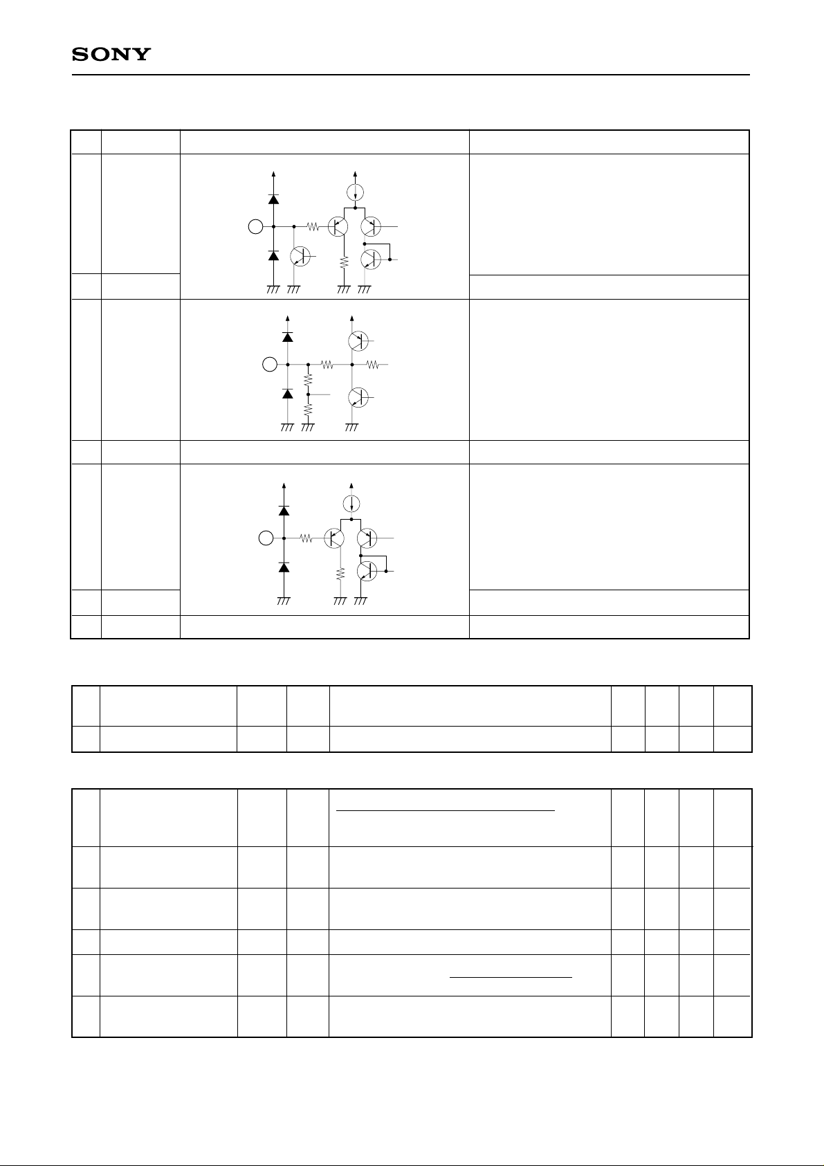
Equivalent circuit
CC
V
150
V
CC VCC
CC
V
150
VCC
4.5k
56
20k
20k
VCC
4.5k
Description
I/O pin for genera-purpose I/O port
VILmax: 1.5V
VIHmin:3V
VOLmax: 0.4V
SDA I/O pin for I2C bus
22k
D/A converter output pin
GND pin
Slave address input pin
Input at positive logic
VILmax: 1.5V
VIHmin:3V
15
16
SCL
VCC
SCL input pin for I2C bus
Power supply pin
Electrical Characteristics (Ta = 25°C, VCC = 9V)
No.
Circuit current
1
Item
Symbol
lcc
Test
circuit
1
Test conditions
DAC 0 to 4 = 127
Min.
8
Typ.
11
Max.
15
Unit
mA
D/A Converter Block
Differential linearity
2
Minimum output
3
voltage
Maximum output
4
voltage
Output current
5
Output impedance
6
DLE
Vmin
Vmax
Iout
Zo
V (DAC0 to 4 = n+1) – V (DAC0 to 4 = N)
1
V (DAC0 to 4 = 191) – V (DAC0 to 4 = 63)
n = 0 to 127
1
DAC 0 to 4 = 0
1
DAC 0 to 4 = 255
2
Current that can be flowed from Pins 3 to 7
2
DAC 0 to 4 = 127,
V (–1mA) – V (1mA)
2mA
×128–1
–1
0.1
8.3
–1
0
0
0.4
8.5
3
+1.1
0.62
8.9
+1
6
LSB
V
V
mA
Ω
Repple rejection
7
Grip
DAC 0 to 4 = 127, REF = 0
3
Superimose 100Hz to VCC, 1Vp-p
– 3 –
—
–60
–40
dB
SW, SAD Pins
CXA1315M/P
No.
Low level input
8
voItage
High level input
8
voltage
Low level input
9
current
High level input
10
current
Low level input
11
voltage
Item
Symbol
VIL
VIH
IIL
IIH
VOL
Test
circuit
4
4
4
4
5
Input voltage where ST0 to ST3 become "0"
Input voltage where ST0 to ST3 become "1"
lnput current when 0.4V is applied
lnput current when 4.5V is applied
SW 0 to 3 = 1,
Output voltage when 1mA flows in
I2C Bus Block Items (SDA, SCL)
No.
High level input voltage
13
Low level input voltage
14
High level input current
15
Low level input current
16
Low level output voltage, at 3mA flow to SDA (Pin 14)
17
Maximum flowing current
18
lnput capacitance
19
Maximum clock frequency
20
Data change minimum waiting time
21
Data transfer start minimum waiting time
22
Low level clock pulse width
23
High level clock pulse width
24
Minimum start preparation waiting time
25
Minimum data hold time
26
Minimum data preparation time
27
Rise time
28
Fall time
29
Minimum stop preparation waiting time
30
Item
Test conditions
Symbol
VIH
VIL
IIH
IIL
VOL
IOL
CI
fSCL
tBUF
tHD; STA
tLOW
tHIGH
tSU; STA
tHD; DAT
tSU; DAT
tR
tF
tSU; STO
Min.
—
3.0
–10
–10
0
Min.
3.0
0
—
—
0
3
—
0
4.7
4.0
4.7
4.0
4.7
5
250
—
—
4.7
Typ.
—
—
0
0
0.2
Typ.
—
—
—
—
—
—
—
—
—
—
—
—
—
—
—
—
—
—
Max.
1.5
—
+10
+10
0.4
Max.
5.0
1.5
10
10
0.4
—
10
100
—
—
—
—
—
—
—
1
300
—
Unit
V
V
µA
µA
V
Unit
V
V
µA
µA
V
mA
pF
kHz
µs
µs
µs
µs
µs
µs
ns
µs
ns
µs
I2C bus load conditions: Pull-up resistance 4kΩ (Connected to +5V)
Load capacitance 200pF (Connected to GND)
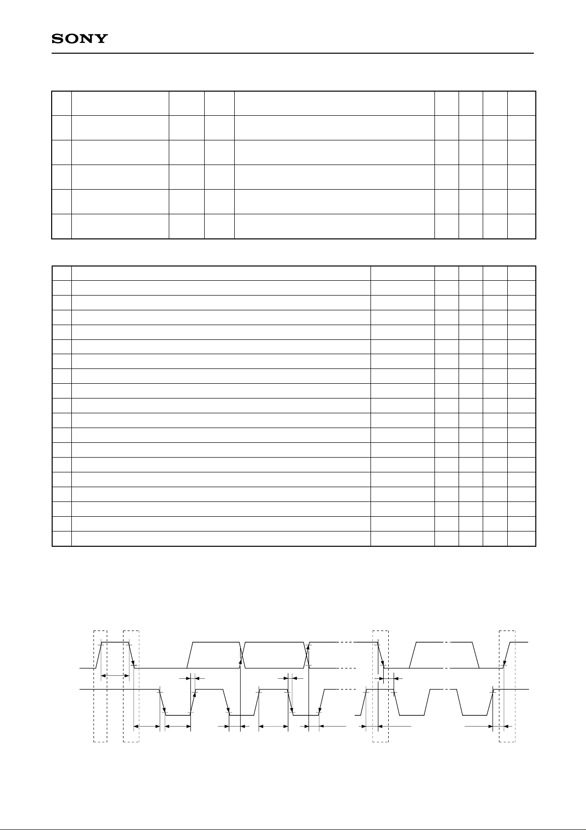
I2C Bus Control Signal
SDA
SCL
tBUF
PS Sr P
tHD; STA
tLOW
tR
tHD; DAT
tHIGH
tF
tSU; DAT
– 4 –
tHD; STA
tSU; STA
tSU; STO
 Loading...